SN74ALS153NSR,SN74AS153NSR,SN74ALS153DR,规格书,Datasheet 资料
双4选1数据选择器74LS153
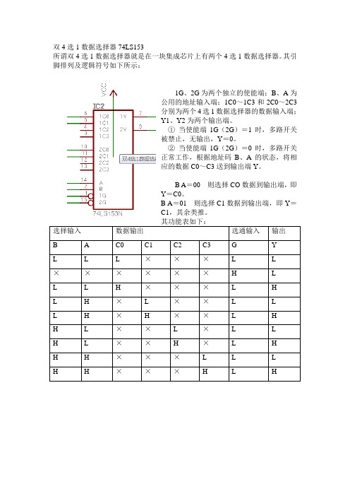
双4选1数据选择器74LS153
所谓双4选1数据选择器就是在一块集成芯片上有两个4选1数据选择器。
其引脚排列及逻辑符号如下所示:
1G、2G为两个独立的使能端;B、A为
公用的地址输入端;1C0~1C3和2C0~2C3
分别为两个4选1数据选择器的数据输入端;
Y1、Y2为两个输出端。
①当使能端1G(2G)=1时,多路开关
被禁止,无输出,Y=0。
②当使能端1G(2G)=0时,多路开关
正常工作,根据地址码B、A的状态,将相
应的数据C0~C3送到输出端Y。
B A=00 则选择CO数据到输出端,即
Y=C0。
B A=01 则选择C1数据到输出端,即Y=
C1,其余类推。
其功能表如下:
选择输入数据输出选通输入输出
B A C0 C1 C2 C3 G Y
L L L ×××L L
××××××H L
L L H ×××L H
L H ×L ××L L
L H ×H ××L H
H L ××L ×L L
H L ××H ×L H
H H ×××L L L
H H ×××H L H。
SN74AS00中文资料

元器件交易网IMPORTANT NOTICETexas Instruments and its subsidiaries (TI) reserve the right to make changes to their products or to discontinueany product or service without notice, and advise customers to obtain the latest version of relevant informationto verify, before placing orders, that information being relied on is current and complete. All products are soldsubject to the terms and conditions of sale supplied at the time of order acknowledgement, including thosepertaining to warranty, patent infringement, and limitation of liability.TI warrants performance of its semiconductor products to the specifications applicable at the time of sale inaccordance with TI’s standard warranty. Testing and other quality control techniques are utilized to the extentTI deems necessary to support this warranty. Specific testing of all parameters of each device is not necessarilyperformed, except those mandated by government requirements.CERTAIN APPLICATIONS USING SEMICONDUCTOR PRODUCTS MAY INVOLVE POTENTIAL RISKS OFDEATH, PERSONAL INJURY, OR SEVERE PROPERTY OR ENVIRONMENTAL DAMAGE (“CRITICALAPPLICATIONS”). TI SEMICONDUCTOR PRODUCTS ARE NOT DESIGNED, AUTHORIZED, ORWARRANTED TO BE SUITABLE FOR USE IN LIFE-SUPPORT DEVICES OR SYSTEMS OR OTHERCRITICAL APPLICATIONS. INCLUSION OF TI PRODUCTS IN SUCH APPLICATIONS IS UNDERSTOOD TOBE FULLY AT THE CUSTOMER’S RISK.In order to minimize risks associated with the customer’s applications, adequate design and operatingsafeguards must be provided by the customer to minimize inherent or procedural hazards.TI assumes no liability for applications assistance or customer product design. TI does not warrant or representthat any license, either express or implied, is granted under any patent right, copyright, mask work right, or otherintellectual property right of TI covering or relating to any combination, machine, or process in which suchsemiconductor products or services might be or are used. TI’s publication of information regarding any thirdparty’s products or services does not constitute TI’s approval, warranty or endorsement thereof.Copyright © 1998, Texas Instruments Incorporated。
74AC153

© 1999 Fairchild Semiconductor Corporation DS009928November 1988Revised November 199974AC153 • 74ACT153 Dual 4-Input Multiplexer74AC153 • 74ACT153Dual 4-Input MultiplexerGeneral DescriptionThe AC/ACT153 is a high-speed dual 4-input multiplexer with common select inputs and individual enable inputs for each section. It can select two lines of data from four sources. The two buffered outputs present data in the true (non-inverted) form. In addition to multiplexer operation,the AC/ACT153 can act as a function generator and gener-ate any two functions of three variables.Featuress I CC reduced by 50%s Outputs source/sink 24 mA s ACT153 has TTL-compatible inputsOrdering Code:Device also available in Tape and Reel. Specify by appending suffix letter “X” to the ordering code.Logic Symbols IEEE/IECConnection DiagramPin DescriptionsFACT is a trademark of Fairchild Semiconductor Corporation.Order Number Package NumberPackage Description74AC153SC M16A 16-Lead Small Outline Integrated Circuit (SOIC), JEDEC MS-012, 0.150” Narrow Body 74AC153SJ M16D 16-Lead Small Outline Package (SOP), EIAJ TYPE II, 5.3mm Wide74AC153MTC MTC1616-Lead Thin Shrink Small Outline Package (TSSOP), JEDEC MO-153, 4.4mm Wide 74AC153PC N16E 16-Lead Plastic Dual-In-Line Package (PDIP), JEDEC MS-001, 0.300” Wide74ACT153SC M16A 16-Lead Small Outline Integrated Circuit (SOIC), JEDEC MS-012, 0.150” Narrow Body 74ACT153MTCMTC1616-Lead Thin Shrink Small Outline Package (TSSOP), JEDEC MO-153, 4.4mm WidePin Names Description I 0a –I 3a Side A Data Inputs I 0b –I 3b Side B Data Inputs S 0, S 1 Common Select Inputs E a Side A Enable Input E b Side B Enable Input Z a Side A Output Z bSide B Output 274A C 153 • 74A C T 153Functional DescriptionThe AC/ACT153 is a dual 4-input multiplexer. It can select two bits of data from up to four sources under the control of the common Select inputs (S 0, S 1). The two 4-input multi-plexer circuits have individual active-LOW Enables (E a , E b )which can be used to strobe the outputs independently.When the Enables (E a , E b ) are HIGH, the corresponding outputs Z a , Z b ) are forced LOW. The AC/ACT153 is the logic implementation of a 2-pole, 4-position switch, where the position of the switch is determined by the logic levels supplied to the Select inputs. The logic equations for the outputs are shown below.Z a = E a • (I 0a • S 1 • S 0 + I 1a • S 1 • S 0 +I 2a • S 1 • S 0 + I 3a • S 1 • S 0)Z b = E b • (I 0b • S 1 • S 0 + I 1b • S 1 • S 0 +I 2b • S 1 • S 0 + I 3b • S 1 • S 0)Truth TableH = HIGH Voltage Level L = LOW Voltage Level X = ImmaterialLogic DiagramPlease note that this diagram is provided only for the understanding of logic operations and should not be used to estimate propagation delays.Select Inputs (a or b) Output Inputs S 0S 1E I 0I 1I 2I 3Z X X H X X X X L L L L L X X X L L L L H X X X H H L L XL X X L H L L X H X X H L H L X X L X L L H L X X H X H H H L X X X L L HHLXXXHH74AC153 • 74ACT153Absolute Maximum Ratings (Note 1)Recommended OperatingConditionsNote 1: Absolute maximum ratings are those values beyond which damage to the device may occur. The databook specifications should be met, with-out exception, to ensure that the system design is reliable over its power supply, temperature, and output/input loading variables. Fairchild does not recommend operation of FACT circuits outside databook specifications.DC Electrical Characteristics for ACNote 2: All outputs loaded; thresholds on input associated with output under test.Note 3: Maximum test duration 2.0 ms, one output loaded at a time.Note 4: I IN and I CC @ 3.0V are guaranteed to be less than or equal to the respective limit @ 5.5V V CC .Supply Voltage (V CC ) −0.5V to +7.0VDC Input Diode Current (I IK ) V I = −0.5V −20 mA V I = V CC + 0.5V +20 mADC Input Voltage (V I )−0.5V to V CC + 0.5VDC Output Diode Current (I OK ) V O = −0.5V −20 mA V O = V CC + 0.5V +20 mADC Output Voltage (V O ) −0.5V to V CC + 0.5VDC Output Source or Sink Current (I O ) ±50 mA DC V CC or Ground Current per Output Pin (I CC or I GND ) ±50 mAStorage Temperature (T STG ) −65°C to +150°CJunction Temperature (T J ) PDIP140°C Supply Voltage (V CC ) AC 2.0V to 6.0V ACT4.5V to5.5V Input Voltage (V I ) 0V to V CC Output Voltage (V O ) 0V to V CCOperating Temperature (T A ) −40°C to +85°CMinimum Input Edge Rate (∆V/∆t) AC Devices V IN from 30% to 70% of V CCV CC @ 3.3V, 4.5V, 5.5V125 mV/nsMinimum Input Edge Rate (∆V/∆t) ACT Devices V IN from 0.8V to 2.0VV CC @ 4.5V, 5.5V125 mV/nsSymbol ParameterV CC T A = +25°C T A = −40°C to +85°C UnitsConditions (V) Typ Guaranteed LimitsV IHMinimum HIGH Level 3.0 1.5 2.1 2.1V OUT = 0.1V Input Voltage4.5 2.25 3.15 3.15 V or V CC − 0.1V5.5 2.75 3.85 3.85V ILMaximum LOW Level 3.0 1.5 0.9 0.9V OUT = 0.1V Input Voltage4.5 2.25 1.35 1.35 Vor V CC − 0.1V 5.5 2.75 1.65 1.65V OHMinimum HIGH Level 3.0 2.99 2.9 2.9Output Voltage4.5 4.49 4.4 4.4 VI OUT = −50 µA 5.5 5.495.4 5.4V IN = V IL or V IH3.0 2.56 2.46I OH = −12 mA4.5 3.86 3.76 VI OH = −24 mA 5.54.86 4.76I OH = −24 mA (Note 2)V OLMaximum LOW Level 3.0 0.002 0.1 0.1Output Voltage4.5 0.001 0.1 0.1 VI OUT = 50 µA 5.5 0.0010.1 0.1V IN = V IL or V IH3.0 0.36 0.44I OL = 12 mA4.5 0.36 0.44 VI OL = 24 mA 5.50.36 0.44I OL = 24 mA (Note 2)I IN Maximum Input 5.5 ±0.1±1.0 µA V I = V CC , GND (Note 4)Leakage Current I OLD Minimum Dynamic 5.5 75 mA V OLD = 1.65V Max I OHD Output Current (Note 3) 5.5 −75 mA V OHD = 3.85V Min I CC Maximum Quiescent5.54.040.0µA V IN = V CC (Note 4)Supply Currentor GND 474A C 153 • 74A C T 153DC Electrical Characteristics for ACTNote 5: All outputs loaded; thresholds on input associated with output under test.Note 6: Maximum test duration 2.0 ms, one output loaded at a time.AC Electrical Characteristics for ACNote 7: Voltage Range 3.3 is 3.3V ± 0 3VVoltage Range 5.0 is 5.0V ± 0.5VSymbol ParameterV CC T A = +25°C T A = −40°C to +85°C Units Conditions (V) Typ Guaranteed LimitsV IH Minimum HIGH Level 4.5 1.5 2.0 2.0 VV OUT = 0.1V Input Voltage 5.5 1.5 2.0 2.0or V CC − 0.1VV IL Maximum LOW Level 4.5 1.50.80.8VV OUT = 0.1VInput Voltage 5.5 1.5 0.8 0.8or V CC − 0.1VV OHMinimum HIGH Level 4.5 4.49 4.4 4.4 VI OUT = −50 µAOutput Voltage5.5 5.495.4 5.4V IN = V IL or V IH4.5 3.86 3.76 VI OH = − 24 mA 5.54.86 4.76 I OH = − 24 mA (Note 5) V OLMaximum LOW Level 4.5 0.001 0.1 0.1V I OUT = 50 µA Output Voltage5.5 0.0010.1 0.1V IN = V IL or V IH4.5 0.36 0.44 VI OL = 24 mA 5.50.36 0.44 I OL = 24 mA (Note 5) I IN Maximum Input 5.5 ±0.1±1.0 µA V I = V CC , GNDLeakage Current I CCT Maximum 5.5 0.6 1.5 mA V I = V CC − 2.1V I CC /InputI OLD Minimum Dynamic 5.5 75 mA V OLD = 1.65V Max I OHD Output Current (Note 6) 5.5 −75 mAV OHD = 3.85V Min I CCMaximum Quiescent 5.54.040.0µA V IN = V CC Supply Currentor GNDV CCT A = +25°C T A = −40°C to +85°CSymbol Parameter(V)C L = 50 pFC L = 50 pF Units(Note 7) Min Typ Max Min Max t PLH Propagation Delay 3.3 2.5 9.5 15.0 2.5 17.5ns S n to Z n5.0 2.06.5 11.0 2.0 12.5 t PHL Propagation Delay 3.3 3.0 8.5 14.5 2.5 16.5ns S n to Z n5.0 2.56.5 11.0 2.0 12.0 t PLH Propagation Delay 3.3 2.5 8.0 13.5 2.0 16.0ns E to Z n5.0 1.5 5.5 9.51.5 11.0 t PHL Propagation Delay 3.32.5 7.0 11.0 2.0 12.5ns E to Z n5.0 2.0 5.0 8.01.5 9.0 t PLH Propagation Delay 3.32.5 7.5 12.5 2.0 14.5ns I n to Z n5.0 1.5 5.5 9.0 1.5 10.5 t PHLPropagation Delay 3.3 1.5 7.0 11.5 1.5 13.0nsI n to Z n5.01.55.08.51.510.074AC153 • 74ACT153AC Electrical Characteristics for ACTNote 8: Voltage Range 5.0 is 5.0V ± 0.5VCapacitanceV CCT A = +25°C T A = −40°C to +85°CSymbol Parameter(V)C L = 50 pFC L = 50 pF Units(Note 8) Min Typ Max Min Max t PLH Propagation Delay 5.0 3.0 7.0 11.5 2.013.5ns S n to Z nt PHL Propagation Delay 5.0 3.0 7.0 11.5 2.513.5ns S n to Z nt PLH Propagation Delay 5.02.06.510.52.012.5ns E n to Z nt PHL Propagation Delay 5.0 3.0 6.0 9.5 2.511.0ns E n to Z nt PLH Propagation Delay 5.0 2.5 5.5 9.5 2.011.0ns I n to Z nt PHLPropagation Delay 5.02.05.59.52.011.0nsI n to Z nSymbol ParameterTyp Units ConditionsC IN Input Capacitance4.5 pF V CC = OPEN C PDPower Dissipation Capacitance65.0pFV CC = 5.0V 674A C 153 • 74A C T 153Physical Dimensionsinches (millimeters) unless otherwise noted16-Lead Small Outline Integrated Circuit (SOIC), JEDEC MS-012, 0.150” Narrow BodyPackage Number M16A74AC153 • 74ACT153Physical Dimensionsinches (millimeters) unless otherwise noted (Continued)16-Lead Small Outline Package (SOP), EIAJ TYPE II, 5.3mm WidePackage Number M16D 874A C 153 • 74A C T 153Physical Dimensions inches (millimeters) unless otherwise noted (Continued)16-Lead Thin Shrink Small Outline Package (TSSOP), JEDEC MO-153, 4.4mm WidePackage Number MTC16974AC153 • 74ACT153 Dual 4-Input MultiplexerPhysical Dimensions inches (millimeters) unless otherwise noted (Continued)16-Lead Plastic Dual-In-Line Package (PDIP), JEDEC MS-001, 0.300” WidePackage Number N16EFairchild does not assume any responsibility for use of any circuitry described, no circuit patent licenses are implied and Fairchild reserves the right at any time without notice to change said circuitry and specifications.LIFE SUPPORT POLICYFAIRCHILD ’S PRODUCTS ARE NOT AUTHORIZED FOR USE AS CRITICAL COMPONENTS IN LIFE SUPPORT DEVICES OR SYSTEMS WITHOUT THE EXPRESS WRITTEN APPROVAL OF THE PRESIDENT OF FAIRCHILD SEMICONDUCTOR CORPORATION. As used herein:1.Life support devices or systems are devices or systems which, (a) are intended for surgical implant into the body, or (b) support or sustain life, and (c) whose failure to perform when properly used in accordance with instructions for use provided in the labeling, can be rea-sonably expected to result in a significant injury to the user.2. A critical component in any component of a life support device or system whose failure to perform can be rea-sonably expected to cause the failure of the life support device or system, or to affect its safety or effectiveness.。
SN7445N;SN7445NE4;SN7445NSR;SN7445NSRE4;SN7445NSRG4;中文规格书,Datasheet资料

PACKAG PACKAGING INFORMATIONOrderable Device Status (1)Package Type PackageDrawing Pins Package Qty Eco Plan (2)Lead/Ball FinishMSL PeaSN5445J ACTIVE CDIP J161TBD A42N / A for PkgSN7445N ACTIVE PDIP N1625Pb-Free (RoHS)CU NIPDAU N / A for PkgSN7445N ACTIVE PDIP N1625Pb-Free (RoHS)CU NIPDAU N / A for PkgSN7445N3OBSOLETE PDIP N16TBD Call TI Call TISN7445N3OBSOLETE PDIP N16TBD Call TI Call TISN7445NE4ACTIVE PDIP N1625Pb-Free (RoHS)CU NIPDAU N / A for PkgSN7445NE4ACTIVE PDIP N1625Pb-Free (RoHS)CU NIPDAU N / A for PkgSNJ5445J ACTIVE CDIP J161TBD A42N / A for PkgSNJ5445J ACTIVE CDIP J161TBD A42N / A for PkgSNJ5445W ACTIVE CFP W161TBD A42N / A for PkgSNJ5445W ACTIVE CFP W161TBD A42N / A for Pkg(1) The marketing status values are defined as follows:ACTIVE: Product device recommended for new designs.LIFEBUY: TI has announced that the device will be discontinued, and a lifetime-buy period is in effect.NRND: Not recommended for new designs. Device is in production to support existing customers, but TI does not recommend using this part in a new PREVIEW: Device has been announced but is not in production. Samples may or may not be available.OBSOLETE: TI has discontinued the production of the device.(2) Eco Plan - The planned eco-friendly classification: Pb-Free (RoHS), Pb-Free (RoHS Exempt), or Green (RoHS & no Sb/Br) - please check http://www.tinformation and additional product content details.TBD: The Pb-Free/Green conversion plan has not been defined.Pb-Free (RoHS): TI's terms "Lead-Free" or "Pb-Free" mean semiconductor products that are compatible with the current RoHS requirements for all lead not exceed 0.1% by weight in homogeneous materials. Where designed to be soldered at high temperatures, TI Pb-Free products are suitable fo Pb-Free (RoHS Exempt): This component has a RoHS exemption for either 1) lead-based flip-chip solder bumps used between the die and package, the die and leadframe. The component is otherwise considered Pb-Free (RoHS compatible) as defined above.Green (RoHS & no Sb/Br): TI defines "Green" to mean Pb-Free (RoHS compatible), and free of Bromine (Br) and Antimony (Sb) based flame retard in homogeneous material)(3) MSL, Peak Temp. -- The Moisture Sensitivity Level rating according to the JEDEC industry standard classifications, and peak solder temperature.Important Information and Disclaimer:The information provided on this page represents TI's knowledge and belief as of the date that it is provided. TI provided by third parties, and makes no representation or warranty as to the accuracy of such information. Efforts are underway to better integrate inf continues to take reasonable steps to provide representative and accurate information but may not have conducted destructive testing or chemical an TI and TI suppliers consider certain information to be proprietary, and thus CAS numbers and other limited information may not be available for releas //PACKAG Array In no event shall TI's liability arising out of such information exceed the total purchase price of the TI part(s) at issue in this document sold by TI to CuOTHER QUALIFIED VERSIONS OF SN5445, SN7445 :•Catalog: SN7445•Military: SN5445NOTE: Qualified Version Definitions:•Catalog - TI's standard catalog product•Military - QML certified for Military and Defense ApplicationsIMPORTANT NOTICETexas Instruments Incorporated and its subsidiaries(TI)reserve the right to make corrections,modifications,enhancements,improvements, and other changes to its products and services at any time and to discontinue any product or service without notice.Customers should obtain the latest relevant information before placing orders and should verify that such information is current and complete.All products are sold subject to TI’s terms and conditions of sale supplied at the time of order acknowledgment.TI warrants performance of its hardware products to the specifications applicable at the time of sale in accordance with TI’s standard warranty.Testing and other quality control techniques are used to the extent TI deems necessary to support this warranty.Except where mandated by government requirements,testing of all parameters of each product is not necessarily performed.TI assumes no liability for applications assistance or customer product design.Customers are responsible for their products and applications using TI components.To minimize the risks associated with customer products and applications,customers should provide adequate design and operating safeguards.TI does not warrant or represent that any license,either express or implied,is granted under any TI patent right,copyright,mask work right, or other TI intellectual property right relating to any combination,machine,or process in which TI products or services are rmation published by TI regarding third-party products or services does not constitute a license from TI to use such products or services or a warranty or endorsement e of such information may require a license from a third party under the patents or other intellectual property of the third party,or a license from TI under the patents or other intellectual property of TI.Reproduction of TI information in TI data books or data sheets is permissible only if reproduction is without alteration and is accompanied by all associated warranties,conditions,limitations,and notices.Reproduction of this information with alteration is an unfair and deceptive business practice.TI is not responsible or liable for such altered rmation of third parties may be subject to additional restrictions.Resale of TI products or services with statements different from or beyond the parameters stated by TI for that product or service voids all express and any implied warranties for the associated TI product or service and is an unfair and deceptive business practice.TI is not responsible or liable for any such statements.TI products are not authorized for use in safety-critical applications(such as life support)where a failure of the TI product would reasonably be expected to cause severe personal injury or death,unless officers of the parties have executed an agreement specifically governing such use.Buyers represent that they have all necessary expertise in the safety and regulatory ramifications of their applications,and acknowledge and agree that they are solely responsible for all legal,regulatory and safety-related requirements concerning their products and any use of TI products in such safety-critical applications,notwithstanding any applications-related information or support that may be provided by TI.Further,Buyers must fully indemnify TI and its representatives against any damages arising out of the use of TI products in such safety-critical applications.TI products are neither designed nor intended for use in military/aerospace applications or environments unless the TI products are specifically designated by TI as military-grade or"enhanced plastic."Only products designated by TI as military-grade meet military specifications.Buyers acknowledge and agree that any such use of TI products which TI has not designated as military-grade is solely at the Buyer's risk,and that they are solely responsible for compliance with all legal and regulatory requirements in connection with such use. TI products are neither designed nor intended for use in automotive applications or environments unless the specific TI products are designated by TI as compliant with ISO/TS16949requirements.Buyers acknowledge and agree that,if they use any non-designated products in automotive applications,TI will not be responsible for any failure to meet such requirements.Following are URLs where you can obtain information on other Texas Instruments products and application solutions:Products ApplicationsAudio /audio Communications and Telecom /communicationsAmplifiers Computers and Peripherals /computersData Converters Consumer Electronics /consumer-appsDLP®Products Energy and Lighting /energyDSP Industrial /industrialClocks and Timers /clocks Medical /medicalInterface Security /securityLogic Space,Avionics and Defense /space-avionics-defense Power Mgmt Transportation and Automotive /automotiveMicrocontrollers Video and Imaging /videoRFID OMAP Mobile Processors /omapWireless Connctivity /wirelessconnectivityTI E2E Community Home Page Mailing Address:Texas Instruments,Post Office Box655303,Dallas,Texas75265Copyright©2011,Texas Instruments Incorporated分销商库存信息:TISN7445N SN7445NE4SN7445NSR SN7445NSRE4SN7445NSRG4。
AS1530;AS1531;AS1530-T;AS1531-T;中文规格书,Datasheet资料

AS1530, AS153112-Bit, Single-Supply, Low-Power, 400/300ksps, 8-Channel A/D ConvertersD a ta S h e e t1 General DescriptionThe AS1530/AS1531 are low-power,8/4-channel, 400/300ksps, 12-bit analog-to-digital (A/D) converters specif-ically designed to operate with single-supply devices. Superior AC characteristics, very low power consump-tion, and highly-reliable packaging make these ultra-small devices perfect for battery-powered remote-sen-sor and data-acquisition devices.The successive-approximation register (SAR), high-speed sampling, high-bandwidth track/hold circuitry, and multi-mode operation combine to make these devices highly-flexible and configurable.Both devices require low supply current (2.8mA @400ksps, AS1530; 2.2mA @ 300ksps, AS1531) and fea-ture a reduced-power mode and a power-down mode to lower power consumption at slower throughput rates.The devices operate from a single supply (+4.5 to +5.5V, AS1530; +2.7 to +3.6V, AS1531). Both devices contain an internal 2.5V reference, an integrated referencebuffer, and feature support for an external reference (1V to V DD ).Data accesses are made via the high-speed, 4-wire, SPI, QSPI-, and Microwire-compatible serial interface.The devices are available in a 20-pin TSSOP package.Figure 1. Block Diagram and Pin Assignments2 Key Features! Single-Supply Operation:-+4.5 to +5.5V (AS1530)-+2.7 to +3.6V (AS1531)! Sampling Rate:-400ksps (AS1530)-300ksps (AS1531)! Software-Configurable Analog Input Types:-8-Channel Single-Ended-8-Channel Pseudo Differential Referenced to COM -4-Channel Pseudo Differential -4-Channel Fully Differential! Software-Configurable Input Range ! Internal +2.5V Reference ! Low-Current Operation:-2.8mA @ 400ksps (AS1530)-2.2mA @ 300ksps (AS1531)-0.4mA in Reduced-Power Mode -0.5µA in Full Power-Down Mode! SPI/QSPI/Microwire/TMS320-Compatible ! 20-pin TSSOP Package3 ApplicationsThe devices are ideal for remote sensors, data-acquisi-tion and data-logging devices, pen-digitizers, process control, or any other space-limited A/D application with low power-consumption requirements.AS1530/AS1531Control LogicOutput Shift Register12-Bit SARINOUT REFAnalog Input+1.2V REF Input Shift RegisterTrack/Hold 17k ΩAv ≈ 2.05+2.50V15SSTRB17CSN 14DOUT 20V DD119V DD213GND18SCLK16DIN1:8CH0:CH79COM12REFADJ11REF10V DD3AS1530/AS15311CH02CH13CH24CH35CH46CH57CH68CH79COM 10V DD320V DD119V DD218SCLK 17CSN16DIN 15SSTRB 14DOUT 13GND 12REFADJ 11REFData SheetContents1 General Description (1)2 Key Features (1)3 Applications (1)4 Pinout (3)Pin Assignments (3)Pin Descriptions (3)5 Absolute Maximum Ratings (4)6 Electrical Characteristics (5)AS1530 Electrical Characteristics (5)AS1531 Electrical Characteristics (7)Timing Characteristics (9)7 Typical Operating Characteristics (11)8 Detailed Description (14)Analog Input (14)Input Protection (14)Track/Hold (14)Control Register (15)Analog Input Configuration (15)Channel Selection (16)Single-Ended Input (16)Differential Input (16)Starting a Conversion (17)Transfer Functions (18)Power Modes (19)Reduced Power Mode (20)Full Power-Down Mode (20)Reference (21)Internal Reference (21)External Reference (22)9 Application Information (23)Initialization (23)Serial Interface (23)Serial Interface Configuration (23)QSPI Interface (24)Quick Evaluation Circuit (25)Layout Considerations (26)10 Package Drawings and Markings (27)11 Ordering Information (28)Data Sheet - Pi n o u t4 PinoutPin AssignmentsFigure 2. Pin Assignments (Top View)Pin DescriptionsTable 1. Pin Descriptions Pin NumberPin Name Description1:8CH0:CH7Analog Sampling Inputs. These eight pins serve as analog sampling inputs.9COM Common Analog Inputs . Tie this pin to ground in single-ended mode. 10V DD3Positive Supply Voltage11REFReference-Buffer Output/A/DC Reference Input . This pin serves as the reference voltage for analog-to-digital conversions. In internal reference mode, the reference buffer provides a +2.50V nominal output, externally adjustable at pin REFADJ. In external reference mode, disable the internal buffer by pulling pin REFADJ to V DD1.12REFADJ Reference-Buffer Amplifier Input . To disable the reference-buffer amplifier, tie this pin to V DD1.13GND Analog and Digital Ground14DOUT Serial Data Output . Data is clocked out at the rising edge of pin SCLK. DOUT is high impedance when CSN is high.15SSTRB Serial Strobe Output . SSTRB pulses high for one clock period before the MSB is clocked out. SSTRB is high impedance when CSN is high.16DIN Serial Data Input . Data is clocked in at the rising edge of SCLK.17CSN Active-Low Chip Select . Data will not be clocked into pin DIN unless CSN is low. When CSN is high, pins DOUT and SSTRB are high impedance.18SCLK Serial Clock Input . This pin clocks data into and out of the serial interface, and is used to set the conversion speed.Note:The duty cycle must be between 40 and 60%.19V DD2Positive Supply Voltage 20V DD1Positive Supply VoltageAS1530/AS15311CH02CH13CH24CH35CH46CH57CH68CH79COM 10V DD320V DD119V DD218SCLK 17CSN16DIN 15SSTRB 14DOUT 13GND 12REFADJ 11REFData Sheet- Ab s o l u te M a x i m u m R a t in g s5 Absolute Maximum RatingsStresses beyond those listed in Table 2 may cause permanent damage to the device. These are stress ratings only, and functional operation of the device at these or any other conditions beyond those indicated in Electrical Character-istics on page 5 is not implied. Exposure to absolute maximum rating conditions for extended periods may affect device reliability.Table 2. Absolute Maximum RatingsParameter Min Max Units Comments V DD1, V DD2, V DD3 to GND-0.3+7VV DD1 to V DD2 to V DD3-0.3+0.3VCH0:CH7, COM to GND-0.3V DD1 ++0.3VREF, REFADJ to GND-0.3V DD1 ++0.3VDIN, SCLK, CSN, to GND-0.3V DD2 ++0.3VDOUT, SSTRB to GND-0.3V DD2 ++0.3VDOUT, SSTRB Sink Current25mAContinuous Power Dissipation(T AMB = +70ºC)559mW Derate 7.0mW/ºC above +70ºC Operating Temperature Range-40+85ºCStorage Temperature Range-60+150ºCPackage Body Temperature+260ºC The reflow peak soldering temperature (body temperature) specified is in accordance with IPC/JEDEC J-STD-020C “Moisture/Reflow Sensitivity Classification for Non-Hermetic Solid State Surface Mount Devices”.The lead finish for Pb-free leaded packages ismatte tin (100% Sn).6 Electrical CharacteristicsAS1530 Electrical CharacteristicsV DD1 = V DD2 = V DD3 = +4.5 to +5.5V, COM = GND, f SCLK= 6.4MHz, 50% duty cycle, 16 clocks/conversion cycle(400ksps), external +2.5V at REF, REFADJ = V DD1, T AMB = T MIN to T MAX (unless otherwise specified). Typ values atT AMB = +25ºC.Table 3. AS1530 Electrical CharacteristicsSymbol Parameter Conditions Min Typ Max UnitsDC Accuracy1Resolution 12Bits INL Relative Accuracy 2-1+1LSBDNL Differential Nonlinearity No missing codes over temperature -1+1LSBOffset Error -6+6LSBGain Error 3-6+6LSBGain-Error TemperatureCoefficient ±1.6ppm/°CChannel-to-ChannelOffset Error Matching ±0.2LSB Dynamic Specifications: 100kHz sinewave input, 2.5Vp-p, 400ksps, 6.4MHz clock, bit RANGE(page 15) = 0, pseudo-differential input modeSINAD Signal-to-Noise plusDistortion Ratio 70 dB THD Total Harmonic Distortion Up to the 5th harmonic -82dBSFDRSpurious-FreeDynamic Range83dBIMD IntermodulationDistortion f IN1 = 99kHz, f IN2 = 102kHz 76 dB Channel-to-ChannelCrosstalk 4f IN = 200kHz, V IN = 2.5Vp-p -85dBFull-Power Bandwidth -3dB point 6 MHzFull-Linear Bandwidth SINAD > 68dB 450 kHz Conversion Ratet CONV Conversion Time 5 2.5 µs t ACQ Track/HoldAcquisitionTime 390ns t AD Aperture Delay 7ns t AJ Aperture Jitter <50 ps f SCLK SerialClockFrequency 0.5 6.4MHz Duty Cycle 40 60 % Analog Inputs: CH0:CH7, COMV CHx - V CHy (COM)Input Voltage Range: Single-Ended, Pseudo-Differential,and Differential 6Bit RANGE(page 15) = 10V REFVBit RANGE(page 15) = 0-V REF/2+V REF/2 Multiplexer Leakage Current On/off leakage current, V CHx = 0 or V DD1 -1±0.001+1 µA Input Capacitance 18 pFInternal ReferenceV REF REF Output Voltage T AMB = +25ºC 2.48 2.50 2.52 V REF Short-Circuit Current 30 mAT CVREF REF Output TemperatureCoefficient ±25ppm/°CLoad Regulation 70 to 1mA output load 1.2 4.0mV/ mAC BYPREF Capacitive Bypass at REF 4.7 10 µFC BYPREFADJ Capacitive Bypass at REFADJ0.01 10 µFREFADJ Output Voltage 1.22V REFADJ Input Range For small adjustments, from 1.22V ±100mV REFADJ Buffer DisableThresholdTo power down the internal reference1.4V DD1 -1V Buffer Voltage Gain2.045V/VExternal Reference : Reference buffer disabled, reference applied to pin REFREF Input Voltage Range81.0V DD1 + 50mVVREF Input CurrentV REF = 2.50V, f SCLK = 6.4MHz 200350 µAV REF = 2.50V, f SCLK = 0 320 Power-Down, f SCLK = 05Digital Inputs : DIN, SCLK, CSNV INH Input High Voltage 0.7 x V DDVV INL Input Low Voltage 0.3 xV DDVV HYST Input Hysteresis 0.2 VI IN Input Leakage V IN = 0 or V DD2 -1+1 µAC IN Input Capacitance 5 pFDigital Outputs : DOUT, SSTRB V OL Output Voltage Low I SINK = 5mA0.45VV OH Output Voltage High I SOURCE = 1mA 4 VI L Tri-State Leakage Current CSN = V DD2-10+10 µA C OUT Tri-State Output Capacitance CSN = V DD25pFPower Supply V DD1,V DD2, V DD3Positive Supply Voltage9 4.5 5.5 VI VDD1, I VDD2, I VDD3Supply CurrentV DD1 = V DD2 = V DD3 = 5.5VNormal Operation with External Reference 102.83.3mANormal Operation withInternal Reference 103.3 3.8Reduced-Power Mode 110.40.8Full Power-Down Mode0.52µA PSR Power-Supply RejectionV DD1 = V DD2 = V DD3 = 5V ±10%-2±0.1+2mV 1.Tested at V DD1 = V DD2 = V DD3 = +5V, COM = GND, bit RANGE (page 15) = 1, single-ended input mode.2.Relative accuracy is the deviation of the analog value at any code from its theoretical value after the gain error and offset error have been nulled.3.Offset nulled.4.Ground on channel; sinewave applied to all off channels.5.Conversion time is defined as the number of clock cycles multiplied by the clock period; clock has 50% duty cycle.6.The absolute voltage range for the analog inputs (CH0:CH7, and COM) is from GND to V DD1.7.External load should not change during conversion for specified accuracy. Guaranteed specification of 4mV/mA is a result of production test limitations.8.AS1530/AS1531 performance is limited by the device noise floor, typically 300µVp-p.Table 3. AS1530 Electrical Characteristics (Continued)Symbol Parameter Conditions Min Typ Max UnitsAS1531 Electrical CharacteristicsV DD1 = V DD2 = V DD3 = +2.7 to +3.6V, COM = GND, f SCLK = 4.8MHz, 50% duty cycle, 16 clocks/conversion cycle (300ksps), external +2.5V at REF, REFADJ = V DD1, T AMB = T MIN to T MAX (unless otherwise specified). Typ values at T AMB = +25ºC.9.Electrical characteristics are guaranteed from V DD1(MIN) = V DD2(MIN) = V DD3(MIN) to V DD1(MAX) = V DD2(MAX) = V DD3(MAX). For operations beyond this range, see Typical Operating Characteristics on page 11. For guaranteed specifications beyond the limits, contact austriamicrosystems, AG.10. AIN = mid-scale; bit RANGE (page 15) = 1; tested with 20pF on DOUT, 20pF on SSTRB, and f SCLK = 6.4MHz @ GND to V DD2.11. SCLK = DIN = GND, CSN = V DD2.Table 4. AS1531 Electrical Characteristics Symbol Parameter Conditions Min Typ Max UnitsDC Accuracy 1Resolution 12 Bits INL Relative Accuracy 2-1+1LSB DNLDifferential NonlinearityNo missing codes over temperature-1+1LSB Offset Error-6+6LSBGain Error3-6+6LSB Gain-Error Temperature Coefficient ±1.6ppm/°CChannel-to-Channel OffsetError Matching±0.2 LSBDynamic Specifications : 75kHz sinewave input, 2.5Vp-p, 300ksps, 4.8MHz clock, bit RANGE (page 15) = 0, pseudo-differential input modeSINAD Signal-to-Noise plusDistortion Ratio70 dBTHD Total Harmonic Distortion Up to the 5th harmonic -81 dBSFDR Spurious-Free DynamicRange84 dBIMD Intermodulation Distortion f IN1 = 73kHz, f IN2 = 77kHz76 dB Channel-to-ChannelCrosstalk4f IN = 150kHz, V IN = 2.5Vp-p -80dB Full-Power Bandwidth -3dB point 6MHz Full-Linear Bandwidth SINAD > 68dB 350 kHzConversion Ratet CONVConversion Time5Normal operation 3.3µs t ACQ Track/Hold Acquisition Time Normal operation520ns t AD Aperture Delay 7ns t AJ Aperture Jitter<50ps f SCLKSerial Clock Frequency Normal operation0.5 4.8 MHz Duty Cycle40 60%Analog Inputs: CH0:CH7, COMV CHx - V CHy(COM)Input Voltage Range: Single-Ended, Pseudo-Differential, and Differential 6Bit RANGE (page 15) = 10V REFV Bit RANGE (page 15) = 0-V REF/2+V REF /2 Multiplexer Leakage CurrentOn/off leakage current, V CHx = 0 or A VDD-1±0.001+1 µAInput Capacitance18 pF Internal ReferenceV REFREF Output Voltage T AMB = +25°C2.482.50 2.52V REF Short-Circuit Current30mAT CVREFREF OutputTemperature Coefficient ±25ppm/°C Load Regulation70 to 0.75mA output load0.6 2.0 mV/mA C BYPREFCapacitive Bypass at REF4.710µFC BYPREFADJ Capacitive Bypass at REFADJ0.01 10 µFREFADJ Output Voltage 1.22V REFADJ Input Range For small adjustments, from 1.22V ±100mV REFADJ BufferDisable Threshold To power down the internal reference1.4V DD1 - 1V Buffer Voltage Gain2.045V/V External Reference : Reference buffer disabled, reference applied to REFREF Input Voltage Range81.0V DD1 + 50mV V REF Input CurrentV REF = 2.50V, f SCLK = 4.8MHz 200350 µAV REF = 2.50V, f SCLK = 0 320 In power-down, f SCLK = 05 Digital Inputs : DIN, SCLK, CSN V INH Input High Voltage 0.7 x V DDVV INL Input Low Voltage 0.3 x V DDVV HYST Input Hysteresis 0.8VI IN Input Leakage V IN = 0 or V DD2 -1+1 µA C IN InputCapacitance 5pF Digital Outputs : DOUT, SSTRBV OL Output Voltage Low I SINK = 5mA 0.45V V OH Output Voltage HighI SOURCE = 0.5mA V DD2 - 0.5V VI LTri-State Leakage CurrentCSN = V DD2-10+10 µAC OUT Tri-State OutputCapacitance CSN = V DD25pFPower Supply V DD1,V DD2, V DD3Positive Supply Voltage9 2.7 3.6 VI VDD1, I VDD2, I VDD3Supply CurrentV DD1 = V DD2 = V DD3 = 5.5VNormal Operationwith ExternalReference102.2 2.7Normal Operation with InternalReference 102.73.2mAReduced-PowerMode110.40.8Full Power-DownMode110.5 2 µAPSR Power-Supply RejectionV DD1 = V DD2 = V DD3= 2.7 to 3.6V, Mid-Scale Input-2±0.1+2 mV1.Tested at V DD1 = V DD2 = V DD3 = +3V; COM = GND; bit RANGE (page 15) = 1, single-ended input mode.Table 4. AS1531 Electrical Characteristics (Continued)Symbol Parameter Conditions Min Typ MaxUnitsTiming Characteristics2.Relative accuracy is the deviation of the analog value at any code from its theoretical value after the gain error and offset error have been nulled.3.Offset nulled.4.Ground on channel; sinewave applied to all off channels.5.Conversion time is defined as the number of clock cycles multiplied by the clock period; clock has 50% duty cycle.6.The absolute voltage range for the analog inputs (CH0:CH7, and COM) is from GND to V DD1.7.External load should not change during conversion for specified accuracy. Guaranteed specification of 2mV/mA is a result of production test limitations.8.AS1530/AS1531 performance is limited by the device noise floor, typically 300µVp-p.9.Electrical characteristics are guaranteed from V DD1(MIN) = V DD2(MIN) = V DD3(MIN) to V DD1(MAX) = V DD2(MAX) = V DD3(MAX). For operations beyond this range, see Typical Operating Characteristics on page 11. For guaranteed specifications beyond the limits, contact austriamicrosystems, AG.10. AIN = mid-scale; bit RANGE (page 15) = 1; tested with 20pF on DOUT, 20pF on SSTRB, and f SCLK = 4.8MHz @ GND to V DD2.11. SCLK = DIN = GND, CSN = V DD2.Table 5. AS1530 Timing Characteristics – (Figures 3, 4, 21, 23; V DD1 = V DD2 = V DD3 = +4.5 to +5.5V; T AMB = T MIN to T MAX (unless otherwise specified). Symbol Parameter ConditionsMin TypMaxUnitst CP SCLK Period156ns t CH SCLK Pulse Width High 62 ns t CL SCLK Pulse Width Low 62 ns t DS DIN to SCLK Setup 35 ns t DH DIN to SCLK Hold 0 ns t CSS CSN Fall to SCLK Rise Setup 35 ns t CS0 SCLK Rise to CSN Fall Ignore 35 ns t DOH SCLK Rise to DOUT Hold C LOAD = 20pF 10 20ns t STH SCLK Rise to SSTRB Hold C LOAD = 20pF 1020ns t STV SCLK Rise to DOUT Valid C LOAD = 20pF 80 ns t DOV SCLK Rise to SSTRB Valid C LOAD = 20pF 80 ns t DOD CSN Rise to DOUT Disable C LOAD = 20pF 10 65 ns t STD CSN Rise to SSTRB Disable C LOAD = 20pF 1065 ns t DOE CSN Fall to DOUT Enable C LOAD = 20pF 65 ns t STE CSN Fall to SSTRB Enable C LOAD = 20pF65ns t CSWCSN Pulse Width High100 nsTable 6. AS1531 Timing Characteristics – (Figures 3, 4, 21, 23; V DD1 = V DD2 = V DD3 = +2.7 to +3.6V; T AMB = T MIN to T MAX (unless otherwise specified).Symbol Parameter ConditionsMin TypMaxUnitst CP SCLK Period208ns t CH SCLK Pulse Width High 83 ns t CL SCLK Pulse Width Low 83 ns t DS DIN to SCLK Setup 45 ns t DH DIN to SCLK Hold 0 ns t CSS CSN Fall to SCLK Rise Setup 45 ns t CS0 SCLK Rise to CSN Fall ignore 45 ns t DOH SCLK Rise to DOUT Hold C LOAD = 20pF 13 20ns t STHSCLK Rise to SSTRB HoldC LOAD = 20pF 1320nsFigure 3. DOUT Enable-Time Load CircuitsFigure 4. DOUT Disable-Time Load Circuitst DOV SCLK Rise to DOUT Valid C LOAD = 20pF 100 ns t STV SCLK Rise to SSTRB Valid C LOAD = 20pF 100ns t DOD CSN Rise to DOUT Disable C LOAD = 20pF 13 85ns t STD CSN Rise to SSTRB Disable C LOAD = 20pF 13 85ns t DOE CSN Fall to DOUT Enable C LOAD = 20pF 85ns t STE CSN Fall to SSTRB Enable C LOAD = 20pF85ns t CSWCSN Pulse Width High100 nsTable 6. AS1531 Timing Characteristics – (Figures 3, 4, 21, 23; V DD1 = V DD2 = V DD3 = +2.7 to +3.6V; T AMB = T MIN to T MAX (unless otherwise specified). (Continued)Symbol ParameterConditions MinTypMax Units C LOAD 20pFC LOAD 20pF6k ΩGNDDGNDDOUTDOUTHigh-impedance to V OH and V OL to V OHV DD2High-impedance to V OL and V OH to V OL6k ΩDGND 6k ΩC LOAD 20pFC LOAD 20pF6k ΩDGNDGNDDGNDDOUTDOUTV OH to high-impedanceV DD2V OL to high-impedance分销商库存信息:AMSAS1530AS1531AS1530-T AS1531-T。
,CD74HC153M96,CD74HC153M96E4,CD74HC153M96G4,CD74HCT153EE4,CD74HC153E, 规格书,Datasheet 资料

ENABLE OUTPUT
E
Y
H
L
L
L
L
H
L
L
L
H
L
L
L
H
L
L
L
H
2 芯天下--/
CD54HC153, CD74HC153, CD54HCT153, CD74HCT153
Absolute Maximum Ratings
DC Supply Voltage, VCC . . . . . . . . . . . . . . . . . . . . . . . . -0.5V to 7V DC Input Diode Current, IIK
CAUTION: Stresses above those listed in “Absolute Maximum Ratings” may cause permanent damage to the device. This is a stress only rating and operation of the device at these or any other conditions above those indicated in the operational sections of this specification is not implied.
-5.2
6
VOL VIH or VIL 0.02
L
X
X
L
H
X
H
X
X
H
L
X
X
L
X
H
L
X
X
H
X
H
H
X
X
X
L
H
DM74LS153N中文资料

© 2000 Fairchild Semiconductor Corporation DS006393August 1986Revised March 2000DM74LS153 Dual 1-of-4 Line Data Selectors/MultiplexersDM74LS153Dual 1-of-4 Line Data Selectors/MultiplexersGeneral DescriptionEach of these data selectors/multiplexers contains invert-ers and drivers to supply fully complementary, on-chip,binary decoding data selection to the AND-OR-invert gates. Separate strobe inputs are provided for each of the two four-line sections.Featuress Permits multiplexing from N lines to 1 line s Performs at parallel-to-serial conversion s Strobe (enable) line provided for cascading (N lines to n lines)s High fan-out, low impedance, totem pole outputs s Typical average propagation delay times From data 14 ns From strobe 19 ns From select22 nss Typical power dissipation 31 mWOrdering Code:Devices also available in T ape and Reel. Specify by appending the suffix letter “X” to the ordering code.Connection Diagram Function TableSelect inputs A and B are common to both sections.H = HIGH Level L = LOW Level X = Don't CareOrder Number Package NumberPackage DescriptionDM74LS153M M16A 16-Lead Small Outline Integrated Circuit (SOIC), JEDEC MS-012, 0.150 Narrow DM74LS153NN16E16-Lead Plastic Dual-In-Line Package (PDIP), JEDEC MS-001, 0.300 WideSelect Data Inputs Strobe Output Inputs B A C0C1C2C3G Y X X X X X X H L L L L X X X L L L L H X X X L H L H X L X X L L L H X H X X L H H L X X L X L L H L X X H X L H H H X X X L L L HHXXXHLH 2D M 74L S 153Logic DiagramDM74LS153Absolute Maximum Ratings (Note 1)Note 1: The “Absolute Maximum Ratings” are those values beyond which the safety of the device cannot be guaranteed. The device should not be operated at these limits. The parametric values defined in the Electrical Characteristics tables are not guaranteed at the absolute maximum ratings.The “Recommended Operating Conditions” table will define the conditions for actual device operation.Recommended Operating ConditionsElectrical Characteristicsover recommended operating free air temperature range (unless otherwise noted)Note 2: All typicals are at V CC = 5V, T A = 25° C.Note 3: Not more than one output should be shorted at a time, and the duration should not exceed one second.Note 4: I CC is measured with all outputs OPEN and all other inputs GROUNDED.Switching Characteristicsat V CC = 5V and T A = 25°CSupply Voltage 7V Input Voltage7VOperating Free Air Temperature Range 0°C to +70°C Storage Temperature Range−65°C to +150° CSymbol ParameterMin Nom Max Units V CC Supply Voltage4.7555.25V V IH HIGH Level Input Voltage 2V V IL LOW Level Input Voltage 0.8V I OH HIGH Level Output Current −0.4mA I OL LOW Level Output Current 8mA T AFree Air Operating Temperature70°CSymbol ParameterConditionsMinTyp Max Units (Note 2)V I Input Clamp Voltage V CC = Min, I I = −18 mA −1.5V V OH HIGH Level V CC = Min, I OH = Max 2.73.4VOutput Voltage V IL = Max, V IH = Min V OLLOW Level V CC = Min, I OL = Max0.350.5Output VoltageV IL = Max, V IH = Min VI OL = 4 mA, V CC = Min 0.250.4I I Input Current @ Max Input Voltage V CC = Max, V I = 7V 0.1mA I IH HIGH Level Input Current V CC = Max, V I = 2.7V 20µA I IL LOW Level Input Current V CC = Max, V I = 0.4V −0.36mA I OS Short Circuit Output Current V CC = Max (Note 3)−20−100mA I CCSupply CurrentV CC = Max (Note 4)6.210mAFrom (Input)R L = 2 k ΩSymbol Parameterto (Output)C L = 15 pF C L = 50 pF UnitsMinMax MinMax t PLH Propagation Delay Time Data to Y 1520ns LOW-to-HIGH Level Output t PHL Propagation Delay Time Data to Y 2635ns HIGH-to-LOW Level Output t PLH Propagation Delay Time Select to Y 2935ns LOW-to-HIGH Level Output t PHL Propagation Delay Time Select to Y 3845ns HIGH-to-LOW Level Output t PLH Propagation Delay Time Strobe to Y 2430ns LOW-to-HIGH Level Output t PHLPropagation Delay Time Strobe to Y3240ns HIGH-to-LOW Level Output 4D M 74L S 153Physical Dimensionsinches (millimeters) unless otherwise noted16-Lead Small Outline Integrated Circuit (SOIC), JEDEC MS-012, 0.150 NarrowPackage Number M16A5DM74LS153 Dual 1-of-4 Line Data Selectors/MultiplexersPhysical Dimensions inches (millimeters) unless otherwise noted (Continued)16-Lead Plastic Dual-In-Line Package (PDIP), JEDEC MS-001, 0.300 WidePackage Number N16EFairchild does not assume any responsibility for use of any circuitry described, no circuit patent licenses are implied and Fairchild reserves the right at any time without notice to change said circuitry and specifications.LIFE SUPPORT POLICYFAIRCHILD’S PRODUCTS ARE NOT AUTHORIZED FOR USE AS CRITICAL COMPONENTS IN LIFE SUPPORT DEVICES OR SYSTEMS WITHOUT THE EXPRESS WRITTEN APPROVAL OF THE PRESIDENT OF FAIRCHILD SEMICONDUCTOR CORPORATION. As used herein:1.Life support devices or systems are devices or systems which, (a) are intended for surgical implant into the body, or (b) support or sustain life, and (c) whose failure to perform when properly used in accordance with instructions for use provided in the labeling, can be rea-sonably expected to result in a significant injury to the user.2. A critical component in any component of a life support device or system whose failure to perform can be rea-sonably expected to cause the failure of the life support device or system, or to affect its safety or effectiveness.。
74LV153PW中文资料
元器件交易网DIP16:plastic dual in-line package; 16 leads (300 mil)SOT38-4SO16:plastic small outline package; 16 leads; body width 3.9 mm SOT109-1SSOP16:plastic shrink small outline package; 16 leads; body width 5.3 mm SOT338-1TSSOP16:plastic thin shrink small outline package; 16 leads; body width 4.4 mm SOT403-1NOTESNOTESPhilips Semiconductors and Philips Electronics North America Corporation reserve the right to make changes, without notice, in the products,including circuits, standard cells, and/or software, described or contained herein in order to improve design and/or performance. Philips Semiconductors assumes no responsibility or liability for the use of any of these products, conveys no license or title under any patent, copyright,or mask work right to these products, and makes no representations or warranties that these products are free from patent, copyright, or mask work right infringement, unless otherwise specified. Applications that are described herein for any of these products are for illustrative purposes only. Philips Semiconductors makes no representation or warranty that such applications will be suitable for the specified use without further testing or modification.LIFE SUPPORT APPLICATIONS Philips Semiconductors and Philips Electronics North America Corporation Products are not designed for use in life support appliances, devices,or systems where malfunction of a Philips Semiconductors and Philips Electronics North America Corporation Product can reasonably be expected to result in a personal injury. Philips Semiconductors and Philips Electronics North America Corporation customers using or selling Philips Semiconductors and Philips Electronics North America Corporation Products for use in such applications do so at their own risk and agree to fully indemnify Philips Semiconductors and Philips Electronics North America Corporation for any damages resulting from such improper use or sale.This data sheet contains preliminary data, and supplementary data will be published at a later date. PhilipsSemiconductors reserves the right to make changes at any time without notice in order to improve designand supply the best possible product.Philips Semiconductors811 East Arques AvenueP .O. Box 3409Sunnyvale, California 94088–3409Telephone 800-234-7381DEFINITIONSData Sheet IdentificationProduct Status Definition Objective Specification Preliminary Specification Product Specification Formative or in Design Preproduction Product Full ProductionThis data sheet contains the design target or goal specifications for product development. Specificationsmay change in any manner without notice.This data sheet contains Final Specifications. Philips Semiconductors reserves the right to make changesat any time without notice, in order to improve design and supply the best possible product.© Copyright Philips Electronics North America Corporation 1998All rights reserved. Printed in U.S.A.print codeDate of release: 05-96。
- 1、下载文档前请自行甄别文档内容的完整性,平台不提供额外的编辑、内容补充、找答案等附加服务。
- 2、"仅部分预览"的文档,不可在线预览部分如存在完整性等问题,可反馈申请退款(可完整预览的文档不适用该条件!)。
- 3、如文档侵犯您的权益,请联系客服反馈,我们会尽快为您处理(人工客服工作时间:9:00-18:30)。
SN54ALS153, SN74ALS153, SN74AS153DUAL 1ĆOFĆ4 DATA SELECTORS/MULTIPLEXERSą SDAS206A − APRIL 1982 − REVISED DECEMBER 1994
Copyright 1994, Texas Instruments Incorporated1POST OFFICE BOX 655303 • DALLAS, TEXAS 75265
POST OFFICE BOX 1443 • HOUSTON, TEXAS 77251−1443
•Permit Multiplexing From n Lines to
One Line•Perform Parallel-to-Serial Conversion
•Strobe (Enable) Line Provided for
Cascading (n Lines to n Lines)•′ALS253 and SN74AS253A Are 3-State
Versions of These Parts•Package Options Include Plastic
Small-Outline (D) Packages, Ceramic ChipCarriers (FK), and Standard Plastic (N) andCeramic (J) 300-mil DIPs
descriptionThese dual 1-of-4 data selectors/multiplexerscontain inverters and drivers to supply full binarydecoding data selection to the AND-OR gates.Separate strobe (G) inputs are provided for eachof the two 4-line sections.
The SN54ALS153 is characterized for operationover the full military temperature range of −55°Cto 125°C. The SN74ALS153 and SN74AS153 arecharacterized for operation from 0°C to 70°C.
FUNCTION TABLEINPUTSSTROBEOUTPUTSELECTDATAGY
BAC0C1C2C3
XXXXXXHLLLLXXXLLLLHXXXLHLHXLXXLLLHXHXXLHHLXXLXLLHLXXHXLHHHXXXLLLHHXXXHLHSelect inputs A and B are common to both sections.
SN54ALS153...J PACKAGESN74ALS153, SN74AS153...D OR N PACKAGE(TOP VIEW)
32120199101112134
5678
1817161514
A2C3NC2C22C1
1C31C2NC1C11C0
SN54ALS153...FK PACKAGE(TOP VIEW)
B1
GNC
2Y2C0
2G1YGND
NC
NC − No internal connection
VCC
12345678
161514131211109
1GB1C31C21C11C01YGNDVCC2GA2C32C22C12C02Y
PRODUCTION DATA information is current as of publication date.Products conform to specifications per the terms of Texas Instrumentsstandard warranty. Production processing does not necessarily includetesting of all parameters.
芯天下--http://oneic.com/SN54ALS153, SN74ALS153, SN74AS153DUAL 1ĆOFĆ4 DATA SELECTORS/MULTIPLEXERSąSDAS206A − APRIL 1982 − REVISED DECEMBER 1994
2POST OFFICE BOX 655303 • DALLAS, TEXAS 75265
POST OFFICE BOX 1443 • HOUSTON, TEXAS 77251−1443
logic symbol†GMUX0
3
014A
12B
EN1
151Y7061C0151C1241C2331C3
102C0112C1122C2132C3
2Y9
1G2G†This symbol is in accordance with ANSI/IEEE Std 91-1984 and IEC Publication 617-12.
Pin numbers shown are for the D, J, and N packages.
logic diagram (positive logic)
Data 2SelectData 1
2G2C32C22C12C0AB1C31C2
1C1
1C01G1Y1
65432
1410
11121315
72Y9Pin numbers shown are for the D, J, and N packages.芯天下--http://oneic.com/SN54ALS153, SN74ALS153, SN74AS153DUAL 1ĆOFĆ4 DATA SELECTORS/MULTIPLEXERSą SDAS206A − APRIL 1982 − REVISED DECEMBER 1994
3POST OFFICE BOX 655303 • DALLAS, TEXAS 75265
POST OFFICE BOX 1443 • HOUSTON, TEXAS 77251−1443
absolute maximum ratings over operating free-air temperature range (unless otherwise noted)†Supply voltage, VCC 7 V. . . . . . . . . . . . . . . . . . . . . . . . . . . . . . . . . . . . . . . . . . . . . . . . . . . . . . . . . . . . . . . . . . . . . . . . Input voltage, VI 7 V. . . . . . . . . . . . . . . . . . . . . . . . . . . . . . . . . . . . . . . . . . . . . . . . . . . . . . . . . . . . . . . . . . . . . . . . . . . .
Operating free-air temperature range, TA:SN54ALS153 −55°C to 125°C. . . . . . . . . . . . . . . . . . . . . . . . . . . . . . SN74ALS153 0°C to 70°C. . . . . . . . . . . . . . . . . . . . . . . . . . . . . . . . . Storage temperature range −65°C to 150°C. . . . . . . . . . . . . . . . . . . . . . . . . . . . . . . . . . . . . . . . . . . . . . . . . . . . . . . .
†Stresses beyond those listed under “absolute maximum ratings” may cause permanent damage to the device. These are stress ratings only, and
functional operation of the device at these or any other conditions beyond those indicated under “recommended operating conditions” is notimplied. Exposure to absolute-maximum-rated conditions for extended periods may affect device reliability.
recommended operating conditionsSN54ALS153SN74ALS153MINNOMMAXMINNOMMAXUNIT
VCCSupply voltage4.555.54.555.5VVIHHigh-level input voltage22VVILLow-level input voltage0.70.8VIOHHigh-level output current−1−2.6mAIOLLow-level output current1224mATAOperating free-air temperature−55125070°C
electrical characteristics over recommended operating free-air temperature range (unlessotherwise noted)
SN54ALS153SN74ALS153PARAMETERTEST CONDITIONSMINTYP‡MAXMINTYP‡MAXUNIT
VIKVCC = 4.5 V,II = −18 mA−1.5−1.5VVCC = 4.5 V to 5.5 V,IOH = −0.4 mAVCC −2VCC −2VVIOH = −1 mA2.43.3OHCC = 4.5 VIOH = −2.6 mA2.43.2V
IOL = 12 mA0.250.40.250.4VOLVCC = 4.5 VIOL = 24 mA0.350.5V
IIVCC = 5.5 V,VI = 7 V0.10.1mAIIHVCC = 5.5 V,VI = 2.7 V2020µAIILVCC = 5.5 V,VI = 0.4 V−0.1−0.1mAIO§VCC = 5.5 V,VO = 2.25 V−20−112−30−112mAICCVCC = 5.5 V,All inputs at 4.5 V7.5147.514mA‡All typical values are at VCC = 5 V, TA = 25°C.