RX-8025T规格书(中文)
8025t中文使用详细说明
RX-8025T 使用说明概要
1、8025T 的特点:
1. 内置高稳定度的 32.768KHz 的 DTCXO (数字温度补偿晶体振荡器) 2. 支持 I2C 总线的高速模式(400K)。 3. 定时报警功能(可设定:天,日期,小时,分钟) 4. 固定周期定时中断功能。 5. 时间更新中断功能。 6. 32.768KHz 频率输出(具有使能 OE 功能) 7. 闰年自动调整功能。(2000 到 2099) 8. 宽范围接口电压:2.2V 到 5.5V 9. 宽范围的时间保持电压:1.8V 到 5.5V 10. 低电流功耗:0.8uA/3V (Typ.)
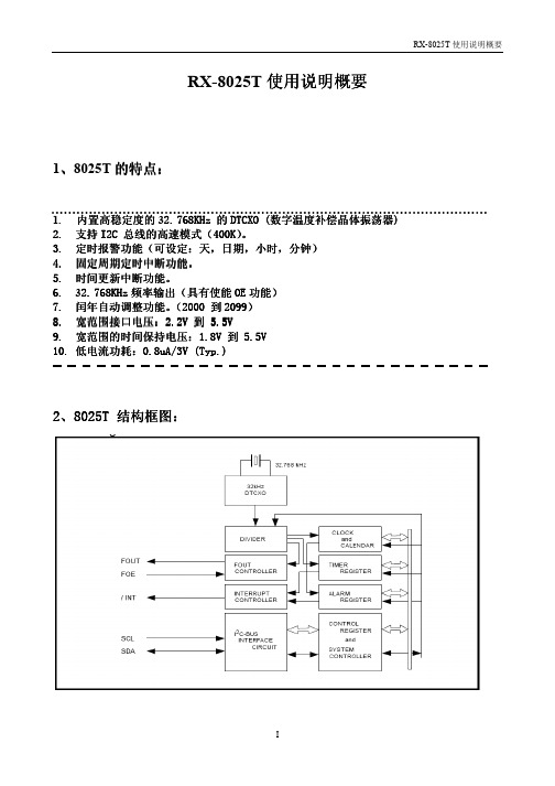
2、8025T 结构框图:
I
3、 8025T 管脚定义:
RX-8025T 使用说明概要
3.1 管脚功能定义:
管脚名称
I/O
功能
1:T1
In
* 工厂测试用(不用额外连接)
2:SCL
In
I2C 总线通讯的串行时钟输入端
3:FOUT
Out
这是个 C-MOS 输出引脚,可通过 FOE 进行控制。
当 FOE=’H’,该引脚输出一个 32.768KHz 信号
时钟计数器(寄存器 0 到 2)
分别记录时钟的-时,分,秒 所有的数据格式都为 BCD 码,例如秒寄存器的值为 ‘0101 1001’ 实际表示为 59 秒。 小时计数器从‘00’‘01’一直到‘23’,然后重新从‘00’开始,为 24 小时进制。
星期寄存器 REG-3
该寄存器用来记录星期的信息:第 0 位到第 6 位用来表示星期日,星期一....到星期六。 数据格式不再是 BCD 编码,而是分别用一位来表示不同的日期。
RX-8025T使用说明概要

条件
接口电压 温度补偿电压 -
Min.
1.8 2.2 1.6 -40
Typ.
3.0 3.0 3.0 +25
6、频率特性:
频率稳定度: ▵f/f= ±3.8ppm @ Ta= 0 to +50℃, VDD=3.0V 相当于:60*60*24*3.8ppm = 0.328 (85℃, VDD=3.0V 相当于:60*60*24*5.0ppm = 0.432 (s/day)
2、8025T 结构框图:
I
3、 8025T 管脚定义:
RX-8025T 使用说明概要
3.1 管脚功能定义:
管脚名称
I/O
功能
1:T1
In
* 工厂测试用(不用额外连接)
2:SCL
In
I2C 总线通讯的串行时钟输入端
3:FOUT
Out
这是个 C-MOS 输出引脚,可通过 FOE 进行控制。
当 FOE=’H’,该引脚输出一个 32.768KHz 信号
VII
具体见下表:
RX-8025T 使用说明概要
特别注意:不要同时设定多位为‘1’的情况,因为任何错误的设定都会导致正常操作的混乱。
日历寄存器(4 到 6)
具有自动日历调节的功能,作用范围 2001 年 1 月 1 日到 2099 年 12 月 31 日。 数据格式为 BCD 编码。 注意:设定不存在的日期数据将导致计数器不能正常操作。 -----------------------------------------------------------------------------另外,日历对应的星期系统不能自动调整,可以通过一定的算法来实现,下面介绍一种常用 的公式: A:最常见的公式:
RX8025中文资料

----------------------- Page 3-----------------------
RX-8025SA/SB EPSON
3. 引脚说明
3.1 引脚配置
本输入与电源电压无关 输入电压最高可达到5.5V
与I2C 通信用串行时钟同步 进行地址 数据 应答bit 等的输入输出
SDA 双向 这一引脚在输出时N-ch 开路漏极 请根据信号线的容量连接适当的下拉
电阻
由FOE 控制的32.768kHz 时钟输出
FOUT 输出 FOE=High 时输出32.768kHz C-MOS 输出
FOE=Low 或OPEN 时计时器输出停止 这时的输出固定为 L
3.1 引脚配置············································································································2
3.2 引脚功能············································································································2
出
本产品功能多样 采用表贴封装形式 最适用于各种手机 携带终端及其他小型电子机器等
2. 框图
1 Ver.0.1 2002.07
8.6 Alarm_D 功能····································································································· 19
RX-8025T使用说明概要

项目
电源电压 输入电压(1) 输入电压(2) 输出电压(1) 输出电压(2) 存储温度
符号
VDD Vin1 Vin2 Vout1 Vout2 T-STG
条件
VDD 和 GND 之间 FOE 引脚 SCL,SDA 引脚 FOUT 引脚 SDA,/INT 引脚 分散存放,无包装
数值
-0.3 to +7.0 * GND-0.3 to VDD+0.3
VII
具体见下表:
RX-8025T 使用说明概要
特别注意:不要同时设定多位为‘1’的情况,因为任何错误的设定都会导致正常操作的混乱。
日历寄存器(4 到 6)
具有自动日历调节的功能,作用范围 2001 年 1 月 1 日到 2099 年 12 月 31 日。 数据格式为 BCD 编码。 注意:设定不存在的日期数据将导致计数器不能正常操作。 -----------------------------------------------------------------------------另外,日历对应的星期系统不能自动调整,可以通过一定的算法来实现,下面介绍一种常用 的公式: A:最常见的公式:
GND-0.3 to +7.0 GND-0.3 to VDD+0.3 * GND-0.3 to +7.0
-55 to +125
单位
V V V V V ℃
II
RX-8025T 使用说明概要
5、推荐操作条件:
项目
运行电压 温度补偿电压 时钟供电电压 操作温度
符号
VDD V-TEM V-CLK T-OPR
V
11.1 寄存器详解: 控制寄存器 F
RX-8025T 使用说明概要
TSC80251G2D系列规格书,Datasheet 资料

Features Array•Pin and Software Compatibility with Standard 80C51 Products and 80C51Fx/Rx/Rx+•Plug-In Replacement of Intel’s 8xC251Sx•C251 Core: Intel’s MCS®251 D-step Compliance•40-byte Register File•Registers Accessible as Bytes, Words or Dwords•Three-stage Instruction Pipeline•16-bit Internal Code Fetch•Enriched C51 Instruction Set•16-bit and 32-bit ALU•Compare and Conditional Jump Instructions•Expanded Set of Move Instructions•Linear Addressing• 1 Kbyte of On-Chip RAM•External Memory Space (Code/Data) Programmable from 64 kilobytes to 256 kilobytes •TSC87251G2D: 32 kilobytes of On-Chip EPROM/OTPROM–SINGLE PULSE Programming Algorithm•TSC83251G2D: 32 kilobytes of On-Chip Masked ROM•TSC80251G2D: ROMless Version•Four 8-bit Parallel I/O Ports (Ports 0, 1, 2 and 3 of the Standard 80C51)•Serial I/O Port: Full Duplex UART (80C51 Compatible) With Independent Baud Rate Generator•SSLC: Synchronous Serial Link Controller•TWI Multi-master Protocol•μWire and SPI Master and Slave Protocols•Three 16-bit Timers/Counters (Timers 0, 1 and 2 of the Standard 80C51)•EWC: Event and Waveform Controller•Compatible with Intel’s Programmable Counter Array (PCA)•Common 16-bit Timer/Counter Reference with Four Possible Clock Sources (Fosc/4, Fosc/12, Timer 1 and External Input)•Five Modules, Each with Four Programmable Modes:–16-bit Software Timer/Counter–16-bit Timer/Counter Capture Input and Software Pulse Measurement–High-speed Output and 16-bit Software Pulse Width Modulation (PWM)–8-bit Hardware PWM Without Overhead•16-bit Watchdog Timer/Counter Capability•Secure 14-bit Hardware Watchdog Timer•Power Management•Power-On Reset (Integrated on the Chip)•Power-Off Flag (Cold and Warm Resets)•Software Programmable System Clock•Idle Mode•Power-down Mode•Keyboard Interrupt Interface on Port 1•Non Maskable Interrupt Input (NMI)•Real-Time Wait States Inputs (WAIT#/AWAIT#)•ONCE Mode and Full Speed Real-time In-circuit Emulation Support (Third Party Vendors)•High Speed Versions:–4.5V to 5.5V–16 MHz and 24 MHz•Typical Operating Current: 35 mA at 24 MHz24 mA at 16 MHz•Typical Power-down Current: 2 μA•Low Voltage Version:–2.7V to 5.5V–16MHz•Typical Operating Current:11 mA at 3V•Typical Power-down Current: 1 μA•Temperature Ranges: Commercial (0°C to +70°C), Industrial (-40°C to +85°C), Automotive ((-40°C to +85°C) ROM only)•Option: Extended Range (-55°C to +125°C)•Packages: PDIL 40, PLCC 44 and VQFP 44•Options: Known Good Dice and Ceramic PackagesDescriptionThe TSC80251G2D products are derivatives of the Atmel Microcontroller family based on the 8/16-bit C251 Architecture. This family of products is tailored to 8/16-bit microcontroller applications requiring an increased instruction throughput, a reduced operating frequency or a larger addressable memory space. The architecture can provide a significant code size reduction when compiling C programs while fully preserving the legacy of C51 assembly routines.The TSC80251G2D derivatives are pin and software compatible with standard 80C51/Fx/Rx/Rx+ with extended on-chip data memory (1Kbyte RAM) and up to 256kilobytes of external code and data. Additionally, the TSC83251G2D and TSC87251G2D provide on-chip code memory: 32 kilobytes ROM and 32 kilobytes EPROM/OTPROM respectively.They provide transparent enhancements to Intel’s 8xC251Sx family with an additional Synchronous Serial Link Controller (SSLC supporting TWI, μWire and SPI protocols), a Keyboard interrupt interface, a dedicated Baud Rate Generator for UART, and Power Management features.TSC80251G2D derivatives are optimized for speed and for low power consumption on a wide voltage range.Note: 1.This Datasheet provides the technical description of the TSC80251G2D derivatives. For further information on the device usage, please request the TSC80251 Programmer’s Guide and the TSC80251G1D Design Guide and errata sheet. Typical Applications•ISDN Terminals•High-Speed Modems•PABX (SOHO)•Line Cards•DVD ROM and Players•Printers•Plotters•Scanners•Banking Machines•Barcode Readers•Smart Cards Readers•High-End Digital Monitors•High-End Joysticks•High-end TV’s2AT/TSC8x251G2DAT/TSC8x251G2DBlock Diagram16-bit Memory Code16-bit Memory Address16-b i t I n s t r u c t i o n B u s24-b i t P r o g r a m C o u n t e r B u s8-b i t D a t a B u s24-b i t D a t a A d d r e s s B u s8-b i t I n t e r n a l B u sP e r i p h e r a l I n t e r f a c e U n i tVDD VSS VSS1P3(A16)P1(A17)P2(A15-8)P0(AD7-0)RSTXTAL2XTAL1NMIEA#/VPPALE/PROG#PSEN#Timers 0, 1 and 2Event and WaveformControllerTWI/SPI/m Wire ControllerWatchdog TimerPower ManagementClock UnitClock System PrescalerKeyboard InterfaceBus Interface UnitCPUPORTS 0-3Interrupt HandlerUnitRAM 1 KbyteROM UARTBaud Rate GeneratorAWAIT#EPROM OTPROM 32 KBVSS24AT/TSC8x251G2DPin DescriptionPinoutFigure 1. TSC80251G2D 40-pin DIP packageFigure 2. TSC80251G2D 44-pin PLCC PackageTSC80251G2D78910111213141615171819201234563433323130292827252624232221403938373635P1.5/CEX2/MISOP1.6/CEX3/SCL/SCK/WAIT#P1.7/A17/CEX4/SDA/MOSI/WCLKRST P3.0/RXD P3.1/TXD P3.2/INT0#P3.3/INT1#P3.4/T0P3.5/T1P1.4/CEX1/SS#P1.3/CEX0P1.2/ECI P1.1/T2EX P1.0/T2VDDP0.0/AD0P0.1/AD1P0.2/AD2P0.3/AD3P0.4/AD4P0.5/AD5P0.6/AD6P0.7/AD7EA#/VPP PSEN#ALE/PROG#P2.7/A15P2.6/A14P2.5/A13P3.7/A16/RD#XTAL2XTAL1VSSP2.0/A8P2.1/A9P2.2/A10P2.3/A11P2.4/A12P3.6/WR#TSC80251G2DP 1.4/C E X 1/S S #P 1.3/C E X 0P 1.2/E C I P 1.1/T 2E X P 1.0/T 2V S S 1V D D P 0.0/A D 0P 0.1/A D 1P 0.2/A D 2P 0.3/A D 3P 3.7/A 16/R D #X T A L 2X T A L 1V S S V S S 2P 2.0/A 8P 2.1/A 9P 2.2/A 10P 2.3/A 11P 2.4/A 12P 3.6/W R #393837363534333229303178910111213141716151819202122232425262728654324443424140P0.4/AD4P0.5/AD5P0.6/AD6P0.7/AD7EA#/VPP PSEN#ALE/PROG#NMIP2.7/A15P2.6/A14P2.5/A13P1.5/CEX2/MISOP1.6/CEX3/SCL/SCK/WAIT#P1.7/A17/CEX4/SDA/MOSI/WCLKRST P3.0/RXD AWAIT#P3.1/TXD P3.2/INT0#P3.3/INT1#P3.4/T0P3.5/T11AT/TSC8x251G2DFigure 3. TSC80251G2D 44-pin VQFP PackageTSC80251G2DP 1.4/C E X 1/S S #P 1.3/C E X 0P 1.2/E C I P 1.1/T 2E X P 1.0/T 2V S S 1V D D P 0.0/A D 0P 0.1/A D 1P 0.2/A D 2P 0.3/A D 3P 3.7/A 16/R D #X T A L 2X T A L 1V S S V S S 2P 2.0/A 8P 2.1/A 9P 2.2/A 10P 2.3/A 11P 2.4/A 12P 3.6/W R #3332313029282726232425123456781110912131415161718192021224443424140393837363534P0.4/AD4P0.5/AD5P0.6/AD6P0.7/AD7EA#/VPP PSEN#ALE/PROG#NMIP2.7/A15P2.6/A14P2.5/A13P1.5/CEX2/MISOP1.6/CEX3/SCL/SCK/WAIT#P1.7/A17/CEX4/SDA/MOSI/WCLKRST P3.0/RXD AWAIT#P3.1/TXD P3.2/INT0#P3.3/INT1#P3.4/T0P3.5/T1Table 1. TSC80251G2D Pin AssignmentDIP PLCC VQFP Name DIP PLCC VQFP Name 139VSS12317VSS2 1240P1.0/T2212418P2.0/A8 2341P1.1/T2EX222519P2.1/A9 3442P1.2/ECI232620P2.2/A10 4543P1.3/CEX0242721P2.3/A11 5644P1.4/CEX1/SS#252822P2.4/A12 671P1.5/CEX2/MISO262923P2.5/A13 782P1.6/CEX3/SCL/SCK/WAIT#273024P2.6/A14 893P1.7/A17/CEX4/SDA/MOSI/WCLK283125P2.7/A15 9104RST293226PSEN# 10115P3.0/RXD303327ALE/PROG# 126AWAIT#3428NMI 11137P3.1/TXD313529EA#/VPP 12148P3.2/INT0#323630P0.7/AD7 13159P3.3/INT1#333731P0.6/AD6 141610P3.4/T0343832P0.5/AD5 151711P3.5/T1353933P0.4/AD4 161812P3.6/WR#364034P0.3/AD3 171913P3.7/A16/RD#374135P0.2/AD2 182014XTAL2384236P0.1/AD1 192115XTAL1394337P0.0/AD0 202216VSS404438VDD6AT/TSC8x251G2DAT/TSC8x251G2DSignalsTable 2. Product Name Signal DescriptionSignalName Type Description Alternate FunctionA17O 18th Address BitOutput to memory as 18th external address bit (A17) in extended bus applications, depending on the values of bits RD0 and RD1 in UCONFIG0byte (see Table13, Page20).P1.7A16O 17th Address BitOutput to memory as 17th external address bit (A16) in extended bus applications, depending on the values of bits RD0 and RD1 in UCONFIG0byte (see Table13, Page20).P3.7A15:8(1)O Address LinesUpper address lines for the external bus.P2.7:0AD7:0(1)I/O Address/Data LinesMultiplexed lower address lines and data for the external memory.P0.7:0ALE O Address Latch EnableALE signals the start of an external bus cycle and indicates that validaddress information are available on lines A16/A17 and A7:0. An externallatch can use ALE to demultiplex the address from address/data bus.–AWAIT# I Real-time Asynchronous Wait States InputWhen this pin is active (low level), the memory cycle is stretched until itbecomes high. When using the Product Name as a pin-for-pin replacementfor a 8xC51 product, AWAIT# can be unconnected without loss ofcompatibility or power consumption increase (on-chip pull-up).Not available on DIP package.–CEX4:0I/O PCA Input/Output pinsCEXx are input signals for the PCA capture mode and output signals forthe PCA compare and PWM modes.P1.7:3EA#I External Access EnableEA# directs program memory accesses to on-chip or off-chip code memory.For EA# = 0, all program memory accesses are off-chip.For EA# = 1, an access is on-chip ROM if the address is within the range ofthe on-chip ROM; otherwise the access is off-chip. The value of EA# islatched at reset.For devices without ROM on-chip, EA# must be strapped to ground.–ECI O PCA External Clock inputECI is the external clock input to the 16-bit PCA timer.P1.2MISO I/O SPI Master Input Slave Output lineWhen SPI is in master mode, MISO receives data from the slaveperipheral. When SPI is in slave mode, MISO outputs data to the master controller.P1.5MOSI I/O SPI Master Output Slave Input lineWhen SPI is in master mode, MOSI outputs data to the slave peripheral.When SPI is in slave mode, MOSI receives data from the master controller.P1.7INT1:0#I External Interrupts 0 and 1INT1#/INT0# inputs set IE1:0 in the TCON register. If bits IT1:0 in theTCON register are set, bits IE1:0 are set by a falling edge on INT1#/INT0#.If bits IT1:0 are cleared, bits IE1:0 are set by a low level on INT1#/INT0#.P3.3:28AT/TSC8x251G2DNMI I Non Maskable InterruptHolding this pin high for 24 oscillator periods triggers an interrupt.When using the Product Name as a pin-for-pin replacement for a 8xC51 product, NMI can be unconnected without loss of compatibility or power consumption increase (on-chip pull-down).Not available on DIP package.–P0.0:7I/O Port 0P0 is an 8-bit open-drain bidirectional I/O port. Port 0 pins that have 1s written to them float and can be used as high impedance inputs. To avoid any paraitic current consumption, Floating P0 inputs must be polarized to V DD or V SS .AD7:0P1.0:7I/O Port 1P1 is an 8-bit bidirectional I/O port with internal pull-ups. P1 provides interrupt capability for a keyboard interface.–P2.0:7I/O Port 2P2 is an 8-bit bidirectional I/O port with internal pull-ups.A15:8P3.0:7I/OPort 3P3 is an 8-bit bidirectional I/O port with internal pull-ups.–PROG#I Programming Pulse inputThe programming pulse is applied to this input for programming the on-chip EPROM/OTPROM.–PSEN#O Program Store Enable/Read signal outputPSEN# is asserted for a memory address range that depends on bits RD0 and RD1 in UCONFIG0 byte (see ).–RD#O Read or 17th Address Bit (A16)Read signal output to external data memory depending on the values of bits RD0 and RD1 in UCONFIG0 byte (see Table 13, Page 20).P3.7RST I Reset input to the chipHolding this pin high for 64 oscillator periods while the oscillator is running resets the device. The Port pins are driven to their reset conditions when a voltage greater than V IH1 is applied, whether or not the oscillator is running.This pin has an internal pull-down resistor which allows the device to be reset by connecting a capacitor between this pin and VDD.Asserting RST when the chip is in Idle mode or Power-Down mode returns the chip to normal operation.–RXD I/O Receive Serial DataRXD sends and receives data in serial I/O mode 0 and receives data in serial I/O modes 1, 2 and 3.P3.0SCL I/O TWI Serial ClockWhen TWI controller is in master mode, SCL outputs the serial clock to slave peripherals. When TWI controller is in slave mode, SCL receives clock from the master controller.P1.6SCK I/O SPI Serial ClockWhen SPI is in master mode, SCK outputs clock to the slave peripheral. When SPI is in slave mode, SCK receives clock from the master controller.P1.6SDA I/O TWI Serial DataSDA is the bidirectional TWI data line.P1.7SS#ISPI Slave Select InputWhen in Slave mode, SS# enables the slave mode.P1.4Table 2. Product Name Signal Description (Continued)Signal NameTypeDescriptionAlternate FunctionAT/TSC8x251G2DT1:0I/O Timer 1:0 External Clock InputsWhen timer 1:0 operates as a counter, a falling edge on the T1:0 pinincrements the count.–T2I/O Timer 2 Clock Input/OutputFor the timer 2 capture mode, T2 is the external clock input. For the Timer 2clock-out mode, T2 is the clock output.P1.0T2EX I Timer 2 External InputIn timer 2 capture mode, a falling edge initiates a capture of the timer 2registers. In auto-reload mode, a falling edge causes the timer 2 register tobe reloaded. In the up-down counter mode, this signal determines thecount direction: 1 = up, 0 = down.P1.1TXD O Transmit Serial DataTXD outputs the shift clock in serial I/O mode 0 and transmits data in serialI/O modes 1, 2 and 3.P3.1VDD PWR Digital Supply VoltageConnect this pin to +5V or +3V supply voltage.–VPP I Programming Supply VoltageThe programming supply voltage is applied to this input for programmingthe on-chip EPROM/OTPROM.–VSS GND Circuit GroundConnect this pin to ground.–VSS1GND Secondary Ground 1This ground is provided to reduce ground bounce and improve powersupply bypassing. Connection of this pin to ground is recommended.However, when using the TSC80251G2D as a pin-for-pin replacement for a8xC51 product, VSS1 can be unconnected without loss of compatibility.Not available on DIP package.–VSS2GND Secondary Ground 2This ground is provided to reduce ground bounce and improve powersupply bypassing. Connection of this pin to ground is recommended.However, when using the TSC80251G2D as a pin-for-pin replacement for a8xC51 product, VSS2 can be unconnected without loss of compatibility.Not available on DIP package.–WAIT#I Real-time Synchronous Wait States InputThe real-time WAIT# input is enabled by setting RTWE bit in WCON(S:A7h). During bus cycles, the external memory system can signal‘system ready’ to the microcontroller in real time by controlling the WAIT#input signal.P1.6WCLK O Wait Clock OutputThe real-time WCLK output is enabled by setting RTWCE bit in WCON(S:A7h). When enabled, the WCLK output produces a square wave signalwith a period of one half the oscillator frequency.P1.7WR#O WriteWrite signal output to external memory.P3.6XTAL1I Input to the on-chip inverting oscillator amplifierTo use the internal oscillator, a crystal/resonator circuit is connected to thispin. If an external oscillator is used, its output is connected to this pin.XTAL1 is the clock source for internal timing.–Table 2. Product Name Signal Description (Continued)SignalName Type Description Alternate Function10AT/TSC8x251G2DNote:The description of A15:8/P2.7:0 and AD7:0/P0.7:0 are for the Non-Page mode chip con-figuration. If the chip is configured in Page mode operation, port 0 carries the lower address bits (A7:0) while port 2 carries the upper address bits (A15:8) and the data (D7:0).XTAL2OOutput of the on-chip inverting oscillator amplifierTo use the internal oscillator, a crystal/resonator circuit is connected to this pin. If an external oscillator is used, leave XTAL2 unconnected.–Table 2. Product Name Signal Description (Continued)Signal Name Type DescriptionAlternate FunctionAT/TSC8x251G2DAddress SpacesThe TSC80251G2D derivatives implement four different address spaces: •On-chip ROM program/code memory (not present in ROMless devices)•On-chip RAM data memory •Special Function Registers (SFRs)•Configuration arrayProgram/Code MemoryThe TSC83251G2D and TSC87251G2D implement 32 KB of on-chip program/code memory. Figure 4 shows the split of the internal and external program/code memory spaces. If EA# is tied to a high level, the 32-Kbyte on-chip program memory is mapped in the lower part of segment FF: where the C251 core jumps after reset. The rest of the program/code memory space is mapped to the external memory. If EA# is tied to a low level, the internal program/code memory is not used and all the accesses are directed to the external memory.The TSC83251G2D products provide the internal program/code memory in a masked ROM memory while the TSC87251G2D products provide it in an EPROM memory. For the TSC80251G2D products, there is no internal program/code memory and EA# must be tied to a low level.Figure 4. Program/Code Memory MappingNote:Special care should be taken when the Program Counter (PC) increments:If the program executes exclusively from on-chip code memory (not from external mem-ory), beware of executing code from the upper eight bytes of the on-chip ROM (FF:7FF8h-FF:7FFFh). Because of its pipeline capability, the TSC80251G2D derivative may attempt to prefetch code from external memory (at an address above FF:7FFFh)and thereby disrupt I/O Ports 0 and 2. Fetching code constants from these 8 bytes does not affect Ports 0 and 2.When PC reaches the end of segment FF:, it loops to the reset address FF:0000h (forOn-chip ROM/EPROMCode MemoryProgram/code SegmentsProgram/codeExternal Memory Space32 KB32 KB 64 KB128 KB12AT/TSC8x251G2Dcompatibility with the C51 Architecture). When PC increments beyond the end of seg-ment FE:, it continues at the reset address FF:0000h (linearity). When PC increments beyond the end of segment 01:, it loops to the beginning of segment 00: (this prevents from its going into the reserved area).Data MemoryThe TSC80251G2D derivatives implement 1 Kbyte of on-chip data RAM. Figure 5shows the split of the internal and external data memory spaces. This memory is mapped in the data space just over the 32 bytes of registers area (see TSC80251 Pro-grammers’ Guide). Hence, the part of the on-chip RAM located from 20h to FFh is bit addressable. This on-chip RAM is not accessible through the program/code memory space.F o r fa s te r c o mp u ta t i on w i t h th e o n -c h i p R O M/E P R O M c o de of t h e TSC83251G2D/TSC87251G2D, its upper 16 KB are also mapped in the upper part of the region 00: if the On-Chip Code Memory Map configuration bit is cleared (EMAP# bit in UCONFIG1 byte, see Figure ). However, if EA# is tied to a low level, the TSC80251G2D derivative is running as a ROMless product and the code is actually fetched in the corresponding external memory (i.e. the upper 16 KB of the lower 32 KB of the segment FF:). If EMAP# bit is set, the on-chip ROM is not accessible through the region 00:.All the accesses to the portion of the data space with no on-chip memory mapped onto are redirected to the external memory.Figure 5. Data Memory MappingOn-chip ROM/EPROMCode MemoryData SegmentsData External Memory Space32 KB32 KB 64 KBª47 KB16 KB 64 KBAT/TSC8x251G2DSpecial Function Registers The Special Function Registers (SFRs) of the TSC80251G2D derivatives fall into the categories detailed in Table1 to Table9.SFRs are placed in a reserved on-chip memory region S: which is not represented in the data memory mapping (Figure5). The relative addresses within S: of these SFRs are provided together with their reset values in Table. They are upward compatible with the SFRs of the standard 80C51 and the Intel’s 80C251Sx family. In this table, the C251 core registers are identified by Note1 and are described in the TSC80251 Program-mer’s Guide. The other SFRs are described in the TSC80251G1D Design Guide. All the SFRs are bit-addressable using the C251 instruction set.Table 1. C251 Core SFRsNote: 1.These SFRs can also be accessed by their corresponding registers in the register file.Table 2. I/O Port SFRsTable 3. Timers SFRsMnemonic Name Mnemonic NameACC(1)Accumulator SPH(1)Stack Pointer High - MSB ofSPXB(1) B Register DPL(1)Data Pointer Low byte - LSB ofDPTRPSW Program Status Word DPH(1)Data Pointer High byte - MSBof DPTRPSW1Program Status Word 1DPXL(1)Data Pointer Extended Lowbyte of DPX - Region number SP(1)Stack Pointer - LSB of SPXMnemonic Name Mnemonic Name P0Port 0P2Port 2P1Port 1P3Port 3Mnemonic Name Mnemonic Name TL0Timer/Counter 0 LowByteTMODTimer/Counter 0 and 1Modes TH0Timer/Counter 0 HighByteT2CONTimer/Counter 2Control TL1Timer/Counter 1 LowByteT2MOD Timer/Counter 2 Mode TH1Timer/Counter 1 HighByteRCAP2LTimer/Counter 2Reload/Capture LowByte TL2Timer/Counter 2 LowByteRCAP2HTimer/Counter 2Reload/Capture HighByte TH2Timer/Counter 2 HighByteWDTRST WatchDog Timer Reset TCONTimer/Counter 0 and 1Control14AT/TSC8x251G2DTable 4. Serial I/O Port SFRsTable 5. SSLC SFRsTable 6. Event Waveform Control SFRsMnemonic Name Mnemonic Name SCON Serial Control SADDR Slave Address SBUF Serial Data Buffer BRL Baud Rate Reload SADENSlave Address MaskBDRCONBaud Rate ControlMnemonic NameMnemonic NameSSCON Synchronous Serial controlSSADR Synchronous Serial AddressSSDAT Synchronous Serial DataSSBRSynchronous Serial Bit RateSSCSSynchronous Serial Control and StatusMnemonic Name Mnemonic Name CCON EWC-PCA Timer/Counter Control CCAP0L EWC-PCA Compare Capture Module 0 Low Register CMOD EWC-PCA Timer/Counter Mode CCAP1L EWC-PCA Compare Capture Module 1 Low Register CL EWC-PCA Timer/Counter Low RegisterCCAP2L EWC-PCA Compare Capture Module 2 Low Register CH EWC-PCA Timer/Counter High RegisterCCAP3L EWC-PCA Compare Capture Module 3 Low Register CCAPM0EWC-PCA Timer/Counter Mode 0CCAP4L EWC-PCA Compare Capture Module 4 Low Register CCAPM1EWC-PCA Timer/Counter Mode 1 CCAP0H EWC-PCA Compare Capture Module 0 High Register CCAPM2EWC-PCA Timer/Counter Mode 2CCAP1H EWC-PCA Compare Capture Module 1 High Register CCAPM3EWC-PCA Timer/Counter Mode 3CCAP2H EWC-PCA Compare Capture Module 2 High Register CCAPM4EWC-PCA Timer/Counter Mode 4CCAP3H EWC-PCA Compare Capture Module 3 High Register CCAP4HEWC-PCA Compare Capture Module 4 High RegisterAT/TSC8x251G2DTable 7. System Management SFRsTable 8. Interrupt SFRsTable 9. Keyboard Interface SFRsMnemonic Name Mnemonic Name PCON Power Control CKRL Clock ReloadPOWMPower ManagementWCONSynchronous Real-Time Wait State ControlMnemonic Name Mnemonic Name IE0Interrupt Enable Control 0IPL0Interrupt Priority Control Low 0IE1Interrupt Enable Control 1IPH1Interrupt Priority Control High 1IPH0Interrupt Priority Control High 0IPL1Interrupt Priority Control Low 1Mnemonic Name Mnemonic Name P1IE Port 1 Input Interrupt Enable P1LSPort 1 Level SelectionP1FPort 1 Flag16AT/TSC8x251G2DNotes:1.These registers are described in the TSC80251 Programmer’s Guide (C251 core registers).2.In TWI and SPI modes, SSCON is splitted in two separate registers. SSCON reset value is 0000 0000 in TWI mode and0000 0100 in SPI mode.3.In read and write modes, SSCS is splitted in two separate registers. SSCS reset value is 1111 1000 in read mode and 00000000 in write mode.Table 10. SFR Descriptions0/81/92/A 3/B 4/C 5/D 6/E 7/FF8h CH 00000000CCAP0H 00000000CCAP1H 00000000CCAP2H 00000000CCAP3H 00000000CCAP4H 00000000FFh F0h B (1)00000000F7h E8h CL 00000000CCAP0L 00000000CCAP1L 00000000CCAP2L 00000000CCAP3L 00000000CCAP4L 00000000EFh E0h ACC (1)00000000E7h D8h CCON 00X00000CMOD 00XX X000CCAPM0X0000000CCAPM1X0000000CCAPM2X0000000CCAPM3X0000000CCAPM4X0000000DFh D0h PSW (1)00000000PSW1(1)00000000D7h C8h T2CON 00000000T2MOD XXXX XX00RCAP2L 00000000RCAP2H 00000000TL200000000TH200000000CFh C0h C7h B8h IPL0X0000000SADEN 00000000SPH (1)00000000BFh B0h P311111111IE1XX0X XXX0IPL1XX0X XXX0IPH1XX0X XXX0IPH0X0000000B7h A8h IE000000000SADDR 00000000AFh A0h P211111111WDTRST 11111111WCON XXXX XX00A7h 98h SCON 00000000SBUF XXXX XXXXBRL 00000000BDRCON XXX00000P1LS 00000000P1IE 00000000P1F 000000009Fh 90h P111111111SSBR 00000000SSCON (2)SSCS (3)SSDAT 00000000SSADR 0000000097h 88h TCON 00000000TMOD 00000000TL000000000TL100000000TH000000000TH100000000CKRL 00001000POWM 0XXX XXXX 8Fh 80hP011111111SP (1)00000111DPL (1)00000000DPH (1)00000000DPXL (1)00000001PCON 0000000087h0/81/92/A3/B4/C5/D6/E7/F ReservedAT/TSC8x251G2D Configuration Bytes The TSC80251G2D derivatives provide user design flexibility by configuring certainoperating features at device reset. These features fall into the following categories:•external memory interface (Page mode, address bits, programmed wait states andthe address range for RD#, WR#, and PSEN#)•source mode/binary mode opcodes•selection of bytes stored on the stack by an interrupt•mapping of the upper portion of on-chip code memory to region 00:Two user configuration bytes UCONFIG0 (see Table 11) and UCONFIG1 (see Table12) provide the information.When EA# is tied to a low level, the configuration bytes are fetched from the externaladdress space. The TSC80251G2D derivatives reserve the top eight bytes of the mem-ory address space (FF:FFF8h-FF:FFFFh) for an external 8-byte configuration array.Only two bytes are actually used: UCONFIG0 at FF:FFF8h and UCONFIG1 atFF:FFF9h.For the mask ROM devices, configuration information is stored in on-chip memory (seeROM Verifying). When EA# is tied to a high level, the configuration information isretrieved from the on-chip memory instead of the external address space and there is norestriction in the usage of the external memory.18AT/TSC8x251G2DTable 11. Configuration Byte 0UCONFIG0Notes:1.UCONFIG0 is fetched twice so it can be properly read both in Page or Non-Pagemodes. If P2.1 is cleared during the first data fetch, a Page mode configuration is used, otherwise the subsequent fetches are performed in Non-Page mode.2.This selection provides compatibility with the standard 80C51 hardware which is mul-tiplexing the address LSB and the data on Port 0.76543210-WSA1#WSA0#XALE#RD1RD0PAGE#SRCBit NumberBit MnemonicDescription7-ReservedSet this bit when writing to UCONFIG0.6WSA1#Wait State A bitsSelect the number of wait states for RD#, WR# and PSEN# signals for external memory accesses (all regions except 01:).WSA1# WSA0# Number of Wait States 0030121011105WSA0#4XALE#Extend ALE bitClear to extend the duration of the ALE pulse from T OSC to 3·T OSC.Set to minimize the duration of the ALE pulse to 1·T OSC .3RD1Memory Signal Select bitsSpecify a 18-bit, 17-bit or 16-bit external address bus and the usage of RD#, WR# and PSEN# signals (see Table 13).2RD01PAGE#Page Mode Select bit (1)Clear to select the faster Page mode with A15:8/D7:0 on Port 2 and A7:0 on Port 0.Set to select the non-Page mode (2) with A15:8 on Port 2 and A7:0/D7:0 on Port 0.0SRCSource Mode/Binary Mode Select bit Clear to select the binary mode.Set to select the source mode.。
8025T使用说明

时钟计数器(寄存器 0 到 2)
分别记录时钟的-时,分,秒 所有的数据格式都为 BCD 码,例如秒寄存器的值为 ‘0101 1001’ 实际表示为 59 秒。 小时计数器从‘00’‘01’一直到‘23’,然后重新从‘00’开始,为 24 小时进制。
星期寄存器 REG-3
该寄存器用来记录星期的信息:第 0 位到第 6 位用来表示星期日,星期一....到星期六。 数据格式不再是 BCD 编码,而是分别用一位来表示不同的日期。
VII
具体见下表:
RX-8025T 使用说明概要
特别注意:不要同时设定多位为‘1’的情况,因为任何错误的设定都会导致正常操作的混乱。
日历寄存器(4 到 6)
具有自动日历调节的功能,作用范围 2001 年 1 月 1 日到 2099 年 12 月 31 日。 数据格式为 BCD 编码。 注意:设定不存在的日期数据将导致计数器不能正常操作。 -----------------------------------------------------------------------------另外,日历对应的星期系统不能自动调整,可以通过一定的算法来实现,下面介绍一种常用 的公式: A:最常见的公式:
读/写
当一个中断事件产生时,就会有一个中断信号产生(/INT 的状态会从 H-Z 高阻状态 1
变为低电平。)
注意:在中断发生以后,/INT 的状态在 7.8ms 或 500ms 后自动清除(通过 USEL 位选择) 3)TIE(定时中断使能位)
写入一个‘1’到该位,当一个中断事件产生时,就会有一个中断信号产生(/INT 的状态 会从 H-Z 高阻状态变为低电平。) 写入一个‘0’到该位,当一个中断事件发生时,不会有中断信号产生。
埃尔克斯电子产品的五种型号功能规范说明书

SPECIFICATIONS13Models 7520DT, 7530DT, 7540DT, 7550DT and 7564SAFunctional SpecificationsINPUTVoltage 115/230 VAC 15, Single Phase, User selection Frequency 50/60 Hz 5Fuse6.3 Amp 250V Slo-Blo for 7550DT and 7564SA 5 Amp 250V Slo-Blo for 75/20/30/40DTDIELECTRIC WITHSTAND TEST MODEOutput Rating5 KV @ 40 mA for 7550DT and 7564SA, 5 KV @ 20mA for 75/20/30/40DT6 KV @ 10 mA DC for 75/30/40/50DT and 7564SAOutput AdjustmentRange:0 - 5 KV AC 0 - 6 KV DCResolution: 1 volt/step Accuracy:(2 of setting 5 volts) Ramp-HI 12mA peak maximum, ON/OFF selectableCharge-LORange:0.0 - 350.0A DC or Auto setHI-Limit AC Range:0.00 - 40.00 mA for 7550DT and 7564SA, 0.00 - 20.00 mA for 75/20/30/40DT Resolution: 0.01 mA/step Accuracy: (2 of setting 2 counts) DC Range:0 - 9999AResolution: 1A/stepAccuracy:(2 of setting 2 counts) LO-Limit AC Range:0.000 - 9.999 mA Resolution: 0.001 mA/stepAccuracy: (2 of setting 2 counts) DC Range:0.0 - 999.9 AResolution: 0.1A/stepAccuracy:(2 of setting 2 counts) Arc Detection Range:1 - 9Failure DetectorAudible and VisualRecycledEquipment(410)email:***************************1981SPECIFICATIONS14Voltage Display Range: 0.00 - 6.00 KV Full Scale0.00 - 5.00 KV Full Scale for 7520DT onlyResolution: 10 volt/stepAccuracy: (2 of reading 2 counts)Current Display Auto RangeAC Range 1: 0.000mA - 3.500mAResolution: 0.001mA/stepRange 2: 3.00 - 40.00 mA for 7550DT and 7564SA,3.00 - 20.00 mA for 75/20/30/40DTResolution: 0.01 mA/stepDC Range 1: 0.0 A - 350.0 AResolution: 0.1A/stepRange 2: 300 A - 3500 AResolution: 1A/stepRange 3: 3000 A - 9990 AResolution: 10A/stepAccuracy: All Ranges (2 of reading 2 counts)DC Output Ripple 4**********************,ResistiveLoad Discharge Time 200 msMaximum CapacitiveLoad DC Mode1uF < 1KV0.75uF < 2KV0.5uF < 3KV0.08uF < 4KV0.04uF < 5KV0.01uF < 6KVAC Output Wave Form Sine Wave, Crest Factor = 1.3 - 1.5Output Frequency Range: 60 or 50 Hz, User SelectionAccuracy: 1%Output Regulation (1 of setting 5 volts) from no load to full load Dwell Timer Range: 0, 0.3 - 999.9 sec (0 = Constant)Resolution: 0.1 sec incrementsAccuracy: (0.1% + 0.05 sec)Ramp Timer Range: AC 0.1 - 999.9 secDC 0.4 - 999.9 secResolution: 0.1 sec incrementsAccuracy: (0.1% + 0.05 sec)RecycledEquipment(410)email:***************************SPECIFICATIONS15Ground Continuity For 75/20/30/40/50DT Current : DC 0.1 A 0.01A, fixedMax. ground resistance : 1 0.1, fixed Ground Fault Interrupt GFI Trip Current: HV Shut Down Speed: 450 A max (AC or DC)< 1msINSULATION RESISTANCE TEST MODE Model 75/30/40/50DT, 7564SAOutput VoltageRange:100 - 1000 Volts DC Resolution: 1 volt/step Accuracy:(2 of reading 2 volts) Short Circuit Current Maximum: 12mA peak Voltage DisplayRange: 0 - 1000 VResolution: 1 volt/stepAccuracy:(2 of reading 2 counts) Resistance DisplayRange: 1 - 9999 M (4 Digit, Auto Ranging)Resolution:500VDC 1000VDC M M M 0.001 1.000 - 5.388 1.000 - 9.999 0.01 1.40 - 53.88 2.80 - 99.99 0.1 14.0 - 538.8 28.0 - 999.9 1104 - 9999280 - 9999Accuracy:(2 of reading 2 counts) at test voltage 500 - 1000V and 1 - 1000 M(8 of reading 2 counts) at test voltage 500 - 1000V and 1000 - 9999 M(8 of reading 2 counts) at test voltage 100 - 500V and 0 - 1000 MCharge-LO Range: 0.000 - 3.500A or Auto Set HI-Limit Range: 0 - 9999 M (0 = Off) LO-Limit Range: 1 - 9999 MDelay TimerRange: 0, 0.5 - 999.9 sec (0 = Constant) Resolution: 0.1 sec/stepAccuracy:(0.1% + 0.05 sec)Ground Fault InterruptGFI Trip Current:HV Shut Down Speed:450 A max (AC or DC) < 1msRecycledEquipment(410)email:***************************SPECIFICATIONS16GROUND BOND TEST MODE Model 7564SA onlyOutput Voltage Range: 3.00 - 8.00 Volts AC (Open Circuit Limit) Resolution: 0.01 volt/stepAccuracy: (2 % of Setting + 0.03V ) O.C. Condition Output Frequency Range: 60 or 50 Hz, User Selection Accuracy: 1%Output CurrentRange: 3.00 - 30.00 Amps AC Resolution: 0.01 Amp/stepAccuracy :(2 % of Setting + 0.02 A) Current DisplayRange: 0.00 - 30.00 Amps Resolution: 0.01 Amp/stepAccuracy:(3 % of Reading + 0.03 A) Resistance DisplayRange: 0 - 600 m Resolution: 1 m /stepAccuracy:(2 % of Reading + 2 m ) HI-LimitRange: 0 - 600 m for 3 - 10 A 0 - 150 m for 3 - 30 A Resolution: 1 m /stepAccuracy:(2 % of Setting + 2 m ) LO-LimitRange: 0 - 600 m for 3 - 10 A 0 - 150 m for 3 - 30 A Resolution: 1 m /stepAccuracy:(2 % of Setting + 2 m ) Dwell TimerRange: 0, 0.5 - 999.9 sec (0 = Constant) Resolution: 0.1 sec/step Accuracy:(0.1% + 0.05 sec)Milliohm OffsetMax. Offset Capability: 200 mResolution: 1 m / stepAccuracy:(2 % of Setting + 2 m )RecycledEquipment(410)email:***************************SPECIFICATIONS17GENERAL SPECIFICATIONSPLC Remote Control Input - Test, Reset, Recall memory 1, 2 and 3Output - Pass, Fail, Test-in-ProcessMemory Allows storage of up to 50 groups different test programsand 8 step/each memory. Step is not available on 7520DT SecurityProgrammable password lockout capability to avoid unauthorized access to test set-up program. LCD Contrast Setting 9 ranges set by the numeric keys on the front panel. Buzzer Volume Setting 10 ranges set by the numeric key on the front panel.Calibration Software and adjustments are made through front panel. Mechanical Bench or rack mount with tilt up front feet. Dimension7540DT, 7550DT and 7564SA:(W x H x D) 17 x 5.8 x 20.3 in. (432 x 147 x 515 mm) 7520DT and 7530DT:(W x H x D) 17 x 5.8 x 12 in. (432 x 147 x 305 mm)Weight7564SA without scanner 52.5 lbs (24 Kgs) 7564SA with built-in scanner 57.0 lbs (26 Kgs) 7550DT without scanner 50.5 lbs (23 Kgs) 7550DT with built-in scanner 55.0 lbs(25 Kgs) 7540DT with 4 port scanner 39.6 lbs (18 Kgs) 7540DT with 8 port scanner41.8 lbs(19 Kgs) 7530DT scanner not available 24.8 lbs (11.27 Kgs) 7520DT scanner not available 24.8 lbs(11.27 Kgs)Scanner Port Two Port Maximum including the built-in scanner. Not available on 7520DT, 7530DT and 7540DT.Scanner Built-in OptionHigh Voltage x 4 Ports (7540DT only)High Voltage x 8 Ports (75/40/50DT and 7564SA) Ground Bond x 8 Ports (7564SA only)RecycledEquipment(410)email:***************************。
RX-8025中文资料
11.使用上的注意事项················································································· 30
11.1 处理上的注意事项 ·························································································· 30 11.2 装配上的注意事项 ·························································································· 30
输入输出
本输入与电源电压无关 输入电压最高可达到 5.5V
- 1、下载文档前请自行甄别文档内容的完整性,平台不提供额外的编辑、内容补充、找答案等附加服务。
- 2、"仅部分预览"的文档,不可在线预览部分如存在完整性等问题,可反馈申请退款(可完整预览的文档不适用该条件!)。
- 3、如文档侵犯您的权益,请联系客服反馈,我们会尽快为您处理(人工客服工作时间:9:00-18:30)。
• 多种检测功能 • 电源电压监控功能 (具有可选择的检测阈值)
• 停止检测功能
• 加电重设检测功能
• 警报器功能和定时器功能
SCL
• 产生周期性的中断信号定时器功能。
及可任意组合星期 , 时 , 分 , 钟设定的警报功能
SDA
GND
引脚功能定义
信号名称 SCL SDA
FOUT
FOE
/ INTA / INTB TEST
:1.15 V ~ 5.5 V
•多种检测功能
:如,振荡停止检测功能
•低待机电流
:0.48 µA / 3 V (Typ.)
•32.768 kHz 频率输出功能
:带控制引脚的 C-MOS 输出
•包括时刻、日历、各种检测功能、中断功能等
* I2C-Bus 是 NXP Semiconductor 公司的一种商标。
警报器_D 寄存器 (分,时)
时间计数器 (秒,分,时,周,日,月,年)
电压 检测
OSC 检测
中断控制
地址 解码器
地址 寄存器
移位寄存器
I/O 控制
概览
• 32.768 kHz 石英振荡器的内置功能 •频率已针对高精度调整。
VDD
( ± 5 ×10⁻⁶ / Ta = +25 °C ) ( 相当于每月 13 秒的偏差 )
0.5 6.3 Max.
RX − 8025 NB
22. N.C. 21. N.C.
4.8 5.0 ± 0.2
20. 19. ห้องสมุดไป่ตู้8. 17. 16. 15.
1.3 ± 0.1
14. 13. 12.
N.C. N.C. N.C. N.C. N.C. N.C. N.C.
− −
SON − 22 引脚
金属可能暴露在该产品的顶部或底部。但这不会影响任何规格性能。
实时时钟模块
Epson Toyocom
高精度 I2C-Bus 接口的实时时钟模块
RX - 8025T
•内置 32.768 kHz 晶体单元(频率高精度精度调整完毕)
(±5×10⁻⁶/Ta=+25 ˚C)
•接口类型
:I2C-Bus 接口 (400 kHz)
•工作电压范围
:1.70 V ~ 5.5 V
•计时(保持)电压范围
s × 10−6
DC 特征
项目
功耗
符号 IBK
I32k
条件
Min.
fSCL = 0 Hz
FOE = GND FOUT ; 输出
VDD = 5V
VDD
OFF(L)
= 3V
fSCL = 0 Hz
VDD, FOE = 5.5 V FOUT ; 输出 ON
VDD = 5.5 V
( Output=OPEN;
CL = 0 pF )
1.90 2.10 2.30 V 1.15 1.30 1.45 V
http://www.epsontoyocom.co.jp
产品号码(请联系我们)
RX-8025SA : Q41802551xxxx00 RX-8025NB : Q41802591xxxx00
实际尺寸 RX-8025SA
RX-8025NB
电路框图
FOUT FOE
/ INTA / INTB
32 kHz 输出
控制
除法器
OSC
校正
Div.
比较器_W 比较器_D
警报器_W 寄存器 ( 分,时,周 )
OFF(低)
输出 输出 -
中断输出引脚 A ( N-ch 开漏 )
中断输出引脚 B ( N-ch 开漏 ) ∗ 生产商用于进行测试。
(请勿进行外部连接。) 连接到电源正极。
-
接地。
规格(特征)
引脚连接 / 外部尺寸规格
(单位:mm)
1. N.C. 2. SCL 3. FOUT 4. N.C. 5. TEST 6. VDD 7. FOE
VDD GND
输入/输出 输入 双向 输出
输入
功能
串行时钟输入引脚 数据输入输出引脚
具有输出控制功能的 32.768 kHz 时钟输出引脚。
FOE 输入
L
H
/CLEN1 bit
X 0 0 1 1
/CLEN2 bit
X 0 1 0 1
FOUT 输出
OFF ( 低 )
32.768 kHz 32.768 kHz 32.768 kHz
*( 请参考“应用手册”章节内容,以获取更多详细信息
.
推荐的工作条件
项目
符号
电源电压 时钟电压 工作温度
VDD VCLK TOPR
条件
Min.
-
1.7
-
1.15
-
−40
频率特征
项目
符号
条件
频率公差 振荡器启动时间 频率电压特征
∆f/f
tSTA
f/V
Ta = +25 °C VDD = 3.0 V
Ta = +25 °C VDD = 2.0 V
1.27
RX − 8025 SA
5.0 7.4 ± 0.2
SOP − 14 引脚
3.2 ± 0.1
10.1 ± 0.2
14. N.C. 13. SDA 12. / INTB 11. GND 10. / INTA
9. N.C. 8. N.C.
1. FOE 2. VDD 3. (GND) 4. TEST 5. FOUT 6. SCL 7. SDA 8. / INTB 9. GND 10. / INTA 11. N.C.
Ta = +25 °C VDD = 2.0 V ~ 5.5 V
∗1) ∗2) 相当于每月 13 秒偏差 (除了偏移量)。
Typ. Max.
3.0
5.5
3.0
5.5
+25 +85
额定值 AA: 5 ± 5 ∗1) AC: 0 ± 5 ∗2)
1 Max.
± 1 Max.
单位 V V °C
单位 × 10−6
Ta = −40 °C~+85 °C Typ. Max. 单位 0.60 1.80
µA 0.48 1.20
3.0 6.5 µA
电源检测电压
项目 高电压模式 低电压模式
符号 VDET H VDETL
条件 VDD 引脚 VDD 引脚
Ta = −30 °C~+70 °C Min. Typ. Max. 单位