MAX6388XS35D3-T中文资料
MAX6303中文资料

( ) ARE FOR MAX6302/MAX6304.
* Patents pending
________________________________________________________________ Maxim Integrated Products 1
For free samples & the latest literature: , or phone 1-800-998-8800
MAX6301–MAX6304
________________________Applications
Medical Equipment Intelligent Instruments Portable Equipment Battery-Powered Computers/Controllers Embedded Controllers Critical µP Monitoring Set-Top Boxes Computers
ELECTRICAL CHARACTERISTICS
(VCC = +2V to +5.5V, TA = TMIN to TMAX, unless otherwise noted. Typical values are at VCC = +5V and TA = +25°C.) PARAMETER Operating Voltage Range (Note 1) Supply Current (Note 2) RESET TIMER Reset Input Threshold Voltage Reset Input Hysteresis Reset Input Leakage Current Reset Output Voltage High (MAX6302/MAX6303/MAX6304) VTH VHYST IRESET IN VCC ≥ 4.5V, ISOURCE = 0.8mA VOH VCC = 2V, ISOURCE = 0.4mA MAX6302/MAX6304, VCC = 1.31V, RL = 10kΩ VCC ≥ 4.5V, ISINK = 3.2mA VCC = 2V, ISINK = 1.6mA Reset Output Voltage Low (MAX6301/MAX6303/MAX6304) VOL MAX6301/ MAX6303 VCC = 1V, ISINK = 50µA, TA = 0°C to +70°C VCC = 1.2V, ISINK = 100µA, TA = -40°C to +85°C 63 26 2.8 4.0 5.2 ±1 ±1 VCC - 0.3 0.4 0.4 0.3 0.3 µs µs ms µA V VCC - 0.4 VCC - 0.4 V VRESET IN falling, VCC = 5.0V VRESET IN rising, VCC = 5.0V 1.195 1.220 1.240 20 ±0.01 ±1 1.245 1.265 V mV nA SYMBOL VCC ICC CONDITIONS MAX6301C/MAX6303C MAX6301E/MAX6303E MAX6302/MAX6304 No load MIN 1.00 1.20 1.31 4.0 TYP MAX 5.50 5.50 5.50 7.0 µA V UNITS
部分电视机CPU型号及简单代换

部分电视机CPU型号及简单代换部分电视机CPU型号及简单代换8879CPBNG6V38 海信CPU8873CPBNG6U73 创维CPUTOSHIBA-HAY-22、8873CSCNG6PR6 通用CPUTDA9373PS/N2/AI1115 SVA CPU13-TB73-TM1V001、LC863332A-5T25、LC863332A-5S97 夏华CPU88CS38N-3P48、TMP88PS38 夏华K2918、K2926,解码TB1251TDA9381PS/N3/2/1741 索尼CPUTDA9381PS/N2/3I0837 LG CPUTDA9381PS/N2/3I0975 三星CPUTDA9373PS/N2/AI0939(Haier9373-V2.0)Haier9373-V1.0 海尔CPU V1.0的可以换空白存储器,按遥控器数字8、V+ 进总线LC863324B-54M2、LC863324A-5W21、LC863324C-55M5 海信CPUOM8370-A-3NC、NOM8370-A-1NC 海信、西湖、夏华、彩星CP-2156TCL-M18V3PNICAN、TCL-M11V1P 王牌CPUH13V02-T0、8829CSNG5CJ2、H13V01-T0 TCL CPUTDA9370PS/N2/AI1429(4706-D93705-64)3P36、4P36 创维CPU 4706-D83702-64CH05T1501 长虹CHD2590M37210M3-551SP日立25M8C CPUTDA9373PS/N2/AI0911(A01V01-PH)TDA9373PS/N2/AI0996 TCL 2990UHD0401、S3F880AXZZ 创维(3S30/5S30/5S31)MN152811TJS 松下CPU 85元LC863524C-55L7、53P4、52Y7、TH-50J2 杂牌CPULC863524C-55L6、55Y5、55K8 杂牌CPU87CK38N-3647(TMP87CK38N-3675、1C48)澳柯玛、松王M37221M6-309S 厦华R2920 CPUTDA9380PS/N1/IS0380(TCL-UOC-V01)王牌CPU,用TDA9383PS代替要把60脚接地13-T00S23-03M01、8879CSBNG6K02 乐华25G6BCH08T2602(8873CSANG6JH8)长虹CPUOM8373PS/N3/2/1870(4706-D83732-64)创维短管机专用CPULC863328A-51J8 嘉华CPU8803CPAN-3PE8(8823CPNG4JR6)换存储器、39脚,C205换1UF,ST6378B1/FKF 4S02-3008 创维数码3008TMP47C434N-3526 通用王牌TCL M14VBC 王牌CPUST6367BB1/BFX 不详LC863324A-5N09 海信CPULC864512V-5C77 海信CPUM34300N4-565SPKY88C94 夏华CPUM34300N4-555SP 日立CPULC863328A-5S15 高路华、海信CPUMC8902A-5Y83 熊猫、高路华CPUMC8904A-5Z25 熊猫、高路华、海信、西湖CPUM37210M3-807SP 康力CPUT-P-16 8823CPNG5RH6 熊猫CPU SAA5647HL/M1 飞利蒲CPUOM8373PS/N3/A/1914(OM8373PS/N3/A/1854)康佳短管CPUTMP47C634AN RC18 厦华CPUHAIER1132S、HAIER1532S 海尔21T8D-S、21F9G-Shisense 8803-1(8803CPBNG3VG6)8823CPNG3PE8 海信TC2111A 换存储器、39脚,C205换1UF,OM8370PS/N3/1(HZ10V01)(TOUL 12-02M00)TCL CPUHAIER8829-V2.0(8829CPNG4PG3)海尔CPUCH0504、CH0503 长虹CPUM34302M8-612SP SONY CPUCH04T1306 长虹CPUNOM8370-A-11B 西湖CPUTCL-T00Y12-02M01(LA76931)、TOOY12-01M01 TCL CPUCKP1302S1(8829CPNG6FP6)CKP1302S 康佳CPUP88P8432N、S3C8849X13-AQB7 嘉华CPU OM8373-B-3NC 海信TF2507FLC863328C-55N6、5T45 康佳CPUTDA9373PS/N2/AI0889、4706-D93731-64 5P30 创维CPULC863328B-53P5、LC863328C-56M9、LC863328B-52E4、50J1 SVA CPUR2J10160G8-A12FP、R2J1016008-A06FP 数源S21A07 等13-TOOS13-08M01、8873CSBNG6N15 TCL CPU8873CPANG6HV9 数源TJ21A23 CPU87CM38N-1K45、87CM38N-1U87 夏华XT-259ATAVC139 三洋CPULC863320A-5N94、LC863320A-5N17(3Y01)创维CPUCH05T1604(TDA9370PS/N2/AI0848)长虹超级芯片CH05T1607(TDA9370PS/N2/AI1092)TDA9370PS 长虹超级芯片CH05T1606(TDA9373PS/N2/AI1087)TDA9373PS 长虹超级芯片CH05T1630、OM8373PS/N3/A/1842(CH05T1621)长虹,按键功能错乱,伴音失控。
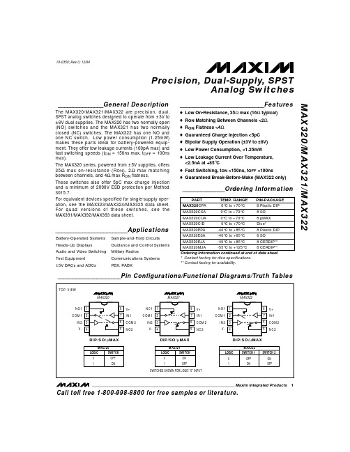
MAX320-MAX322中文资料
ELECTRICAL CHARACTERISTICS
(V+ = +5V ±10%, V- = -5V ±10%, VINH = 3.5V, VINL = 2.5V, TA = TMIN to TMAX, unless otherwise noted.)
PARAMETER ANALOG SWITCH Analog Signal Range
For equivalent devices specified for single-supply operation, see the MAX323/MAX324/MAX325 data sheet. For quad versions of these switches, see the MAX391/MAX392/MAX393 data sheet.
Plastic DIP (derate 9.09mW/°C above +70°C) .............727mW Narrow SO (derate 5.88mW/°C above +70°C) .............471mW
µMAX (derate 4.10mW/°C above +70°C) .....................330mW CERDIP (derate 8.00mW/°C above +70°C) ..................640mW Operating Temperature Ranges MAX32_C_ _ ........................................................0°C to +70°C MAX32_E_ _......................................................-40°C to +85°C MAX32_MJA ...................................................-55°C to +125°C Storage Temperature Range .............................-65°C to +150°C Lead Temperature (soldering, 10sec) .............................+300°C
MAX465中文资料

PART
DESCRIPΒιβλιοθήκη IONMAX463 MAX464 MAX465 MAX466 MAX467 MAX468 MAX469 MAX470
Triple RGB Switch & Buffer Quad RGB Switch & Buffer Triple RGB Switch & Buffer Quad RGB Switch & Buffer Triple Video Buffer Quad Video Buffer Triple Video Buffer Quad Video Buffer
Continuous Power Dissipation (TA = +70°C) 16-Pin Plastic DIP (derate 22.22mW/°C above +70°C) ....1778mW 16-Pin Wide SO (derate 20.00mW/°C above +70°C) .......1600mW
The MAX463–MAX470 series of two-channel, triple/quad buffered video switches and video buffers combines high-accuracy, unity-gain-stable amplifiers with high-performance video switches. Fast switching time and low differential gain and phase error make this series of switches and buffers ideal for all video applications. The devices are all specified for ±5V supply operation with inputs and outputs as high as ±2.5V when driving 150Ω loads (75Ω back-terminated cable).
1SMA5918BT3G中文资料

1SMA5913BT3 Series1.5 Watt PlasticSurface MountZener Voltage RegulatorsThis complete new line of 1.5 Watt Zener Diodes offers the following advantages.Features•Standard Zener Breakdown V oltage Range − 3.3 V to 68 V •ESD Rating of Class 3 (>16 kV) per Human Body Model •Flat Handling Surface for Accurate Placement •Package Design for Top Slide or Bottom Circuit Board Mounting •Low Profile Package•Ideal Replacement for MELF Packages•Pb−Free Packages are AvailableMechanical Characteristics:CASE:V oid-free, transfer-molded plasticFINISH:All external surfaces are corrosion resistant with readily solderable leadsMAXIMUM CASE TEMPERATURE FOR SOLDERING PURPOSES: 260°C for 10 secondsPOLARITY:Cathode indicated by molded polarity notch or cathode bandFLAMMABILITY RATING:UL 94 V−0 @ 0.125 inMAXIMUM RATINGSRating Symbol Value UnitDC Power Dissipation @ T L = 75°C, Measured Zero Lead Length (Note 1) Derate above 75°CThermal Resistance, Junction−to−LeadP DR q JL1.52050WmW/°C°C/WDC Power Dissipation @ T A = 25°C (Note 2) Derate above 25°CThermal Resistance, Junction−to−AmbientP DR q JA0.54.0250WmW/°C°C/WOperating and Storage Temperature Range T J, T stg−65 to+150°CStresses exceeding Maximum Ratings may damage the device. Maximum Ratings are stress ratings only. Functional operation above the Recommended Operating Conditions is not implied. Extended exposure to stresses above the Recommended Operating Conditions may affect device reliability.1. 1 in square copper pad, FR−4 board.2.FR−4 Board, using ON Semiconductor minimum recommended footprint.Device Package Shipping†ORDERING INFORMATION1SMA59xxBT3SMA5000/Tape & Reel1SMA59xxBT3G SMA(Pb−Free)5000/Tape & Reel†For information on tape and reel specifications, including part orientation and tape sizes, please refer to our T ape and Reel Packaging Specifications Brochure, BRD8011/D.See specific marking information in the device marking column of the Electrical Characteristics table on page 2 of this data sheet.DEVICE MARKING INFORMATIONELECTRICAL CHARACTERISTICS (T A = 25°C unlessotherwise noted, V F = 1.5 V Max. @ I F = 200 mA for all types)Symbol ParameterV Z Reverse Zener Voltage @ I ZT I ZT Reverse CurrentZ ZT Maximum Zener Impedance @ I ZT I ZK Reverse CurrentZ ZK Maximum Zener Impedance @ I ZK I R Reverse Leakage Current @ V R V R Reverse Voltage I F Forward Current V F Forward Voltage @ I F I ZMMaximum DC Zener CurrentELECTRICAL CHARACTERISTICS (T A = 25°C unless otherwise noted, V F = 1.5 V Max. @ I F = 200 mA for all types)Device* (Note 3)Device Marking Zener Voltage (Note 4)Zener Impedance Leakage CurrentI ZM V Z (Volts)@ I ZT Z ZT @ I ZTZ ZK @ I ZK I R @ V R Min Nom Max mA W W mA m A Volts mA(dc)1SMA5913BT3, G 813B 3.13 3.3 3.47113.610500 1.050 1.04551SMA5914BT3, G 814B 3.42 3.6 3.78104.29.0500 1.035.5 1.04171SMA5915BT3, G 815B 3.70 3.9 4.1096.17.5500 1.012.5 1.03851SMA5916BT3, G 816B 4.08 4.3 4.5287.2 6.0500 1.0 2.5 1.03491SMA5917BT3, G 817B 4.46 4.7 4.9479.8 5.0500 1.0 2.5 1.53191SMA5918BT3, G 818B 4.84 5.1 5.3673.5 4.0350 1.0 2.5 2.02941SMA5919BT3, G 819B 5.32 5.6 5.8866.9 2.0250 1.0 2.5 3.02681SMA5920BT3, G 820B 5.89 6.2 6.5160.5 2.0200 1.0 2.5 4.02421SMA5921BT3, G 821B 6.46 6.87.1455.1 2.5200 1.0 2.5 5.22211SMA5922BT3, G 822B 7.127.57.8850 3.04000.5 2.5 6.02001SMA5923BT3, G 823B 7.798.28.6145.7 3.54000.5 2.5 6.51831SMA5924BT3, G 824B 8.649.19.5641.2 4.05000.5 2.57.01651SMA5925BT3, G 825B 9.51010.537.5 4.55000.25 2.58.01501SMA5926BT3, G 826B 10.451111.5534.1 5.55500.250.58.41361SMA5927BT3, G 827B 11.41212.631.2 6.55500.250.59.11251SMA5928BT3, G 828B 12.351313.6528.87.05500.250.59.91151SMA5929BT3, G 829B 14.251515.75259.06000.250.511.41001SMA5930BT3, G 830B 15.21616.823.4106000.250.512.2941SMA5931BT3, G 831B 17.11818.920.8126500.250.513.7831SMA5932BT3, G 832B 19202118.7146500.250.515.2751SMA5933BT3, G 833B 20.92223.11717.56500.250.516.7681SMA5934BT3, G 834B 22.82425.215.6197000.250.518.2631SMA5935BT3, G 835B 25.652728.3513.9237000.250.520.6561SMA5936BT3, G 836B 28.53031.512.5267500.250.522.8501SMA5937BT3, G 837B 31.353334.6511.4338000.250.525.1451SMA5938BT3, G 838B 34.23637.810.4388500.250.527.4421SMA5939BT3, G 839B 37.053940.959.6459000.250.529.7381SMA5940BT3, G840B40.854345.158.7539500.250.532.7351SMA5941BT3, G 841B 44.654749.358.06710000.250.535.8321SMA5942BT3, G 842B 48.455153.557.37011000.250.538.8291SMA5943BT3, G 843B 53.25658.8 6.78613000.250.542.6271SMA5944BT3, G 844B 58.96265.1 6.010015000.250.547.1241SMA5945BT3, G 845B 64.66871.4 5.512017000.250.551.7223.Tolerance and Voltage Regulation Designation − The type number listed indicates a tolerance of ±5%.4.V Z limits are to be guaranteed at thermal equilibrium.*The “G” suffix indicates Pb−Free package available.Figure 1. Steady State Power DeratingFigure 2. V Z − 3.3 thru 10 VoltsT, TEMPERATURE (°C)Figure 3. V Z = 12 thru 68 VoltsP D , M A X I M U MP O W E R D I S S I P A T I O N (W A T T S )I Z , Z E N E R C U R R E N T (m A )Z Z , D Y N A M I C I M P ED A N CE (O H M S )1002468101010.1V Z , ZENER VOLTAGE (VOLTS)1001010.1010203040V Z , ZENER VOLTAGE (VOLTS)V Z , ZENER VOLTAGE (VOLTS)1001050Figure 4. Zener Voltage − 3.3 to 12 VoltsFigure 5. Zener Voltage − 12 to 68 Volts Figure 6. Effect of Zener VoltageI Z , Z E N E R C U R R E N T (m A )6070801086420−2−4V Z , ZENER VOLTAGE (VOLTS), T E M P E R A T U R E C O E F F I C I E N T (m V / C )°θV Z 10070503020101020305070100V Z , ZENER VOLTAGE (VOLTS), T E M P E R A T U R E C O E F F I C I E N T (m V / C )°θV ZPACKAGE DIMENSIONSSMACASE 403D−02ISSUE Cǒmm inchesǓSCALE 8:1*For additional information on our Pb−Free strategy and solderingdetails, please download the ON Semiconductor Soldering and Mounting Techniques Reference Manual, SOLDERRM/D.SOLDERING FOOTPRINT*DIM A MIN NOM MAX MINMILLIMETERS1.912.16 2.410.075INCHES A10.050.100.150.002b 1.27 1.45 1.630.050c 0.150.280.410.006D 2.29 2.60 2.920.090E 4.06 4.32 4.570.160L0.761.14 1.520.0300.0850.0950.0040.0060.0570.0640.0110.0160.1030.1150.1700.1800.0450.060NOM MAX 4.83 5.21 5.590.1900.2050.220H E STYLE 1:PIN 1.CATHODE (POLARITY BAND)2.ANODENOTES:1.DIMENSIONING AND TOLERANCING PER ANSI Y14.5M, 1982.2.CONTROLLING DIMENSION: INCH.3.403D−01 OBSOLETE, NEW STANDARD IS 403D−02.ON Semiconductor and are registered trademarks of Semiconductor Components Industries, LLC (SCILLC). SCILLC reserves the right to make changes without further notice to any products herein. SCILLC makes no warranty, representation or guarantee regarding the suitability of its products for any particular purpose, nor does SCILLC assume any liability arising out of the application or use of any product or circuit, and specifically disclaims any and all liability, including without limitation special, consequential or incidental damages.“Typical” parameters which may be provided in SCILLC data sheets and/or specifications can and do vary in different applications and actual performance may vary over time. All operating parameters, including “Typicals” must be validated for each customer application by customer’s technical experts. SCILLC does not convey any license under its patent rights nor the rights of others. SCILLC products are not designed, intended, or authorized for use as components in systems intended for surgical implant into the body, or other applications intended to support or sustain life, or for any other application in which the failure of the SCILLC product could create a situation where personal injury or death may occur. Should Buyer purchase or use SCILLC products for any such unintended or unauthorized application, Buyer shall indemnify and hold SCILLC and its officers, employees, subsidiaries, affiliates,and distributors harmless against all claims, costs, damages, and expenses, and reasonable attorney fees arising out of, directly or indirectly, any claim of personal injury or death associated with such unintended or unauthorized use, even if such claim alleges that SCILLC was negligent regarding the design or manufacture of the part. SCILLC is an Equal Opportunity/Affirmative Action Employer. This literature is subject to all applicable copyright laws and is not for resale in any manner.PUBLICATION ORDERING INFORMATION。
MEMORY存储芯片MAX485EESA中文规格书

General Description The MAX481E, MAX483E, MAX485E, MAX487E–MAX491E, and MAX1487E are low-power transceivers for RS-485 and RS-422 communications in harsh environ-ments. Each driver output and receiver input is protected against ±15kV electro-static discharge (ESD) shocks, without latchup. These parts contain one driver and one receiver. The MAX483E, MAX487E, MAX488E, and MAX489E feature reduced slew-rate drivers that minimize EMI and reduce reflections caused by improperly termi-nated cables, thus allowing error-free data transmission up to 250kbps. The driver slew rates of the MAX481E, MAX485E, MAX490E, MAX491E, and MAX1487E are not limited, allowing them to transmit up to 2.5Mbps.These transceivers draw as little as 120µA supply cur-rent when unloaded or when fully loaded with disabled drivers (see Selector Guide). Additionally, the MAX481E, MAX483E, and MAX487E have a low-current shutdown mode in which they consume only 0.5µA. All parts oper-ate from a single +5V supply.Drivers are short-circuit current limited, and are protected against excessive power dissipation by thermal shutdown circuitry that places their outputs into a high-impedance state. The receiver input has a fail-safe feature that guar-antees a logic-high output if the input is open circuit.The MAX487E and MAX1487E feature quarter-unit-load receiver input impedance, allowing up to 128 trans-ceivers on the bus. The MAX488E–MAX491E are designed for full-duplex communications, while the MAX481E, MAX483E, MAX485E, MAX487E, and MAX1487E are designed for half-duplex applications. For applications that are not ESD sensitive see the pin-and function-compatible MAX481, MAX483, MAX485, MAX487–MAX491, and MAX1487.Applications Low-Power RS-485 TransceiversLow-Power RS-422 TransceiversLevel TranslatorsTransceivers for EMI-Sensitive ApplicationsIndustrial-Control Local Area NetworksNext-Generation Device Features ♦For Fault-Tolerant Applications:MAX3430: ±80V Fault-Protected, Fail-Safe, 1/4-Unit Load, +3.3V, RS-485 TransceiverMAX3080–MAX3089: Fail-Safe, High-Speed(10Mbps), Slew-Rate-Limited, RS-485/RS-422Transceivers♦For Space-Constrained Applications:MAX3460–MAX3464: +5V, Fail-Safe, 20Mbps,Profibus, RS-485/RS-422 TransceiversMAX3362: +3.3V, High-Speed, RS-485/RS-422Transceiver in a SOT23 PackageMAX3280E–MAX3284E: ±15kV ESD-Protected,52Mbps, +3V to +5.5V, SOT23, RS-485/RS-422True Fail-Safe ReceiversMAX3030E–MAX3033E: ±15kV ESD-Protected,+3.3V, Quad RS-422 Transmitters♦For Multiple Transceiver Applications:MAX3293/MAX3294/MAX3295: 20Mbps, +3.3V,SOT23, RS-485/RS-422 Transmitters♦For Fail-Safe Applications:MAX3440E–MAX3444E: ±15kV ESD-Protected,±60V Fault-Protected, 10Mbps, Fail-SafeRS-485/J1708 Transceivers♦For Low-Voltage Applications:MAX3483E/MAX3485E/MAX3486E/MAX3488E/MAX3490E/MAX3491E: +3.3V Powered, ±15kVESD-Protected, 12Mbps, Slew-Rate-Limited,True RS-485/RS-422 Transceivers±15kV ESD-Protected, Slew-Rate-Limited, Low-Power, RS-485/RS-422 TransceiversOrdering InformationOrdering Information continued at end of data sheet.Selector Guide appears at end of data sheet.±15kV ESD-Protected, Slew-Rate-Limited,Low-Power, RS-485/RS-422 Transceivers__________Function Tables (MAX481E/MAX483E/MAX485E/MAX487E/MAX1487E)Table 1. TransmittingTable 2. Receivingneers developed state-of-the-art structures to protect these pins against ESD of ±15kV without damage. The ESD structures withstand high ESD in all states: normal operation, shutdown, and powered down. After an ESD event, Maxim’s MAX481E, MAX483E, MAX485E, MAX487E–MAX491E, and MAX1487E keep working without latchup.ESD protection can be tested in various ways; the transmitter outputs and receiver inputs of this product family are characterized for protection to ±15kV using the Human Body Model.Other ESD test methodologies include IEC10004-2 con-tact discharge and IEC1000-4-2 air-gap discharge (for-merly IEC801-2).ESD Test ConditionsESD performance depends on a variety of conditions.Contact Maxim for a reliability report that documents test set-up, test methodology, and test results.Human Body ModelF igure 4 shows the Human Body Model, and F igure 5shows the current waveform it generates when dis-charged into a low impedance. This model consists of a 100pF capacitor charged to the ESD voltage of inter-est, which is then discharged into the test device through a 1.5k Ωresistor.IEC1000-4-2The IEC1000-4-2 standard covers ESD testing and per-formance of finished equipment; it does not specifically refer to integrated circuits (Figure 6).MAX481E/MAX483E/MAX485E/ MAX487E–MAX491E/MAX1487E__________Applications InformationThe MAX481E/MAX483E/MAX485E/MAX487E–MAX491E and MAX1487E are low-power transceivers for RS-485 and RS-422 communications. These “E” versions of the MAX481, MAX483, MAX485, MAX487–MAX491, and MAX1487 provide extra protection against ESD. The rugged MAX481E, MAX483E, MAX485E, MAX497E–MAX491E, and MAX1487E are intended for harsh envi-ronments where high-speed communication is important. These devices eliminate the need for transient suppres-sor diodes and the associated high capacitance loading.The standard (non-“E”) MAX481, MAX483, MAX485, MAX487–MAX491, and MAX1487 are recommended for applications where cost is critical.The MAX481E, MAX485E, MAX490E, MAX491E, and MAX1487E can transmit and receive at data rates up to 2.5Mbps, while the MAX483E, MAX487E, MAX488E, and MAX489E are specified for data rates up to 250kbps. The MAX488E–MAX491E are full-duplex transceivers, while the MAX481E, MAX483E, MAX487E, and MAX1487E are half-duplex. In addition, driver-enable (DE) and receiver-enable (RE) pins are included on the MAX481E, MAX483E, MAX485E, MAX487E, MAX489E, MAX491E, and MAX1487E. When disabled, the driver and receiver outputs are high impedance.±15kV ESD ProtectionAs with all Maxim devices, ESD-protection structures are incorporated on all pins to protect against electro-static discharges encountered during handling and assembly. The driver outputs and receiver inputs have extra protection against static electricity. Maxim’s engi-±15kV ESD-Protected, Slew-Rate-Limited,Low-Power, RS-485/RS-422 TransceiversFigure 6. IEC1000-4-2 ESD Test ModelFigure 8. Driver DC Test LoadFigure 7. IEC1000-4-2 ESD Generator Current WaveformFigure 9. Receiver Timing Test LoadFigure 4. Human Body ESD Test ModelFigure 5. Human Body Model Current WaveformMAX481E/MAX483E/MAX485E/ MAX487E–MAX491E/MAX1487E±15kV ESD-Protected, Slew-Rate-Limited,Low-Power, RS-485/RS-422 Transceiversdelay times. Typical propagation delays are shown in Figures 19–22 using Figure 18’s test circuit.The difference in receiver delay times, t PLH - t PHL , is typically under 13ns for the MAX481E, MAX485E,MAX490E, MAX491E, and MAX1487E, and is typically less than 100ns for the MAX483E and MAX487E–MAX489E.The driver skew times are typically 5ns (10ns max) for the MAX481E, MAX485E, MAX490E, MAX491E, and MAX1487E, and are typically 100ns (800ns max) for the MAX483E and MAX487E–MAX489E.Typical ApplicationsThe MAX481E, MAX483E, MAX485E, MAX487E–MAX491E, and MAX1487E transceivers are designed for bidirectional data communications on multipoint bus transmission lines. F igures 25 and 26 show typical net-work application circuits. These parts can also be used as line repeaters, with cable lengths longer than 4000 feet.To minimize reflections, the line should be terminated at both ends in its characteristic impedance, and stub lengths off the main line should be kept as short as possi-ble. The slew-rate-limited MAX483E and MAX487E–MAX489E are more tolerant of imperfect termination.Bypass the V CC pin with 0.1µF.Isolated RS-485For isolated RS-485 applications, see the MAX253 and MAX1480 data sheets.Line Length vs. Data RateThe RS-485/RS-422 standard covers line lengths up to 4000 feet. Figures 23 and 24 show the system differen-tial voltage for the parts driving 4000 feet of 26AWG twisted-pair wire at 110kHz into 100Ωloads.Figure 18. Receiver Propagation Delay Test CircuitIt takes the drivers and receivers longer to become enabled from the low-power shutdown state (t ZH(SHDN ), t ZL(SHDN)) than from the operating mode (t ZH , t ZL ). (The parts are in operating mode if the RE, DE inputs equal a logical 0,1 or 1,1 or 0, 0.)Driver Output ProtectionExcessive output current and power dissipation caused by faults or by bus contention are prevented by two mechanisms. A foldback current limit on the output stage provides immediate protection against short circuits over the whole common-mode voltage range (see Typical Operating Characteristics ). In addition, a thermal shut-down circuit forces the driver outputs into a high-imped-ance state if the die temperature rises excessively.Propagation DelayMany digital encoding schemes depend on the differ-。
max24033emy+t的规格书
max24033emy+t的规格书规格书:max24033emy+t一、产品介绍:max24033emy+t是一款高度集成的4通道电源管理IC,它主要用于工业控制系统、通信设备和数据中心等领域的电源管理。
该产品采用优质的半导体材料和先进的封装工艺,具有稳定可靠的性能和高效省电的特点。
二、产品特点:1.高度集成:max24033emy+t集成了4个高性能电源管理通道,包括电池充电管理、DC-DC转换器和电源监控等功能,可满足多种应用的需求。
2.宽输入电压范围:max24033emy+t支持广泛的输入电压范围,从3.5V到28V,能适应不同电源供应的要求。
3.高效节能:max24033emy+t采用了先进的能量管理技术,具有高效节能的特点,可以最大程度地减少能源浪费。
4.低功耗待机模式:max24033emy+t在待机模式下,功耗极低,能有效延长电池使用寿命。
5.温度保护:max24033emy+t具有自动温度保护功能,可在过热时自动停止工作,保护电路不受损坏。
6.电池管理:max24033emy+t支持电池充电和放电管理,能确保电池使用的安全和稳定性。
三、应用领域:max24033emy+t广泛应用于各种工业控制系统、通信设备和数据中心等领域,如智能家居、自动化控制、无线通信设备、数据存储等。
四、主要性能参数:1.输入电压范围:3.5V-28V2.输出电压范围:1.5V-16V3.输出电流范围:0A-3A4.工作温度范围:-40℃~85℃5.封装形式:QFN封装五、产品优势:1.优质材料:max24033emy+t采用优质的半导体材料和先进的封装工艺,保证了产品的稳定性和可靠性。
2.高效节能:max24033emy+t采用了先进的能量管理技术,具有高效节能的特点,能最大程度地减少能源浪费。
3.宽电压范围:max24033emy+t支持广泛的输入电压范围,能适应不同电源供应的要求。
4.多通道设计:max24033emy+t具有4个独立的电源管理通道,可满足多种应用的需求。
MAX713中文资料
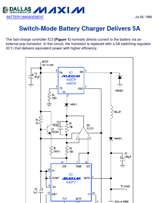
BATTERY MANAGEMENT Jul 09, 1998 Switch-Mode Battery Charger Delivers 5AThe fast-charge controller IC3 (Figure 1) normally directs current to the battery via an external pnp transistor. In this circuit, the transistor is replaced with a 5A switching regulator (IC1) that delivers equivalent power with higher efficiency.Figure 1. By controlling the PWM duty cycle of switching regulator IC1, the fast-charge controller (IC3) makes efficient delivery of the battery's charging current.IC1 is a 5A buck switching regulator whose output is configured as a current source. Its internal power switch (an npn transistor) is relatively efficient because V CE(SAT) is small in comparison with the 15V-to-40V inputs. (For applications that require 2A or less, the low-saturation, non-Darlington power switch of a MAX726 offers better efficiency.)R6 senses the battery-charging current and enables IC3 to generate an analog drive signal at DRV. The signal is first attenuated by the op amp to assure stability by reducing gain in the control loop. It then drives IC1's compensation pin (VC), which gives direct access to the internal PWM comparator. IC3 thus controls the charging current via the PWM duty cycle of IC1. The Q1 buffer provides current to the DRV input.Loop stability is also determined by the feedback loop's dominant pole, set by C4 at the CC terminal of IC3. If you increase the value of the battery filter capacitor (C5), you should make a proportional increase in the value of C4. Lower values, however, assure good transient response. If your application produces load transients during the fast-charge cycle, check the worst-case response to a load step. To assure proper termination of the charge, battery voltage should settle within 2msec to 5mV times N (where N is the number of battery cells). More InformationMAX713:QuickView-- Full (PDF) Data Sheet-- Free Samples。
- 1、下载文档前请自行甄别文档内容的完整性,平台不提供额外的编辑、内容补充、找答案等附加服务。
- 2、"仅部分预览"的文档,不可在线预览部分如存在完整性等问题,可反馈申请退款(可完整预览的文档不适用该条件!)。
- 3、如文档侵犯您的权益,请联系客服反馈,我们会尽快为您处理(人工客服工作时间:9:00-18:30)。
General Description The MAX6381–MAX6390 microprocessor (µP) supervisory circuits monitor power-supply voltages from +1.8V to +5.0V while consuming only 3µA of supply current at +1.8V. Whenever V CC falls below the factory-set reset thresholds, the reset output asserts and remains assert-ed for a minimum reset timeout period after V CC rises above the reset threshold. Reset thresholds are available from +1.58V to +4.63V, in approximately 100mV incre-ments. Seven minimum reset timeout delays ranging from 1ms to 1200ms are available.The MAX6381/MAX6384/MAX6387 have a push-pull active-low reset output. The MAX6382/MAX6385/ MAX6388 have a push-pull active-high reset output, and the MAX6383/MAX6386/MAX6389/MAX6390 have an open-drain active-low reset output. The MAX6384/MAX6385/MAX6386 also feature a debounced manual reset input (with internal pullup resistor). The MAX6387/MAX6388/MAX6389 have an auxiliary input for monitoring a second voltage. The MAX6390 offers a manual reset input with a longer V CC reset timeout period (1120ms or 1200ms) and a shorter manual reset timeout (140ms or 150ms).The MAX6381/MAX6382/MAX6383 are available in 3-pin SC70 and6-pinµDFN packages and the MAX6384–MAX6390 are available in 4-pin SC70 andFeatures♦Factory-Set Reset Threshold Voltages Rangingfrom +1.58V to +4.63V in Approximately 100mVIncrements♦±2.5% Reset Threshold Accuracy OverTemperature (-40°C to +125°C)♦Seven Reset Timeout Periods Available: 1ms,20ms, 140ms, 280ms, 560ms, 1120ms,1200ms (min)♦3 Reset Output OptionsActive-Low Push-PullActive-High Push-PullActive-Low Open-Drain♦Reset Output State Guaranteed ValidDown to V CC= 1V♦Manual Reset Input (MAX6384/MAX6385/MAX6386)♦Auxiliary RESET IN(MAX6387/MAX6388/MAX6389)♦V CC Reset Timeout (1120ms or 1200ms)/ManualReset Timeout (140ms or 150ms) (MAX6390)♦Negative-Going V CC Transient Immunity♦Low Power Consumption of 6µA at +3.6Vand 3µA at +1.8V♦Pin Compatible withMAX809/MAX810/MAX803/MAX6326/MAX6327/MAX6328/MAX6346/MAX6347/MAX6348,and MAX6711/MAX6712/MAX6713♦Tiny 3-Pin/4-Pin SC70 and 6-Pin µDFN PackagesMAX6381–MAX6390 SC70/µDFN, Single/Dual Low-Voltage,Low-Power µP Reset Circuits ________________________________________________________________Maxim Integrated Products1Pin Configurations19-1839; Rev 4; 4/07Ordering InformationOrdering Information continued at end of data sheet.Typi cal Operati ng Ci rcui t appears at end of data sheet.Selector Guide appears at end of data sheet.after "XR", "XS", or "LT." Insert reset timeout delay (see ResetTimeout Delay table) after "D" to complete the part number.Sample stock is generally held on standard versions only (seeStandard Versions table). Standard versions have an orderincrement requirement of 2500 pieces. Nonstandard versionshave an order increment requirement of 10,000 pieces.Contact factory for availability of nonstandard versions.+Denotes a lead-free package.For pricing, delivery, and ordering information,please contact Maxim Direct at 1-888-629-4642,or visit Maxim’s website at .ComputersControllersIntelligent InstrumentsCritical µP and µCPower MonitoringPortable/Battery-Powered EquipmentDual Voltage SystemsM A X 6381–M A X 6390SC70/µDFN, Single/Dual Low-Voltage, Low-Power µP Reset CircuitsABSOLUTE MAXIMUM RATINGSELECTRICAL CHARACTERISTICS(V CC = full range, T A = -40°C to +125°C, unless otherwise specified. Typical values are at T A = +25°C.) (Note 1)Stresses beyond those listed under “Absolute Maximum Ratings” may cause permanent damage to the device. These are stress ratings only, and functional operation of the device at these or any other conditions beyond those indicated in the operational sections of the specifications is not implied. Exposure to absolute maximum rating conditions for extended periods may affect device reliability.V CC to GND..........................................................-0.3V to +6.0V RESET Open-Drain Output....................................-0.3V to +6.0V RESET , RESET (push-pull output)..............-0.3V to (V CC + 0.3V)MR , RESET IN.............................................-0.3V to (V CC + 0.3V)Input Current (V CC ).............................................................20mA Output Current (all pins).....................................................20mAContinuous Power Dissipation (T A = +70°C)3-Pin SC70 (derate 2.9mW/°C above +70°C)..............235mW 4-Pin SC70 (derate 3.1mW/°C above +70°C)..............245mW 6-Pin µDFN (derate 2.1mW/°C above +70°C)..........167.7mW Operating Temperature Range .........................-40°C to +125°C Storage Temperature Range.............................-65°C to +150°C Lead Temperature (soldering, 10s).................................+300°CMAX6381–MAX6390SC70/µDFN, Single/Dual Low-Voltage,Low-Power µP Reset Circuits_______________________________________________________________________________________3M A X 6381–M A X 6390SC70/µDFN, Single/Dual Low-Voltage, Low-Power µP Reset Circuits 4______________________________________________________________________________________Typical Operating Characteristics(T A = +25°C, unless otherwise noted.)215436789-40-105-25203550658095110125SUPPLY CURRENT vs. TEMPERATURE(NO LOAD)TEMPERATURE (°C)S U P P L Y C U R R E N T (µA )25292735333137394143-40-105-25203550658095110125POWER-DOWN RESET DELAYvs. TEMPERATURETEMPERATURE (°C)P O W E R -D O W N R E S E T D E L A Y (µs )0.940.980.961.021.001.061.041.08-40-10520-253550658095110125NORMALIZED POWER-UP RESET TIMEOUTvs. TEMPERATUREM A X 6381/90 t o c 03TEMPERATURE (°C)N O R M A L I Z E D R E S E T T I M E O U T P E R I O D0.9900.9851.0150.9950.9901.0001.0051.0101.020-40-10520-253550958011065125M A X 6381/90 t o c 04TEMPERATURE (°C)N O R M A L I Z E D R E S E T TH R E S H O L D NORMALIZED RESET THRESHOLDvs. TEMPERATURE00.40.20.80.61.01.2063912OUTPUT-VOLTAGE LOW vs. SINK CURRENTI SINK (mA)V O L (V )01.00.52.01.52.53.00500750250100012501500OUTPUT-VOLTAGE HIGH vs. SOURCE CURRENTI SOURCE (µA)V O H (V )45001100010010MAXIMUM TRANSIENT DURATION vs. RESET COMPARATOR OVERDRIVE15050350250500200100400300RESET COMPARATOR OVERDRIVE, V TH - V CC (mV)M A X I M U M T R A N S I E N T D U R A T I O N (µs )3.53.93.74.54.34.14.74.95.35.15.5-40-105-25203550658095110125RESET IN TO RESET DELAYvs. TEMPERATUREM A X 6381/90 t o c 08TEMPERATURE (°C)R E S E T I N D E L A Y (µs )MAX6381–MAX6390SC70/µDFN, Single/Dual Low-Voltage,Low-Power µP Reset CircuitsPin DescriptionM A X 6381–M A X 6390SC70/µDFN, Single/Dual Low-Voltage, Low-Power µP Reset Circuits 6_______________________________________________________________________________________Detailed DescriptionRESET OutputA µP reset input starts the µP in a known state. These µP supervisory circuits assert reset to prevent code execution errors during power-up, power-down, or brownout conditions.Reset asserts when V CC is below the reset threshold;once V CC exceeds the reset threshold, an internal timer keeps the reset output asserted for the reset timeout period. After this interval, reset output deasserts. Reset output is guaranteed to be in the correct logic state for V CC ≥1V.Manual Reset Input (MAX6384/MAX6385/MAX6386/MAX6390)Many µP-based products require manual reset capabil-ity, allowing the operator, a test technician, or external logic circuitry to initiate a reset. A logic low on MR asserts reset. Reset remains asserted while MR is low,and for the reset active timeout period (t RP ) after MR returns high. This input has an internal 63k Ωpullup resistor (1.56k Ωfor MAX6390), so it can be left uncon-nected if it is not used. MR can be driven with TTL or CMOS logic levels, or with open-drain/collector outputs.Connect a normally open momentary switch from MR to G ND to create a manual-reset function; external debounce circuitry is not required. If MR is driven from long cables or if the device is used in a noisy environ-ment, connecting a 0.1µF capacitor from MR to G ND provides additional noise immunity.RESET IN Comparator(MAX6387/MAX6388/MAX6389)RESET IN is compared to an internal +1.27V reference.If the voltage at RESET IN is less than 1.27V, reset asserts. Use the RESET IN comparator as a user-adjustable reset detector or as a secondary power-sup-ply monitor by implementing a resistor-divider at RESET IN (shown in Figure 1). Reset asserts when either V CC or RESET IN falls below its respective threshold volt-age. Use the following equation to set the threshold:V INTH = V THRST (R1/R2 + 1)where V THRST = +1.27V. To simplify the resistor selec-tion, choose a value of R2 and calculate R1:R1 = R2 [(V INTH /V THRST ) - 1]Since the input current at RESET IN is 50nA (max),large values can be used for R2 with no significant loss in accuracy.___________Applications InformationNegative-Going V CC TransientsIn addition to issuing a reset to the µP during power-up,power-down, and brownout conditions, the MAX6381–MAX6390 are relatively immune to short dura-tion negative-going V CC transients (glitches).The Typical Operating Characteristics section shows the Maximum Transient Durations vs. Reset Comparator Overdrive, for which the MAX6381–MAX6390 do not generate a reset pulse. This graph was generated usinga negative-going pulse applied to V CC , starting above the actual reset threshold and ending below it by the magnitude indicated (reset comparator overdrive). The graph indicates the typical maximum pulse width a neg-ative-going V CC transient may have without causing a reset pulse to be issued. As the magnitude of the tran-sient increases (goes farther below the reset threshold),the maximum allowable pulse width decreases. A 0.1µF capacitor mounted as close as possible to V CC provides additional transient immunity.Ensuring a Valid RESET Output Down to V CC = 0VThe MAX6381–MAX6390 are guaranteed to operate properly down to V CC = 1V. In applications that require valid reset levels down to V CC = 0V, a pulldown resistor to active-low outputs (push/pull only, Figure 2) and a pullup resistor to active-high outputs (push/pull only)will ensure that the reset line is valid while the reset out-put can no longer sink or source current. This schemedoes not work with the open-drain outputs of the MAX6383/MAX6386/MAX6389/MAX6390. The resistor value used is not critical, but it must be small enough not to load the reset output when V CC is above the reset threshold. For most applications, 100k Ωis ade-quate.MAX6381–MAX6390SC70/µDFN, Single/Dual Low-Voltage,Low-Power µP Reset Circuits_______________________________________________________________________________________7M A X 6381–M A X 6390SC70/µDFN, Single/Dual Low-Voltage, Low-Power µP Reset Circuits 8_______________________________________________________________________________________Selector GuideOrdering Information (continued)Note:Insert reset threshold suffix (see Reset Threshold table)after "XR", "XS", or "LT." Insert reset timeout delay (see Reset Timeout Delay table) after "D" to complete the part number.Sample stock is generally held on standard versions only (see Standard Versions table). Standard versions have an order increment requirement of 2500 pieces. Nonstandard versions have an order increment requirement of 10,000 pieces.Contact factory for availability of nonstandard versions.*MAX6390 is available with D4 or D7 timing only.+Denotes a lead-free package.MAX6381–MAX6390SC70/µDFN, Single/Dual Low-Voltage,Low-Power µP Reset Circuits_______________________________________________________________________________________9Chip InformationTRANSISTOR COUNT: 647PROCESS: BiCMOSPin Configurations (continued)M A X 6381–M A X 6390SC70/µDFN, Single/Dual Low-Voltage, Low-Power µP Reset Circuits 10______________________________________________________________________________________Package Information(The package drawing(s) in this data sheet may not reflect the most current specifications. For the latest package outline information,go to /packages .)MAX6381–MAX6390SC70/µDFN, Single/Dual Low-Voltage,Low-Power µP Reset Circuits______________________________________________________________________________________11Package Information (continued)(The package drawing(s) in this data sheet may not reflect the most current specifications. For the latest package outline information,go to /packages .)M A X 6381–M A X 6390SC70/µDFN, Single/Dual Low-Voltage, Low-Power µP Reset Circuits 12______________________________________________________________________________________Package Information (continued)(The package drawing(s) in this data sheet may not reflect the most current specifications. For the latest package outline information,go to /packages .)SC70/µDFN, Single/Dual Low-Voltage,Low-Power µP Reset CircuitsMaxim cannot assume responsibility for use of any circuitry other than circuitry entirely embodied in a Maxim product. No circuit patent licenses are implied. Maxim reserves the right to change the circuitry and specifications without notice at any time.Maxim Integrated Products, 120 San Gabriel Drive, Sunnyvale, CA 94086 408-737-7600____________________13©2007 Maxim Integrated Productsis a registered trademark of Maxim Integrated Products, Inc.MAX6381–MAX6390Package Information (continued)(The package drawing(s) in this data sheet may not reflect the most current specifications. For the latest package outline information,go to /packages .)Revision HistoryPages changed at Rev 4: Title on all pages, 1, 2, 5,7–13。