GS864036T-200I中文资料
Testo 德图红外热像仪 产品手册

德图红外热像仪产品手册从基础到高端,全面适用于各行各业国德制造2精密型红外热像仪德图 testo 8833德图红外热像仪产品4德图红外热像仪产品一览testo 883320 x 240 640 x 480–可选功能备注:不具备* 如需订购帧频为 33 Hz 或 27 Hz 热像仪,请与德图官方联系。
5什么是红外热像仪?所有温度在绝对零度(约-273 ℃)以上的物体,都会因自身的分子运动而辐射红外线。
红外热像仪可以将这些人眼无法看到的红外线转换成为电信号,将以各种不同颜色表示不同温度的可视图像显示出来。
通过图像,可以迅速便捷地检测整个温度面,并识别高低温度点,从而可以进行温度的定性与定量分析,如有温度异常则预示将有故障发生。
通过对异常温度的检测,寻找出可能存在的问题,并及早采取相关措施,避免损失的发生。
红外热像仪的应用越来越广泛,在工业领域常用在机械设备的预防性维护及检修电气设备的预防性维护及检修生产过程的质量监控高耗能设备的监控产品研发的实验过程红外热像仪在工业领域的应用优势非接触式测量,无需停工,无需接触,安全快速显示整个温度场的分布,可对测量目标进行整体分析,高效检测显示任何细节部位,发现故障隐患,节约维修成本,降低能源损耗扫描式检测方法,反应灵敏,节约测量时间不同测量任务请选择适合的测量设备全新上市,功能全面,经济适用6德图红外热像仪产品testo 红外热像仪工业领域中电气设备维护的应用应用描述: 热像仪提供对电气设备故障部位或缺陷组件早发现,早判定的检测方法,继而采取针对性的维护或维修措施,避免可能会导致生产停工甚至引发火灾而产生的损失。
应用描述: 触网系统目前在铁路及地铁运行中占据非常重要的作用,保障触网运行是运行人员至关重要的工作,热像仪提供非接触快速扫瞄的远距离测量方式,大面积对触网系统进行扫瞄,有效保障运行。
应用描述: 大多数线路是架空设计,红外热像仪提供远距离的测量方法,简单快捷。
GS864436B-166I中文资料
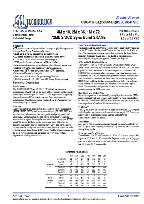
Product PreviewGS864418(B/E)/GS864436(B/E)/GS864472(C)4M x 18, 2M x 36, 1M x 7272Mb S/DCD Sync Burst SRAMs250 MHz –133MHz 2.5 V or 3.3 V V DD 2.5 V or 3.3 V I/O119-, 165-, & 209-Pin BGA Commercial Temp Industrial Temp Features• FT pin for user-configurable flow through or pipeline operation • Single/Dual Cycle Deselect selectable• IEEE 1149.1 JTAG-compatible Boundary Scan• ZQ mode pin for user-selectable high/low output drive • 2.5 V or 3.3 V +10%/–10% core power supply • LBO pin for Linear or Interleaved Burst mode• Internal input resistors on mode pins allow floating mode pins • Default to SCD x18/x36 Interleaved Pipeline mode • Byte Write (BW) and/or Global Write (GW) operation • Internal self-timed write cycle• Automatic power-down for portable applications• JEDEC-standard 119-, 165-, and 209-bump BGA packageFunctional DescriptionApplicationsThe GS864418/36/72 is a 75,497,472-bit high performancesynchronous SRAM with a 2-bit burst address counter. Although of a type originally developed for Level 2 Cache applications supporting high performance CPUs, the device now finds application insynchronous SRAM applications, ranging from DSP main store to networking chip set support.ControlsAddresses, data I/Os, chip enable (E1), address burst control inputs (ADSP, ADSC, ADV), and write control inputs (Bx, BW, GW) are synchronous and are controlled by a positive-edge-triggered clock input (CK). Output enable (G) and power down control (ZZ) are asynchronous inputs. Burst cycles can be initiated with either ADSP or ADSC inputs. In Burst mode, subsequent burst addresses are generated internally and are controlled by ADV. The burst address counter may be configured to count in either linear or interleave order with the Linear Burst Order (LBO) input. The Burst function need not be used. New addresses can be loaded on every cycle with no degradation of chip performance.Flow Through/Pipeline ReadsThe function of the Data Output register can be controlled by the user via the FT mode . Holding the FT mode pin low places the RAM in Flow Through mode, causing output data to bypass the Data Output Register. Holding FT high places the RAM in Pipeline mode, activating the rising-edge-triggered Data Output Register.SCD and DCD Pipelined ReadsThe GS864418/36/72 is a SCD (Single Cycle Deselect) and DCD (Dual Cycle Deselect) pipelined synchronous SRAM. DCD SRAMs pipeline disable commands to the same degree as read commands. SCD SRAMs pipeline deselect commands one stage less than read commands. SCD RAMs begin turning off their outputs immediately after the deselect command has been captured in the input registers. DCD RAMs hold the deselect command for one full cycle and then begin turning off their outputs just after the second rising edge of clock. The user may configure this SRAM for either mode of operation using the SCD mode input.Byte Write and Global WriteByte write operation is performed by using Byte Write enable (BW) input combined with one or more individual byte write signals (Bx). In addition, Global Write (GW) is available for writing all bytes at one time, regardless of the Byte Write control inputs.FLXDrive™The ZQ pin allows selection between high drive strength (ZQ low) for multi-drop bus applications and normal drive strength (ZQ floating or high) point-to-point applications. See the Output Driver Characteristics chart for details.Sleep ModeLow power (Sleep mode) is attained through the assertion (High) of the ZZ signal, or by stopping the clock (CK). Memory data is retained during Sleep mode.Core and Interface VoltagesThe GS864418/36/72 operates on a 2.5 V or 3.3 V power supply. All input are 3.3 V and 2.5 V compatible. Separate output power (V DDQ ) pins are used to decouple output noise from the internal circuits and are 3.3 V and 2.5 V compatible.Parameter Synopsis-250-225-200-166-150-133UnitPipeline 3-1-1-1t KQ (x18/x36)t KQ (x72)tCycle 2.53.04.0 2.73.04.4 3.03.05.0 3.53.56.0 3.83.86.7 4.04.07.5ns ns ns Curr (x36)Curr (x72)450540415505385460345405325385295345mA mA Flow Through 2-1-1-1t KQ tCycle 6.5 6.5 6.57.07.58.5ns Curr (x36)Curr (x72)290345290345290345280335265315245300mA mAGS864418(B/E)/GS864436(B/E)/GS864472(C) GS864472C Pad Out—209-Bump BGA—Top View (Package C)1234567891011A DQ G DQ G A E2ADSP ADSC ADV E3A DQB DQ B AB DQ G DQ G BC BG NC BW A BB BF DQ B DQ B BC DQ G DQ G BH BD NC E1NC BE BA DQ B DQ B CD DQ G DQ G V SS NC NC G GW NC V SS DQ B DQ B DE DQP G DQP C V DDQ V DDQ V DD V DD V DD V DDQ V DDQ DQPF DQP B EF DQ C DQ C V SS V SS V SS ZQ V SS V SS V SS DQ F DQ F FG DQ C DQ C V DDQ V DDQ V DD MCH V DD V DDQ V DDQ DQ F DQ F GH DQ C DQ C V SS V SS V SS MCL V SS V SS V SS DQ F DQ F H J DQ C DQ C V DDQ V DDQ V DD MCL V DD V DDQ V DDQ DQ F DQ F J K NC NC CK NC V SS MCL V SS NC NC NC NC K L DQ H DQ H V DDQ V DDQ V DD FT V DD V DDQ V DDQ DQ A DQ A L M DQ H DQ H V SS V SS V SS MCL V SS V SS V SS DQ A DQ A M N DQ H DQ H V DDQ V DDQ V DD SCD V DD V DDQ V DDQ DQ A DQ A N P DQ H DQ H V SS V SS V SS ZZ V SS V SS V SS DQ A DQ A P R DQP D DQP H V DDQ V DDQ V DD V DD V DD V DDQ V DDQ DQP A DQP E R T DQ D DQ D V SS NC NC LBO NC NC V SS DQ E DQ E T U DQ D DQ D A A A A A A A DQ E DQ E U V DQ D DQ D A A A A1A A A DQ E DQ E V W DQ D DQ D TMS TDI A A0A TDO TCK DQ E DQ E W11 x 19 Bump BGA—14 x 22 mm2 Body—1 mm Bump PitchGS864418(B/E)/GS864436(B/E)/GS864472(C)GS864472 209-Bump BGA Pin DescriptionSymbol Type DescriptionA0, A1I Address field LSBs and Address Counter Preset Inputs.A I Address InputsDQ ADQ BDQ CDQ DI/O Data Input and Output pinsDQ EDQ FDQ GDQ HB A, B B I Byte Write Enable for DQ A, DQ B I/Os; active lowB C,B D I Byte Write Enable for DQ C, DQ D I/Os; active lowB E, B F, B G,B H I Byte Write Enable for DQ E, DQ F, DQ G, DQ H I/Os; active lowNC—No ConnectCK I Clock Input Signal; active highGW I Global Write Enable—Writes all bytes; active lowE1I Chip Enable; active lowE3I Chip Enable; active lowE2I Chip Enable; active highG I Output Enable; active lowADV I Burst address counter advance enable; active low ADSP, ADSC I Address Strobe (Processor, Cache Controller); active low ZZ I Sleep Mode control; active highFT I Flow Through or Pipeline mode; active lowLBO I Linear Burst Order mode; active lowSCD I Single Cycle Deselect/Dual Cycle Deselect Mode ControlMCH I Must Connect HighGS864418(B/E)/GS864436(B/E)/GS864472(C)MCL Must Connect Low BW I Byte Enable; active lowZQ I FLXDrive Output Impedance Control(Low = Low Impedance [High Drive], High = High Impedance [Low Drive])TMS I Scan Test Mode Select TDI I Scan Test Data In TDO O Scan Test Data Out TCK I Scan Test Clock V DD I Core power supply V SS I I/O and Core Ground V DDQIOutput driver power supplyGS864472 209-Bump BGA Pin Description (Continued)SymbolType DescriptionGS864418(B/E)/GS864436(B/E)/GS864472(C) 165-Bump BGA—x18 Commom I/O—Top View (Package E)1234567891011A NC A E1BB NC E3BW ADSC ADV A A AB NC A E2NC BA CK GW G ADSP A NC BC NC NC V DDQ V SS V SS V SS V SS V SS V DDQ NC DQPA CD NC DQB V DDQ V DD V SS V SS V SS V DD V DDQ NC DQA DE NC DQB V DDQ V DD V SS V SS V SS V DD V DDQ NC DQA EF NC DQB V DDQ V DD V SS V SS V SS V DD V DDQ NC DQA FG NC DQB V DDQ V DD V SS V SS V SS V DD V DDQ NC DQA GH FT MCL NC V DD V SS V SS V SS V DD NC ZQ ZZ HJ DQB NC V DDQ V DD V SS V SS V SS V DD V DDQ DQA NC JK DQB NC V DDQ V DD V SS V SS V SS V DD V DDQ DQA NC KL DQB NC V DDQ V DD V SS V SS V SS V DD V DDQ DQA NC LM DQB NC V DDQ V DD V SS V SS V SS V DD V DDQ DQA NC MN DQPB SCD V DDQ V SS NC A NC V SS V DDQ NC NC NP NC A A A TDI A1TDO A A A A PR LBO A A A TMS A0TCK A A A A R11 x 15 Bump BGA—15 mm x 17 mm Body—1.0 mm Bump PitchGS864418(B/E)/GS864436(B/E)/GS864472(C) 165-Bump BGA—x36 Common I/O—Top View (Package E)1234567891011A NC A E1BC BB E3BW ADSC ADV A NC AB NC A E2BD BA CK GW G ADSP A NC BC DQPC NC V DDQ V SS V SS V SS V SS V SS V DDQ NC DQPB CD DQC DQC V DDQ V DD V SS V SS V SS V DD V DDQ DQB DQB DE DQC DQC V DDQ V DD V SS V SS V SS V DD V DDQ DQB DQB EF DQC DQC V DDQ V DD V SS V SS V SS V DD V DDQ DQB DQB FG DQC DQC V DDQ V DD V SS V SS V SS V DD V DDQ DQB DQB GH FT MCL NC V DD V SS V SS V SS V DD NC ZQ ZZ HJ DQD DQD V DDQ V DD V SS V SS V SS V DD V DDQ DQA DQA JK DQD DQD V DDQ V DD V SS V SS V SS V DD V DDQ DQA DQA KL DQD DQD V DDQ V DD V SS V SS V SS V DD V DDQ DQA DQA LM DQD DQD V DDQ V DD V SS V SS V SS V DD V DDQ DQA DQA MN DQPD SCD V DDQ V SS NC A NC V SS V DDQ NC DQPA NP NC A A A TDI A1TDO A A A A PR LBO A A A TMS A0TCK A A A A R11 x 15 Bump BGA—15 mm x 17 mm Body—1.0 mm Bump PitchGS864418(B/E)/GS864436(B/E)/GS864472(C)GS864418/36 165-Bump BGA Pin DescriptionSymbol Type DescriptionA0, A1I Address field LSBs and Address Counter Preset InputsA I Address InputsDQ ADQ BDQ CDQ DI/O Data Input and Output pinsB A, B B, B C, B D I Byte Write Enable for DQ A, DQ B, DQ C, DQ D I/Os; active low (x36 Version)NC—No ConnectCK I Clock Input Signal; active highBW I Byte Write—Writes all enabled bytes; active lowGW I Global Write Enable—Writes all bytes; active lowE1I Chip Enable; active lowE3I Chip Enable; active lowE2I Chip Enable; active highG I Output Enable; active lowADV I Burst address counter advance enable; active l0w ADSC, ADSP I Address Strobe (Processor, Cache Controller); active low ZZ I Sleep mode control; active highFT I Flow Through or Pipeline mode; active lowLBO I Linear Burst Order mode; active lowZQ I FLXDrive Output Impedance Control (Low = Low Impedance [High Drive], High = High Impedance [LowDrive])TMS I Scan Test Mode SelectTDI I Scan Test Data InTDO O Scan Test Data OutTCK I Scan Test ClockMCL—Must Connect Low SCD—Single Cycle Deselect/Dual Cyle Deselect Mode Control V DD I Core power supplyV SS I I/O and Core GroundV DDQ I Output driver power supplyGS864418(B/E)/GS864436(B/E)/GS864472(C) GS864436B Pad Out—119-Bump BGA—Top View (Package B)1234567A V DDQ A A ADSP A A V DDQ AB NC A A ADSC A A NC BC NC A A V DD A A NC CD DQ C DQP C V SS ZQ V SS DQP B DQ B DE DQ C DQ C V SS E1V SS DQ B DQ B EF V DDQ DQ C V SSG V SS DQ B V DDQ FG DQ C DQ C BC ADV BB DQ B DQ B GH DQ C DQ C V SS GW V SS DQ B DQ B HJ V DDQ V DD NC V DD NC V DD V DDQ JK DQ D DQ D V SS CK V SS DQ A DQ A KL DQ D DQ D BD SCD BA DQ A DQ A LM V DDQ DQ D V SS BW V SS DQ A V DDQ MN DQ D DQ D V SS A1V SS DQ A DQ A NP DQ D DQP D V SS A0V SS DQP A DQ A PR NC A LBO V DD FT A NC RT NC A A A A A ZZ TU V DDQ TMS TDI TCK TDO NC V DDQ U7 x 17 Bump BGA—14 x 22 mm2 Body—1.27 mm Bump PitchGS864418(B/E)/GS864436(B/E)/GS864472(C) GS864418B Pad Out—119-Bump BGA—Top View (Package B)1234567A V DDQ A A ADSP A A V DDQ AB NC A A ADSC A A NC BC NC A A V DD A A NC CD DQ B NC V SS ZQ V SS DQP A NC DE NC DQ B V SS E1V SS NC DQ A EF V DDQ NC V SSG V SS DQ A V DDQ FG NC DQ B BB ADV NC NC DQ A GH DQ B NC V SS GW V SS DQ A NC HJ V DDQ V DD NC V DD NC V DD V DDQ JK NC DQ B V SS CK V SS NC DQ A KL DQ B NC NC SCD BA DQ A NC LM V DDQ DQ B V SS BW V SS NC V DDQ MN DQ B NC V SS A1V SS DQ A NC NP NC DQP B V SS A0V SS NC DQ A PR NC A LBO V DD FT A NC RT A A A A A A ZZ TU V DDQ TMS TDI TCK TDO NC V DDQ U7 x 17 Bump BGA—14 x 22 mm2 Body—1.27 mm Bump PitchGS864418(B/E)/GS864436(B/E)/GS864472(C)GS864418/36 119-Bump BGA Pin DescriptionSymbol Type DescriptionA0, A1I Address field LSBs and Address Counter Preset InputsA I Address InputsDQ ADQ BDQ CDQ DI/O Data Input and Output pinsB A, B B, B C, B D I Byte Write Enable for DQ A, DQ B, DQ C, DQ D I/Os; active lowNC—No ConnectCK I Clock Input Signal; active highBW I Byte Write—Writes all enabled bytes; active lowGW I Global Write Enable—Writes all bytes; active lowE1I Chip Enable; active lowG I Output Enable; active lowADV I Burst address counter advance enable; active low ADSP, ADSC I Address Strobe (Processor, Cache Controller); active low ZZ I Sleep mode control; active highFT I Flow Through or Pipeline mode; active lowLBO I Linear Burst Order mode; active lowZQ I FLXDrive Output Impedance Control (Low = Low Impedance [High Drive], High = High Impedance [LowDrive])SCD I Single Cycle Deselect/Dual Cyle Deselect Mode Control TMS I Scan Test Mode SelectTDI I Scan Test Data InTDO O Scan Test Data OutTCK I Scan Test ClockV DD I Core power supplyV SS I I/O and Core GroundV SS I I/O and Core GroundV DDQ I Output driver power supplyGS864418(B/E)/GS864436(B/E)/GS864472(C)GS864418/36/72 Block DiagramA1A0A0A1D0D1Q1Q0Counter LoadD QDQRegisterRegisterDQRegisterDQRegisterDQRegisterD QRegisterD QRegisterD QRegisterDQR e g i s t e rDQRegisterA0–An LBO ADV CK ADSC ADSP GW BW E 1FT GZZPower Down ControlMemory Array36364AQD DQx1–DQx93636Note: Only x36 version shown for simplicity.SCD3636B AB BB CB DGS864418(B/E)/GS864436(B/E)/GS864472(C)Note:There are pull-up devices onthe ZQ, SCD, and FT pins and a pull-down device on the ZZ pin, so those input pins can be unconnected and the chip will operate in the default states as specified in the above tables.Burst Counter SequencesBPR 1999.05.18Mode Pin FunctionsMode NamePin NameStateFunctionBurst Order Control LBO L Linear Burst H Interleaved Burst Output Register Control FT L Flow Through H or NC Pipeline Power Down Control ZZ L or NC Active H Standby, I DD = I SB Single/Dual Cycle Deselect Control SCD L Dual Cycle Deselect H or NC Single Cycle Deselect FLXDrive Output Impedance ControlZQL High Drive (Low Impedance)H or NCLow Drive (High Impedance)Note:The burst counter wraps to initial state on the 5th clock.Note:The burst counter wraps to initial state on the 5th clock.Linear Burst SequenceA[1:0]A[1:0]A[1:0]A[1:0]1st address 000110112nd address 011011003rd address 101100014th address11000110Interleaved Burst SequenceA[1:0]A[1:0]A[1:0]A[1:0]1st address 000110112nd address 010011103rd address 101100014th address11100100GS864418(B/E)/GS864436(B/E)/GS864472(C)1.All byte outputs are active in read cycles regardless of the state of Byte Write Enable inputs.2.Byte Write Enable inputs B A , B B , B C , and/or B D may be used in any combination with BW to write single or multiple bytes.3.All byte I/Os remain High-Z during all write operations regardless of the state of Byte Write Enable inputs.4.Bytes “C ” and “D ” are only available on the x36 version.Byte Write Truth TableFunctionGWBWB AB BB CB DNotesRead H H X X X X 1Read H L H H H H 1Write byte a H L L H H H 2, 3Write byte b H L H L H H 2, 3Write byte c H L H H L H 2, 3, 4Write byte d H L H H H L 2, 3, 4Write all bytesHLLLLL2, 3, 4Write all bytes L X X X X XGS864418(B/E)/GS864436(B/E)/GS864472(C) Synchronous Truth TableOperation Address UsedStateDiagramKey5E1ADSP ADSC ADV W3DQ4Deselect Cycle, Power Down None X H X L X X High-Z Read Cycle, Begin Burst External R L L X X X Q Read Cycle, Begin Burst External R L H L X F Q Write Cycle, Begin Burst External W L H L X T D Read Cycle, Continue Burst Next CR X H H L F Q Read Cycle, Continue Burst Next CR H X H L F Q Write Cycle, Continue Burst Next CW X H H L T D Write Cycle, Continue Burst Next CW H X H L T D Read Cycle, Suspend Burst Current X H H H F Q Read Cycle, Suspend Burst Current H X H H F Q Write Cycle, Suspend Burst Current X H H H T D Write Cycle, Suspend Burst Current H X H H T D Notes:1.X = Don’t Care, H = High, L = Low2.W = T (True) and F (False) is defined in the Byte Write Truth Table preceding3.G is an asynchronous input. G can be driven high at any time to disable active output drivers. G low can only enable active drivers (shownas “Q” in the Truth Table above).4.All input combinations shown above are tested and supported. Input combinations shown in gray boxes need not be used to accomplishbasic synchronous or synchronous burst operations and may be avoided for simplicity.5.Tying ADSP high and ADSC low allows simple non-burst synchronous operations. See BOLD items above.6.Tying ADSP high and ADV low while using ADSC to load new addresses allows simple burst operations. See ITALIC items above.GS864418(B/E)/GS864436(B/E)/GS864472(C)Simplified State DiagramFirst WriteFirst ReadBurst WriteBurst ReadDeselect R WCRCWX XWRRWRXXX S i m p l e S y n c h r o n o u s O p e r a t i o nS i m p l e B u r s t S y n c h r o n o u s O p e r a t i o nCR RCWCRCRNotes:1.The diagram shows only supported (tested) synchronous state transitions. The diagram presumes G is tied low.2.The upper portion of the diagram assumes active use of only the Enable (E1) and Write (B A , B B , B C , B D , BW, and GW) control inputs, andthat ADSP is tied high and ADSC is tied low.3.The upper and lower portions of the diagram together assume active use of only the Enable, Write, and ADSC control inputs andassumes ADSP is tied high and ADV is tied low.GS864418(B/E)/GS864436(B/E)/GS864472(C)Simplified State Diagram with GFirst WriteFirst ReadBurst WriteBurst ReadDeselect R WCRCWXXWRRWRXXX CRR CW CRCRW CWW CWNotes:1.The diagram shows supported (tested) synchronous state transitions plus supported transitions that depend upon the use of G.e of “Dummy Reads” (Read Cycles with G High) may be used to make the transition from read cycles to write cycles without passingthrough a Deselect cycle. Dummy Read cycles increment the address counter just like normal read cycles.3.Transitions shown in grey tone assume G has been pulsed high long enough to turn the RAM’s drivers off and for incoming data to meetData Input Set Up Time.GS864418(B/E)/GS864436(B/E)/GS864472(C)Note:Permanent damage to the device may occur if the Absolute Maximum Ratings are exceeded. Operation should be restricted to Recommended Operating Conditions. Exposure to conditions exceeding the Absolute Maximum Ratings, for an extended period of time, may affect reliability of this component.Absolute Maximum Ratings(All voltages reference to V SS )SymbolDescriptionValueUnitV DD Voltage on V DD Pins –0.5 to 4.6V V DDQ Voltage in V DDQ Pins –0.5 to 4.6V V I/O Voltage on I/O Pins –0.5 to V DDQ +0.5 (≤ 4.6 V max.)V V IN Voltage on Other Input Pins –0.5 to V DD +0.5 (≤ 4.6 V max.)V I IN Input Current on Any Pin +/–20mA I OUT Output Current on Any I/O Pin +/–20mA P D Package Power Dissipation 1.5WT STG Storage Temperature –55 to 125o C T BIASTemperature Under Bias–55 to 125oCPower Supply Voltage RangesParameterSymbolMin.Typ.Max.UnitNotes3.3 V Supply Voltage V DD3 3.0 3.3 3.6V 2.5 V Supply Voltage V DD2 2.3 2.5 2.7V 3.3 V V DDQ I/O Supply Voltage V DDQ3 3.0 3.3 3.6V 2.5 V V DDQ I/O Supply VoltageV DDQ22.32.52.7VNotes:1.The part numbers of Industrial Temperature Range versions end the character “I”. Unless otherwise noted, all performance specifica-tions quoted are evaluated for worst case in the temperature range marked on the device.2.Input Under/overshoot voltage must be –2 V > Vi < V DDn +2 V not to exceed 4.6 V maximum, with a pulse width not to exceed 20% tKC.GS864418(B/E)/GS864436(B/E)/GS864472(C)V DDQ3 Range Logic LevelsParameter Symbol Min.Typ.Max.Unit Notes V DD Input High Voltage V IH 2.0—V DD + 0.3V1V DD Input Low Voltage V IL–0.3—0.8V1V DDQ I/O Input High Voltage V IHQ 2.0—V DDQ + 0.3V1,3V DDQ I/O Input Low Voltage V ILQ–0.3—0.8V1,3 Notes:1.The part numbers of Industrial Temperature Range versions end the character “I”. Unless otherwise noted, all performance specifica-tions quoted are evaluated for worst case in the temperature range marked on the device.2.Input Under/overshoot voltage must be –2 V > Vi < V DDn+2 V not to exceed 4.6 V maximum, with a pulse width not to exceed 20% tKC.3.V IHQ (max) is voltage on V DDQ pins plus 0.3 V.V DDQ2 Range Logic LevelsParameter Symbol Min.Typ.Max.Unit Notes V DD Input High Voltage V IH0.6*V DD—V DD + 0.3V1V DD Input Low Voltage V IL–0.3—0.3*V DD V1V DDQ I/O Input High Voltage V IHQ0.6*V DD—V DDQ + 0.3V1,3V DDQ I/O Input Low Voltage V ILQ–0.3—0.3*V DD V1,3 Notes:1.The part numbers of Industrial Temperature Range versions end the character “I”. Unless otherwise noted, all performance specifica-tions quoted are evaluated for worst case in the temperature range marked on the device.2.Input Under/overshoot voltage must be –2 V > Vi < V DDn+2 V not to exceed 4.6 V maximum, with a pulse width not to exceed 20% tKC.3.V IHQ (max) is voltage on V DDQ pins plus 0.3 V.Recommended Operating TemperaturesParameter Symbol Min.Typ.Max.Unit Notes Ambient Temperature (Commercial Range Versions)T A02570°C2 Ambient Temperature (Industrial Range Versions)T A–402585°C2 Notes:1.The part numbers of Industrial Temperature Range versions end the character “I”. Unless otherwise noted, all performance specifica-tions quoted are evaluated for worst case in the temperature range marked on the device.2.Input Under/overshoot voltage must be –2 V > Vi < V DDn+2 V not to exceed 4.6 V maximum, with a pulse width not to exceed 20% tKC.GS864418(B/E)/GS864436(B/E)/GS864472(C)Note:These parameters are sample tested.Capacitance(T A = 25o C, f = 1 MH Z , V DD = 2.5 V)ParameterSymbolTest conditionsTyp.Max.UnitInput Capacitance C IN V IN = 0 V 810pF Input/Output Capacitance C I/OV OUT = 0 V1214pFAC Test ConditionsParameterConditionsInput high level V DD – 0.2 V Input low level 0.2 V Input slew rate 1 V/ns Input reference level V DD /2Output reference levelV DDQ /2Output loadFig. 1Notes:1.Include scope and jig capacitance.2.Test conditions as specified with output loading as shown in Fig. 1unless otherwise noted.3.Device is deselected as defined by the Truth Table. 20% tKCV SS – 2.0 V50%V SS V IHUndershoot Measurement and TimingOvershoot Measurement and Timing20% tKCV DD + 2.0 V50%V DDV ILDQV DDQ/250Ω30pF *Output Load 1* Distributed Test Jig CapacitanceGS864418(B/E)/GS864436(B/E)/GS864472(C)DC Electrical CharacteristicsParameter Symbol Test Conditions Min Max Input Leakage Current(except mode pins)I IL V IN = 0 to V DD–1 uA 1 uAZZ Input Current I IN1V DD≥V IN ≥V IH0 V≤ V IN ≤ V IH–1 uA–1 uA1 uA100 uAFT, SCD, and ZQ Input Current I IN2V DD≥V IN ≥V IL0 V≤ V IN ≤ V IL–100 uA–1 uA1 uA1 uAOutput Leakage Current I OL Output Disable, V OUT = 0 to V DD–1 uA 1 uA Output High Voltage V OH2I OH = –8 mA, V DDQ = 2.375 V 1.7 V—Output High Voltage V OH3I OH = –8 mA, V DDQ = 3.135 V 2.4 V—Output Low Voltage V OL I OL = 8 mA—0.4 VGS864418(B/E)/GS864436(B/E)/GS864472(C)N o t e s : 1.I D D a n d I D D Q a p p l y t o a n y c o m b i n a t i o n o f V D D 3, V D D 2, V D D Q 3, a n d V D D Q 2 o p e r a t i o n .2.A l l p a r a m e t e r s l i s t e d a r e w o r s t c a s e s c e n a r i o .O p e r a t i n g C u r r e n t sP a r a m e t e r T e s t C o n d i t i o n s M o d eS y m b o l -250-225-200-166-150-133U n i t0t o 70°C –40 t o 85°C0t o 70°C–40 t o 85°C 0t o 70°C –40t o 85°C 0 t o 70°C –40t o 85°C 0 t o 70°C –40t o 85°C 0 t o 70°C –40t o 85°C O p e r a t i n g C u r r e n tD e v i c e S e l e c t e d ; A l l o t h e r i n p u t s ≥V I H o r ≤ V I LO u t p u t o p e n(x 72)P i p e l i n eI D DI D D Q480605156044560480604105044550365404004034540380403153035030m AF l o w T h r o u g hI D DI D D Q315303403031530340303153034030305303303028530310302802030520m A(x 36)P i p e l i n eI D DI D D Q400504355037045405453454038040310353453529530330302702530525m AF l o w T h r o u g hI D DI D D Q270202952027020295202702029520260202852024520270202301525515m A(x 18)P i p e l i n eI D DI D D Q360253952533525370253152035020285203202027520310202501528515m AF l o w T h r o u g hI D DI D D Q250152751525015275152501527515240152601522515250152101523515m AS t a n d b y C u r r e n tZ Z ≥ V D D – 0.2 V—P i p e l i n eI S B 120160120160120160120160120160120160m AF l o w T h r o u g hI S B120160120160120160120160120160120160m AD e s e l e c t C u r r e n tD e v i c e D e s e l e c t e d ; A l l o t h e r i n p u t s ≥ V I H o r ≤ V I L—P i p e l i n eI D D200230190220180210170200170200160190m AF l o w T h r o u g hI D D170200170200160190160190150180140170m AGS864418(B/E)/GS864436(B/E)/GS864472(C)Notes:1.These parameters are sampled and are not 100% tested.2.ZZ is an asynchronous signal. However, in order to be recognized on any given clock cycle, ZZ must meet the specified setup and holdtimes as specified above.AC Electrical CharacteristicsParameterSymbol-250-225-200-166-150-133UnitMinMaxMinMaxMinMaxMinMaxMinMaxMinMaxPipelineClock Cycle Time tKC 4.0— 4.4— 5.0— 6.0— 6.7—7.5—ns Clock to Output Valid(x18/x36)tKQ — 2.5— 2.7— 3.0— 3.5— 3.8— 4.0ns Clock to Output Valid(x72)tKQ — 3.0— 3.0— 3.0— 3.5— 3.8— 4.0ns Clock to Output Invalid tKQX 1.5— 1.5— 1.5— 1.5— 1.5— 1.5—ns Clock to Output in Low-ZtLZ 1 1.5— 1.5— 1.5— 1.5— 1.5— 1.5—ns Setup time tS 1.3— 1.3— 1.4— 1.5— 1.5— 1.5—ns Hold Time tH 0.2—0.3—0.4—0.5—0.5—0.5—ns Flow ThroughClock Cycle Time tKC 6.5— 6.5— 6.5—7.0—7.5—8.5—ns Clock to Output ValidtKQ — 6.5— 6.5— 6.5—7.0—7.5—8.5ns Clock to Output Invalid tKQX 3.0— 3.0— 3.0— 3.0— 3.0— 3.0—ns Clock to Output in Low-ZtLZ 1 3.0— 3.0— 3.0— 3.0— 3.0— 3.0—ns Setup time tS 1.5— 1.5— 1.5— 1.5— 1.5— 1.5—ns Hold time tH 0.5—0.5—0.5—0.5—0.5—0.5—ns Clock HIGH Time tKH 1.3— 1.3— 1.3— 1.3— 1.5— 1.7—ns Clock LOW Time tKL 1.5—1.5—1.5—1.5— 1.7—2—ns Clock to Output inHigh-Z (x18/x36)tHZ 1 1.5 2.5 1.5 2.7 1.5 3.0 1.5 3.0 1.5 3.0 1.5 3.0ns Clock to Output in High-Z (x72)tHZ 1 1.5 3.0 1.5 3.0 1.5 3.0 1.5 3.0 1.5 3.0 1.5 3.0ns G to Output Valid (x18/x36)tOE — 2.5— 2.7— 3.2— 3.5— 3.8— 4.0ns G to Output Valid(x72)tOE — 3.0— 3.0— 3.2— 3.5— 3.8— 4.0ns G to output in Low-Z tOLZ 10—0—0—0—0—0—ns G to output in High-Z (x18/x36)tOHZ 1— 2.5— 2.7— 3.0— 3.0— 3.0— 3.0ns G to output in High-Z (x72)tOHZ 1— 3.0— 3.0— 3.0— 3.0— 3.0— 3.0ns ZZ setup time tZZS 25—5—5—5—5—5—ns ZZ hold time tZZH 21—1—1—1—1—1—ns ZZ recoverytZZR20—20—20—20—20—20—ns。
部分符合国家第三阶段机动车排放标准车型
部分符合国家第三阶段机动车排放标准车型自2005年12月30起,拟在北京市销售并列入国家达标车型公告的新定型(包括全新产品及产品扩展与更改)须安装车载诊断系统(OBD);2005年12月30日前已定上市销售并发布在环保车型目录中车型可延迟安装,2006年12月1日后,停止在北京销售未安装OBD的新车。
重型汽车用发动机与轻型汽车具体配置详见我局环保车型目录,可在北京市环保局网站查询()一、达国Ⅲ排放限值的轻型汽车注:带OBD 1、东风汽车有限公司天籁(TEANA)EQ7350AB天籁(TEANA)EQ7230AB颐达(TIIDA)DFL7160AB骐达(TIIDA)DFL7161AB二、达国Ⅲ排放限值的轻型汽车注:不带OBD 1、北京奔驰-戴姆勒·克莱斯勒汽车有限公司欧蓝德牌BJ6450M2M欧蓝德牌BJ6450M2A欧蓝德牌BJ6450M4M欧蓝德牌BJ6450M4A切诺基牌(JEEP2700)BJ2021ED梅赛德斯-奔驰牌BJ7300梅赛德斯-奔驰牌BJ7180切诺基牌(JEEP2500)BJ6420EC帕杰罗速跑牌BJ6463U帕杰罗速跑牌BJ2025B帕杰罗速跑牌BJ2025U帕杰罗速跑牌BJ2025AU2、北京现代汽车有限公司索纳塔系列车型BH7200MWBH7200AWBH7200LM伊兰特系列车型BH7180AWBH7160MWBH7160AW途胜系列车型BH6431BWBH6430BWBH6430NWBH6430MWNF御翔系列车型BH7330AWBH7240MWBH7240AWBH7202MWBH7202AW3、广州本田汽车有限公司雅阁(ACCORD)牌HG7240(ACCORD 2.4 i-VTEC)雅阁(ACCORD)牌HG7201(ACCORD 2.0 i-VTEC)HG7202(ACCORD 2.0 i-VTEC M)雅阁(ACCORD)牌HG7301(ACCORD 3.0 V6 VTEC)雅阁(ACCORD)牌HG7201A(ACCORD 2.0 i-VTEC)HG7202A(ACCORD 2.0 i-VTEC M)雅阁(ACCORD)牌HG7240A(ACCORD 2.4 i-VTEC)雅阁(ACCORD)牌HG7301A(ACCORD 3.0 V6 VTEC)飞度(Fit)牌HG7130(SALOON CVT)HG7131(SALOON)飞度(Fit)牌HG7150(SALOON CVT)HG7151(SALOON)飞度(Fit)牌HG7152(VTEC CVT)HG7153(VTEC)飞度(Fit)牌HG7132(i-DSI CVT)HG7133(i-DSI)奥德赛(ODYSSEY)牌HG64804、上海大众汽车有限公司上海桑塔纳3000轿车SVW7182CQi SVW7182DQi上海桑塔纳3000汽油和LPG两用燃料轿车SVW7182AQi上海桑塔纳3000 LPG单燃料轿车SVW7182BQi上海帕萨特轿车SVW7183GJi SVW7183HJi上海帕萨特轿车SVW7283HKi上海帕萨特轿车SVW7203CPi SVW7203DPi上海帕萨特轿车SVW7183LJi SVW7183MJi上海帕萨特轿车SVW7203EPi SVW7203FPi上海帕萨特轿车SVW7283KKi途安Touran多用途乘用车SVW6440EBi SVW6440FBiSVW6440GBi SVW6440HBi途安Touran多用途乘用车SVW6440AAi SVW6440BAiSVW6440CAi SVW6440DAi上海波罗轿车SVW7144BLi SVW7144MLi SVW7144DLi SVW7144NLi 上海波罗轿车SVW7164EMi SVW7164JMi上海波罗轿车SVW7164FMi SVW7164KMiSVW7180LEi SVW7181LEiSVW7165CNi SVW7165DNi5、上海通用汽车有限公司凯越SGM7161LX SGM7161LE SGM7163LX SGM7163LE SGM7161LE AT SGM7163LX AT SGM7163LE AT凯越SGM7161LX AT凯越SGM7180LE AT SGM7180LS AT凯越SGM7181LE AT SGM7181LS AT凯越SGM7180LE SGM7181LE荣御SGM7362GS荣御SGM7280GL君威SGM7200君威SGM7251G SGM7252GL君威SGM7302GL SGM7302GS凯迪拉克牌SGM7360CTS凯迪拉克牌SGM7280CTS凯迪拉克牌SGM7360SRX SGM7361SRX6、通用汽车(中国)投资有限公司凯迪拉克牌XLR凯迪拉克牌CTS (3.6L)凯迪拉克牌CTS (2.8L)凯迪拉克牌SRX (3.6L, RWD) SRX (3.6L, AWD)凯迪拉克牌SRX (4.6L)萨博牌SAAB 9-3 SAAB 9-3 ARC SAAB 9-3 VECTOR SAAB 9-3 LINEAR萨博牌SAAB 9-3 Convertible SAAB 9-3 ARC Convertible SAAB 9-3 LINEAR Convertible SAAB 9-3 VECTOR ConvertibleSAAB 9-3 AERO Convertible萨博牌SAAB 9-5 ARC萨博牌SAAB 9-5 AERO别克牌Royaum 3.6别克牌Royaum 3.6别克牌Royaum 2.8欧宝牌Astra Astra GTC欧宝牌ZAFIRA (2.2L)欧宝牌ZAFIRA (1.8L)欧宝牌VECTRA-C欧宝牌VECTRA 3.2 V67、上海通用东岳汽车有限公司景程SGM7201SX AT SGM7201SE AT乐骋SGM7140SL SGM7140SE SGM7140SE AT SGM7140SX AT 赛欧SGM7165SL SGM7165SE SGM7165SE ATSGM7166SL SGM7166SE SGM7166SX AT8、上海通用(沈阳)北盛汽车有限公司陆尊SGM6512 GL8型旅行车SGM6513 GL8型旅行车别克牌SGM6515 GL8型旅行车SGM6516 GL8型旅行车9、长安福特汽车有限公司嘉年华CAF7160嘉年华CAF7160S嘉年华CAF7160A蒙迪欧CAF7200A1蒙迪欧CAF7200BB蒙迪欧CAF7250A福克斯CAF7180M CAF7180A福克斯CAF7201M CAF7201A10、东风本田汽车有限公司DHW6461(CR-V 2.0 i-VTEC)DHW6462(CR-V 2.0 i-VTEC M)DHW6463(CR-V 2.4 i-VTEC)DHW6464(CR-V 2.4 i-VTEC M)11、东风悦达起亚汽车有限公司起亚赛拉图系列车型YQZ7181 YQZ7181AYQZ7162 YQZ7162A起亚远舰系列车型YQZ7180 YQZ7180AYQZ7200 YQZ7200A起亚千里马系列车型YQZ7131AE3YQZ7130E3YQZ7130AE3YQZ7131E3YQZ7160AE3YQZ7161E3YQZ7161AE3YQZ7160E3起亚嘉华系列车型YQZ6490E3YQZ649112、重庆长安铃木汽车有限公司雨燕手动档SC7132雨燕自动档SC7132A羚羊SC7130C13、东风汽车有限公司天籁(TEANA)EQ7350AA天籁(TEANA)EQ7230AA颐达(TIIDA)DFL7160AA骐达(TIIDA)DFL7161AA风神(NISSAN)EQ7202BA (阳光)14、神龙汽车有限公司307型轿车东风标致牌DC7164 307东风标致牌DC7204 307毕加索型轿车东风雪铁龙牌DC7200 2.0i东风雪铁龙牌DC7200 AT富康型轿车东风雪铁龙牌DC7160AXC 16V爱丽舍型轿车东风雪铁龙牌DC7163 16V东风雪铁龙牌DC7163M 16V15、一汽-大众汽车有限公司捷达(JETTA)FV7160CiF E3 FV7160GiF E3捷达(JETTA)FV7160CiX E3 FV7160GiX E3捷达(JETTA)FV7160CiF L FV7160GiF L FV7160CiF LD FV7160GiF LD 捷达(JETTA)FV7160ATF E3 FV7160CiX L FV7160GiX L奥迪(AUDI)FV7301CVT奥迪(AUDI)FV7241 FV7241CVT奥迪(AUDI)AUDI A4 1.8T CVT奥迪(AUDI)FV7183T奥迪(AUDI)FV7243CVT奥迪(AUDI)AUDI A4 3.0AT奥迪(AUDI)AUDI A6L 2.4 AUDI A6L 2.4CVT 奥迪(AUDI)AUDI A6L 2.8 AUDI A6L 2.8CVT 奥迪(AUDI)FV7301AT奥迪(AUDI)FV7421AT奥迪(AUDI)FV7201T FV7201TCVT奥迪(AUDI)FV7183TF FV7183TFCVT奥迪(AUDI)FV7203TFCVT奥迪(AUDI)FV7303FAT奥迪(AUDI)FV7181T FV7181TCVT高尔夫(Golf)FV7164 E4 FV7164AT E4高尔夫(Golf)FV7184(Golf)高尔夫(Golf)FV7184AT(Golf)开迪(CADDY)FV7165开迪(CADDY)FV5020XQC FV5020XYZ开迪(CADDY)FV6440B宝来(BORA)BORA1.8T BORA1.8T AT宝来(BORA)BORA1.8宝来(BORA)BORA1.8AT宝来(BORA)FV7162 E4 FV7162AT E4宝来(BORA)FV7182TR16、中国第一汽车集团公司红旗CA7180A4E CA7182E7红旗CA7200AT红旗CA7200MT红旗CA7230AT红旗CA7202E3 CA7202E3L CA7202E3L1红旗CA7201AT红旗CA7201MT红旗CA7231AT丰田(TOYOTA)CA6510B CA6510B117、四川一汽丰田汽车有限公司丰田(TOYOTA)SCT6490丰田(TOYOTA)牌CA7150HV A CA7150HVB混合动力轿车18、天津一汽丰田汽车有限公司丰田(TOYOTA)TV7180GL-i3 TV7180GLX-i3 TV7180GLX-iNA VI3TV7180GLX-S3 TV7180GLX-SNA VI3丰田(TOYOTA)TV7180GL-iM3 TV7180GLX-iM3 TV7180GLX-iNA VIM3TV7180GLX-SM3 TV7180GLX-SNA VIM3丰田(TOYOTA)TV7300RoyalSln3 TV7300RoyalSlnG3 TV7300Royal3 TV7300RoyalE3 丰田(TOYOTA)TV7150GLX-i3 TV7150GL-i3 TV7150GLX-S3丰田(TOYOTA)TV7150DLX-iM3 TV7150GL-iM3丰田(TOYOTA)TV7130DLXM3 TV7130GLM3丰田(TOYOTA)TV7130GL3丰田(TOYOTA)TV7250Royal TV7250丰田(TOYOTA)TV7300V3S TV7300V3NS TV7300V3N TV7300V3丰田(TOYOTA)TV7250V3S TV7250V3NS TV7250V3N TV7250V3TV7250S3 TV7250S3P丰田(TOYOTA)TV7150GL-SP3 TV7150GLX-iNS319、天津一汽夏利汽车股份有限公司夏利TJ7131BU TJ7131B TJ7131BL TJ7131BUL夏利TJ7141AU TJ7141A TJ7141AL TJ7141AUL TJ7141B TJ7141BL TJ7141BU TJ7141BULCA7166U20、一汽海马汽车有限公司海马HMC7161E3海马HMC7161E3(自动)21、东南(福建)汽车工业有限公司菱帅DN7160P3 DN7160H3 DN7160M3 DN7160L3 DN7160E3 DN5021XZH3 菱帅DN7161P3 DN7161H3 DN7161M3 DN7161L3 DN7161E3 DN5021XZHA3得利卡DN6490M3P DN6490H3P DN6490M3 DN5023XJH3 DN5023XYZ3 DN5023XQC3 DN5023XZHP3 DN5023XZH3 DN5023XXY3得利卡DN6492L3P DN6492C3P DN6492L3 DN6492C3DN5020XJH3 DN5020XYZ3 DN5020XZHP3 DN5020XZH3DN5020XQC3 DN5020XXY3富利卡/菱动DN6442L3 DN6442B3 DN6443H3 DN5025XYZ3DN5025XQC3 DN5025XZH3 DN5025XXJ3 DN5025XXY3菱绅DN6483H3 DN6483P3 DN6483M3 DN6483L3DN5027XZHA3 DN5027XYZA3 DN5027XQCA3菱利DN6402H3 DN6402M3 DN6402L3 DN5028XYZ3 DN5028XQC3 DN5028XXY3 DN5028XJH3菱利DN6403M3 DN6403L3 DN6403E3 DN5028XYZ3ADN5028XQC3A DN5028XXY3A DN5028XJH3A22、华晨宝马汽车有限公司BMW7200AA(BMW320i)BMW7250AA(BMW325i)23、沈阳华晨金杯汽车有限公司中华SY7200中华SY7200DYM中华SY7200M SY7201M SY7202M SY7200YM中华SY7240P SY7241P SY7242P金杯SY6520DS2 SY6471DS SY6470DS SY5036XBYL-DS SY5036XXYL-DS SY5036XQCL-DS SY5037XQCL-DS SY5036XJEL-D SY5037XJEL-DS SY5037XJHL-DS SY5037XYZL-DS SY5036XXYL-DS SY5036XJHL-DS SY6521DS2 SY5036XYZL-DS金杯SY6520ES2 SY6471ES SY6470ES SY5037XQCL-ES SY5037XJHL-ES SY5037XJEL-ES SY5037XYZL-ES SY6521ES2 金杯SY6483N1 SY6483N2 SY6483N3 SY6482N1 SY6482N2 金杯SY6483L1 SY6483L2 SY6483L3金杯SY6483R1 SY6483R2 SY6483R3金杯SY6483W3SY6483LT1 SY6483LT2SY6470EZ SY6471EZSY6482N3 SY5035XQC-N SY5035XJH-NSY5035XQC-R SY5035XJH-RSY5035XQC-L SY5035XJH-L24、跃进汽车集团公司依维柯牌NJ6492ATQ菲亚特(FIAT)牌派力奥(Palio)NJ7131菲亚特(FIAT)牌NJ7153B NJ7151B NJ7152B25、浙江豪情汽车制造有限公司豪情牌豪情SRV HQ7130B1HU豪情牌豪情SRV HQ7150B1HU豪情牌豪情SRV HQ7100E1U豪情牌豪情SRV HQ7100E2U豪情牌豪情SRV HQ7130B1U吉利牌优利欧JL7150X1HU吉利牌优利欧JL7130X1HU吉利牌优利欧JL7100X1U吉利牌优利欧JL7100X2U吉利牌优利欧JL7130X1U吉利牌优利欧JL7150X1U吉利牌优利欧JL7160X1 U吉利牌JL7100U吉利牌JL7101U吉利牌JL7131U吉利牌JL7130AHU吉利牌JL7150AHU吉利牌美人豹JL7155XHU26、奇瑞汽车有限公司东方之子SQR7200 SQR7200/LPG旗云SQR7162A520型SQR7201A2F27、长城汽车股份有限公司长城牌CC6460KM21 CC6460KM01长城牌CC6460D-3 CC6460DY-3 CC6481B1-3 CC6510S1-3 CC6510A1-3 CC1021AR-3 CC1022SR-3 CC1027S-328、上海汇众汽车制造有限公司上汇牌SH6490 SH6491SH6492SH6530SH6531SH5490XJH29、哈飞汽车股份有限公司哈飞民意HFJ6370U哈飞民意HFJ6370E 哈飞中意HFJ6371E 哈飞新意HFJ6376E 哈飞赛豹HFJ7161E哈飞赛马HFJ7160E哈飞赛马HFJ7130E哈飞路宝HFJ7110E30、德国大众汽车公司辉腾Phaeton 3.2辉腾Phaeton 4.2辉腾Phaeton 6.0(E3)途锐Touareg 3.2途锐Touareg 4.2新甲壳虫New Beetle 2.0 New Beetle Cabrio 2.031、德国奥迪汽车公司奥迪Audi A4 Avant 1.8T Audi A4 Cabriolet 1.8T奥迪Audi A8L 3.0奥迪Audi A8 4.2 quattro Audi A8L 4.2 quattro奥迪Audi A8L 6.0 quattro奥迪Audi TT Coupe 1.8T quattro Audi TT Roadster 1.8T quattro32、意大利兰博基尼汽车有限公司兰博基尼Lamborghini 140 Gallardo Coupe兰博基尼Lamborghini 147 Murcielago Coupe Lamborghini 147 Murcielago Roadster兰博基尼Lamborghini 140 Gallardo Coupe Lamborghini 140 Gallardo Spyder 33、英国宾利汽车公司宾利Bentley Continental GT Bentley Continental Flying Spur宾利Bentley Arnage T宾利Bentley Arnage R Bentley Arnage RL34、法国标致汽车公司标致407 6DXFVJ标致407 6D3FZF标致407SW 6E3FZF标致407 SW 6EXFVJ35、富士重工业株式会社斯巴鲁森林人FORESTER SG5(SG5CL2E)斯巴鲁森林人FORESTER SG9(SG9DL9T)斯巴鲁力狮LEGACY BL5(BL5CL9S)斯巴鲁傲虎OUTBACK BP9(BP9CLSL)36、马自达汽车株式会社马自达 RX-8, FF2337、日产(中国)投资有限公司风雅(英文:FUGA) BLJALRNY50EWA奇骏(英文:X-TRAIL) TDBNLAAT30EYA贵士(英文:QUEST) TLJALVNV42EXA38、镇江市特种车辆厂有限公司ZJT5033XJH ZJT5034XJH ZJT5035XFY39、厦门金龙旅行车有限公司XML6492E3YM XML6532E3YM40、宾安至股份有限公司宾安至轿车BINZ E350 (宾安至)41、德国宝马汽车有限公司BMW 320iBMW M6BMW ALPINA B7BMW M5BMW 630iBMW 740LiBMW 750LiBMW 523iBMW 550iBMW 650i42、江西昌河铃木汽车有限责任公司CH7140CH7160 CH7161CH7160A CH7161A43、武汉中誉汽车有限公司ZYA656044、丰田汽车(中国)有限公司LEXUS GS300 GRS190L-BETQKVLEXUS LX470 UZJ100L-GNAGKWLEXUS SC430 UZZ40L-DKTQKWTOYOTA PRIUS NHW20L-AHEEBW (混合动力车)45、意大利玛莎拉蒂汽车公司M139 (Quattroporte)M138ABE (Coupe) M138ADE (Spyder) M138ABC (GranSport)46、英国捷豹(Jaguar)汽车公司捷豹XJ8L捷豹XJ6L XJ647、戴姆勒克莱斯勒(中国)投资有限公司梅赛德斯-奔驰轿车C200 Kompressor (203042 或RF42)C200 Kompressor (203742 或RN42)C230(203052或RF52)C230 Kompressor (203740或RN40)C240 (203061或RF61)C320CLK200 Kompressor (209342 或TJ42) CLK200 Kompressor (209442 或TK42) CLK280(209354或TJ54)CLK280 (209454或TK54)CLK350(209356或TJ56)CLK350(209456或TK56)CLK500 (209375或TJ75)CLK500 (209475或TK75)CLS350 (219356或DJ56)CLS500 (219375或DJ75)E200 Kompressor (211042 或UF42)E240 (211061或UF61)E280 (211054或UF54)E350 (211056或UF56)E55AMG(211076或UF76)E500S350(220167或NG67)S350 (221056 或NF56)S350(221156或NG56)S500(221171或NG71)S500(220175或NG75)S600 (220176或NG76)S600 (220178或NG78)S600 (221176或NG76)SLK200 Kompressor(171442或WK42)SLK280(171454或WK54)SLK350 (171456或WK56)SL350 (230467或SK67)SL500 (230475或SK75)SL55AMG (230474或SK74)梅赛德斯-奔驰越野车ML500(164175或BB75)ML500(163175或AB75)ML350(164186或BB86)ML350(163157或AB57)迈巴赫轿车Maybach (240078或VF78)Maybach (240178或VG78)克莱斯勒轿车Chrysler 300C(2.7L)Chrysler 300C (3.5L)Chrysler 300C(5.7L)克莱斯勒多用途乘用车Chrysler Grand V oyager LX (大捷龙)梅赛德斯-奔驰凌特系列Sprinter 214 Sprinter 314梅赛德斯-奔驰威霆系列Vito 119梅赛德斯-奔驰唯雅诺多用途乘用车Viano 3.048、郑州日产汽车有限公司ZN6453WAG ZN6453W1GZN1032U2G ZN2032UBGZN1022U2G ZN2022UBGZN6492H2G ZN6492HBG49、长安汽车(集团)有限责任公司SC6380BSC6371BSC6350E SC6371C50、韩国双龙自动车株式会社RODIUS SV32051、英国路虎(Land Rover)汽车公司路虎发现3 (Discovery 3 V8)路虎发现3 (Discovery 3 V6)路虎Range Rover Sport路虎揽胜Range Rover52、加利福尼亚康福特汽车有限公司LIBERTY 3.7L53、意大利法拉利汽车有限公司F137F131EB (F430 Coupe) F131ED (F430 Spider)54、福特汽车公司Navigator(领航员) Ultimate 4x4Maverick XLT LTD V6 3.055、比亚迪汽车有限公司QCJ7160A57、瑞典沃尔沃(VOLVO)汽车公司沃尔沃XC90 V8 XC90 V8 EXE.沃尔沃S80 2.5T58、浙江飞碟客车制造有限公司FD639059、荣成华泰汽车有限公司SDH6470A60、江铃汽车股份有限公司JX6466A-M JX6466-L JX6466-M JX6466A-L JX6546A-M JX6546-M JX6546-H JX6546A-H。
CL408E服务手册
上海立象信息技术有限公司
14.如何测试打印头的质量 ....................................................................................................... 20 B 具体报错内容如下:...............................................................................................................20
六.基本测试打印及检测 ...................................................................................................................12
A.恢复系统的某些设置: ............................................................................................................12 1.清除到出厂模式: ...................................................................................................................12 2.清除 EEP_POM .....................................................................................................................13 3.打印头的测试......................................................................................................................... 13 4.DISPENSE COUNTER 测试 ................................................................................................14 5.CUTTER COUNTER 测试 ....................................................................................................14 6.修改电压................................................................................................................................. 14
MSI Aegis Ti3 8th 主机说明说明书

E S C R I T O R I OAegis Ti3 8th© 2022 Micro-Star Int'l Co.Ltd. MSI is a registered trademark of Micro-Star Int'l Co.Ltd. All rights reserved.Intel, the Intel logo, the Intel Inside logo and Intel Core are trademarks of Intel Corporation or its subsidiaries in the U.S. and/or other countries.SPECIFICATIONSSO Windows 10 Home Windows 10 ProFree Upgrade to Windows 11*CPU Intel ® Core™ i7-8700K Processors Chipset Intel ® Z370Memoria 4 x SO-DIMMs DDR4 2400MHz Max. 64GB VGAMSI GTX 1080Ti Gaming 11GB GDDR5X SLI MSI GTX 1070 Gaming 8GB GDDR5 SLIAlmacenamiento3 x M.2 SSD (1x Auto Switch, 1x Intel Optane support, 1x PCIe Only)1 x 2.5" HDD2 x 3.5" HDD Bluetooth BT 4.1LAN (RJ45)Killer E2500 Gigabit Ethernet with Killer Shield Cooling SystemExclusive Silent Storm Cooling 3 ProE/S (Trasero)2 x USB 2.06 x USB 3.1 Gen 1 Type A 1 x HDMI out1 x HDMI in (connect Graphic card and front VR-Link port)5 x OFC Audio jacks 1 x S/PDIF 1 x RJ45 LANE/S (Frontal)1 x USB 3.1 Gen2 Type C 1 x USB 3.1 Gen 2 Type A1 x USB 3.1 Gen 1 Type A (with Super Charger 2)1 x Mic in / 1 x Headphone out 1 x HDMI out (VR Link)Alimentación 850W 80 Plus Platinum (ATX)Adaptador AC Killer Wireless-AC 1435 Combo Dimensiones 195 x 510 x 506 mm Peso14.3KG / 19.9 KG Accesorios2 x Manual1 x Quick guide 1 x Warranty card 1 x Power cord 1 x Gaming DMNotaUpgrade timing may vary by device. Features and app availability may vary by region. Certain features require specific hardware (see aka.ms/windows11-spec).MSI GraphicsArmed with MSI breathtaking graphics card for the best in game performance.Mystic LightMake your build look on fire or cold as ice. You are in control.Customize colors and effects with RGB LED.SLISupporting SLI with space for 2 graphics cards. Double the gaming power to get a true gaming experienceCONNECTIONS1. 1x USB 3.1 Gen 2 Type C / 1x USB 3.1 Gen 2 Type A / 1x USB 3.1Gen 1 Type A 3. 3x DP / 1x HDMI / 1x DVI-D 5. 5x Audio jacks / 1x S/PDIF7. 1x RJ45 / 2x USB 3.1 Gen 1 Type A 9. 2x USB 3.1 Gen 1 Type A2. 1x Mic in / 1x Heaset out / 1x VR-Link 4. 3x DP / 1x HDMI / 1x DIV-D 6. 2x WiFi Antenna 8. 2x USB3.1 Gen 1 / 1x HDMI10. 1x PS/2 (Gaming device port) /2x USB 2.0G e n e r a t e d 2022-03-25, c h e c k f o r t h e l a t e s t v e r s i o n w w w .m s i .c o m /d a t a s h e e t . T h e i n f o r m a t i o n p r o v i d e d i n t h i s d o c u m e n t i s i n t e n d e d f o r i n f o r m a t i o n a l p u r p o s e s o n l y a n d i s s u b j e c t t o c h a n g e w i t h o u t n o t i c e .。
Moxa UC-8100A-ME-T 系列 Arm Cortex-A8 1GHz IIoT 閘道器

UC-8100A-ME-T系列Arm Cortex-A81GHz IIoT閘道器,內建LTE Cat.操作溫度為-40至70°C特色與優點•Armv7Cortex-A81000Mhz處理器•Moxa工業Linux,提供10年長期支援•兩個自動感應10/100Mbps乙太網路連接埠•用於儲存裝置擴充的SD卡插槽•配備可程控LED以及可程控按鈕,讓您輕鬆地完成安裝與維護•適用無線模組的Mini-PCIe插槽•LTE規格電腦,獲得Verizon/AT&T認證以及工業級CE/FCC/UL認證•-40到70°C寬溫度範圍,已啟用LTE認證簡介UC-8100A-ME-T運算平台專為內嵌式資料擷取應用所設計。
電腦配備雙RS-232/422/485串列埠和雙10/100Mbps乙太網路連接埠,以及Mini PCIe插槽以支援行動通訊模組。
這些多元功能讓使用者能有效地調整UC-8100A-ME-T以適應各種複雜通訊解決方案。
UC-8100A-ME-T採用的是專為能源監視系統進行最佳化的Cortex-A8處理器,但是該處理器目前已被廣泛地用於各種工業解決方案。
這款輕薄的嵌入式電腦是可靠且安全的閘道,具備彈性的介面選項,可協助您在現場進行資料擷取並進行處理,同時也是適用於許多其他大規模部署的實用通訊平台。
備有已啟用LTE的寬溫度型號供您選擇。
所有裝置全都在試驗室中經過完整測試,保證已啟用LTE的運算平台適用於寬溫應用。
外觀規格ComputerCPU Armv7Cortex-A81GHzPre-installed OS Moxa Industrial Linux(Debian9,Kernel4.4)See /MILDRAM1GB DDR3Storage Pre-installed8GB eMMCStorage Slot SD slots x1Computer InterfaceTPM TPM v2.0USB2.0USB2.0hosts x1,type-A connectorsConsole Port RS-232(TxD,RxD,GND),4-pin header output(115200,n,8,1) Expansion Slots UC-8112A-ME-T-LX:mPCIe slot x1Number of SIMs1SIM Format MiniButtons Reset buttonSerial Ports RS-232/422/485ports x2,software-selectable(terminal block) Cellular Antenna Connector SMA x2GPS Antenna Connector SMA x1Ethernet InterfaceEthernet Ports Auto-sensing10/100Mbps ports(RJ45connector)x2 Magnetic Isolation Protection 1.5kV(built-in)Serial InterfaceBaudrate300bps to921.6kbpsData Bits5,6,7,8Parity None,Even,Odd,Space,MarkStop Bits1,1.5,2Serial SignalsRS-232TxD,RxD,RTS,CTS,GNDRS-422Tx+,Tx-,Rx+,Rx-,GNDRS-485-2w Data+,Data-,GNDRS-485-4w Tx+,Tx-,Rx+,Rx-,GNDCellular InterfaceBand Options US model:LTE Bands:Band2(1900MHz)/Band4(1700MHz)/Band5(850MHz)/Band13(700MHz)/Band17(700MHz)UMTS Bands:Band2(1900MHz)/Band5(850MHz)Carrier Approval:Verizon,AT&TEU model:LTE Bands:Band1(2100MHz)/Band3(1800MHz)/Band5(850MHz)/Band7(2600MHz)/Band8(900MHz)/LTE Band20(800MHz)UMTS Bands:Band1(2100MHz)/Band2(1900MHz)/Band5(850MHz)/Band8(900MHz)AP model:LTE Bands:Band1(2100MHz)/Band3(1800MHz)/Band5(850MHz)/Band7(2600MHz)/Band8(900MHz)/Band28(700MHz)UMTS Bands:Band1(2100MHz)/Band2(1900MHz)/Band5(850MHz)/Band8(900MHz)GPS InterfaceReceiver Types72-channel u-blox M8engineGPS/GLONASS/GalileoAccuracy Position:2.5m CEPSBAS:2.0m CEPAcquisition Aided starts:3secCold starts:26secSensitivity Cold starts:-148dBmTracking:-164dBmTime Pulse0.25Hz to10MHzLED IndicatorsSystem Power x1Programmable x1SD slots x1USB x1,Diagnostic x3Wireless Signal Strength Cellular/Wi-Fi x3Power ParametersInput Current UC-8112A-ME-T-LX:500mA@12VDCAll other models:700mA@12VDCInput Voltage12to36VDCPower Consumption UC-8112A-ME-T-LX:6WAll other models:8WReliabilityAlert Tools External RTC(real-time clock)Automatic Reboot Trigger External WDT(watchdog timer)Physical CharacteristicsDimensions141x125.6x33mm(5.55x4.94x1.3in)Housing MetalInstallation DIN-rail mountingWall mounting(with optional kit)Weight550g(1.22lb)Environmental LimitsAmbient Relative Humidity5to95%(non-condensing)Operating Temperature UC-8112A-ME-T-LX:-40to85°C(-40to185°F)UC-8112A-ME-T-LX-AP:-40to70°C(-40to158°F)UC-8112A-ME-T-LX-US:-40to70°C(-40to158°F)UC-8112A-ME-T-LX-EU:-40to70°C(-40to158°F)Storage Temperature(package included)-40to85°C(-40to185°F)Shock IEC60068-2-27Vibration2Grms@IEC60068-2-64,random wave,5-500Hz,1hr per axis(without USB devicesattached)Standards and CertificationsEMC EN55032/35EMI CISPR32,FCC Part15B Class AEMS IEC61000-4-2ESD:Contact:4kV;Air:8kVIEC61000-4-3RS:80MHz to5GHz:3V/mIEC61000-4-4EFT:Power:1kV;Signal:0.5kVIEC61000-4-6CS:3VIEC61000-4-5Surge:Power:0.5kV;Signal:1kVIEC61000-4-8PFMFSafety UL62368-1,EN62368-1Hazardous Locations Class I Division2ATEXIECExCarrier Approvals AT&TVerizonGreen Product RoHS,CRoHS,WEEEMTBFTime UC-8112A-ME-T-LX:868,326hrsUC-8112A-ME-T-LX-US:677,570hrsUC-8112A-ME-T-LX-EU:677,570hrsUC-8112A-ME-T-LX-AP:677,570hrsStandards Telcordia(Bellcore)Standard TR/SRWarrantyWarranty Period5yearsDetails See /tw/warrantyPackage ContentsDevice1x UC-8100A-ME-T Series computerCable1x console cableDocumentation1x quick installation guide1x warranty cardInstallation Kit1x DIN-rail kit(preinstalled)1x power jack尺寸訂購資訊Model Name CPU RAM Storage LTE Operating Temp. UC-8112A-ME-T-LX1GHz1GB8GB–-40to85°CUC-8112A-ME-T-LX-US1GHz1GB8GB US Region-40to70°CUC-8112A-ME-T-LX-EU1GHz1GB8GB EU Region-40to70°CUC-8112A-ME-T-LX-AP1GHz1GB8GB APAC Region-40to70°C配件(選購)Power AdaptersPWR-12150-AU-SA-T Locking barrel plug,12VDC,1.5A,100to240VAC,Australia(AU)plug,-40to75°C operatingtemperaturePWR-12150-UK-SA-T Locking barrel plug,12VDC,1.5A,100to240VAC,United Kingdom(UK)plug,-40to75°C operatingtemperaturePWR-12150-CN-SA-T Locking barrel plug,12VDC,1.5A,100to240VAC,China(CN)plug,-40to75°C operating temperature PWR-12150-EU-SA-T Locking barrel plug,12VDC,1.5A,100to240VAC,Continental Europe(EU)plug,-40to75°C operatingtemperaturePWR-12150-USJP-SA-T Locking barrel plug,12VDC1.5A,100to240VAC,United States/Japan(US/JP)plug,-40to75°Coperating temperatureCablesCBL-F9DPF1x4-BK-100Console cable with4-pin connector,1mAntennasANT-LTE-OSM-03-3m BK700-2700MHz,multi-band antenna,specifically designed for2G,3G,and4G applications,3m cable ANT-LTE-OSM-06-3m BK MIMO Multiband antenna with screw-fastened mounting option for700-2700/2400-2500/5150-5850MHzfrequenciesANT-LTE-ASM-05BK704-960/1710-2620MHz,LTE stick antenna,5dBiANT-LTE-ASM-04BK704-960/1710-2620MHz,LTE omni-directional stick antenna,4.5dBiANT-LTEUS-ASM-01GSM/GPRS/EDGE/UMTS/HSPA/LTE,omni-directional rubber duck antenna,1dBiDIN-Rail Mounting KitsUC-8100A-ME DIN-Rail Kit DIN-rail mounting kit for UC-8100A-ME-T SeriesWall-Mounting KitsUC-8100A-ME Wall Mount Kit Wall-mounting kit for UC-8100A-ME-T Series©Moxa Inc.版權所有.2021年12月17日更新。
FPGA可编程逻辑器件芯片XC2S300E-6PQG208I中文规格书
SGMII GTX Transceiver Clock Generation[Figure 1-2, callout 16]An Integrated Circuit Systems ICS844021I chip (U2) generates a high-quality, low-jitter, 125MHz LVDS clock from a 25MHz crystal (X3). This clock is sent to FPGA U1, Bank 113 GTXtransceiver (clock pins AH8 (P) and AH7 (N)) driving the SGMII interface. Series AC coupling capacitors are present to allow the clock input of the FPGA to set the common mode voltage. Figure 1-17 shows the Ethernet SGMII clock source.ReferencesDetails about the tri-mode Ethernet MAC core are provided in LogiCORE IP Tri-Mode Ethernet MAC Product Guide for Vivado Design Suite (PG051) [Ref 9] and in the LogiCORE IP Tri-Mode Ethernet MAC v4.5 User Guide (UG138) [Ref 13].The product brief for the Marvell 88E1111 Alaska Gigabit Ethernet Transceiver can be found at the Marvell website [Ref 21].The data sheet can be obtained under NDA with Marvell. Contact information is at the Marvell website [Ref 21].For more information about the ICS844021 device, go to the Integrated Device Technology website [Ref 22] and search for part number ICS844021.USB-to-UART Bridge[Figure 1-2, callout 17]The VC707 board contains a Silicon Labs CP2103GM USB-to-UART bridge device (U44) which allows a connection to a host computer with a USB port. The USB cable is supplied in the VC707 Evaluation Kit (Type-A end to host computer, Type mini-B end to VC707 board connector J17). The CP2103GM is powered by the USB 5V provided by the host PC when the USB cable is plugged into the USB port on the VC707 board.Xilinx UART IP is expected to be implemented in the FPGA logic. The FPGA supports theUSB-to-UART bridge using four signal pins: Transmit (TX), Receive (RX), Request to Send (RTS), and Clear to Send (CTS).Silicon Labs provides royalty-free Virtual COM Port (VCP) drivers for the host computer. These drivers permit the CP2103GM USB-to-UART bridge to appear as a COM port to communications application software (for example, TeraTerm) that runs on the host computer. The VCP deviceFigure 1-17:Ethernet 125 MHz SGMII GTX ClockVC707 Evaluation Board UG885 (v1.8) February 20, 2019Chapter 1:VC707 Evaluation Board Featuresdrivers must be installed on the host PC prior to establishing communications with the VC707 board.The USB Connector Pin Assignments and Signal Definitions between J17 and U44 are listed in Table 1-19.Table 1-20 shows the USB connections between the FPGA and the UART.Refer to the Silicon Labs website for technical information on the CP2103GM and the VCP drivers [Ref 20].HDMI Video Output[Figure 1-2, callout 18]The VC707 board provides a High-Definition Multimedia Interface (HDMI™) video output using the Analog Devices ADV7511KSTZ-P HDMI transmitter (U48). The HDMI output is provided on a Molex 500254-1927 HDMI type-A connector (P2). The ADV7511 is wired to support 1080P 60Hz YCbCr and RGB video modes through 36-bit input data mapping.The VC707 board supports the following HDMI device interfaces:•36 data lines•Independent VSYNC, HSYNC •Single-ended input CLK •Interrupt Out Pin to FPGA •I 2C •SPDIFTable 1-19:USB Connector J17 Pin Assignments and Signal DefinitionsUSB Connector (J17)Net NameDescriptionCP2103GM (U44)Pin Name Pin Name 1VBUS USB_UART_VBUS +5V VBUS Powered7REGIN 8VBUS 2D_N USB_D_N Bidirectional differential serial data (N-side)4D –3D_P USB_D_P Bidirectional differential serial data (P-side)3D +4GNDUSB_UART_GNDSignal ground2GND129CNR_GNDTable 1-20:FPGA to UART ConnectionsFPGA (U1)Schematic NetName CP2013 Device (U12)Pin Function Direction IOSTANDARD Pin Function Direction AR34RTS Output LVCMOS18USB_CTS 22CTS Input AT32CTS Input LVCMOS18USB_RTS 23RTS Output AU36TX Output LVCMOS18USB_RX 24RXD Input AU33RXInputLVCMOS18USB_TX25TXDOutputVC707 Evaluation BoardUG885 (v1.8) February 20, 2019Feature DescriptionsStatus LEDs[Figure 1-2, callout 21]Table 1-25 defines the status LEDs. For user controlled LEDs see User I/O .User I/O[Figure 1-2, callout 22 - 26]The VC707 board provides the following user and general purpose I/O capabilities:•Eight user LEDs (callout 22)•GPIO_LED_[7-0]: DS9, DS8, DS7, DS6, DS5, DS4, DS3, DS2•Reset switch and five user pushbuttons (callout 23)•CPU_RESET: SW8•GPIO_SW_[NESWC]: SW3, SW4, SW5, SW7, SW6•8-position user DIP Switch (callout 24)•GPIO_DIP_SW[7-0]: SW2•User rotary switch (callout 25, hidden beneath the LCD)•ROTARY_PUSH, ROTARY_INCA, ROTARY_INCB: SW10•User SMA (callout 26)•USER_SMA_GPIO_P, USER_SMA_GPIO_N: J33, J34•2 line x 16 character LCD character display (callout 19)•If the display is unmounted, connector J23 pins are available as 7 independent GPIOs. The LCD connector J23 details are shown in the LCD Character Display (16 x 2) section.Table 1-25:Status LEDsReference Designator Signal NameColor DescriptionDS11PHY_LED_RX GREEN Ethernet PHY RXDS11PHY_LED_LINK1000GREEN Ethernet Link Speed is 1000 Mb/s DS12PHY_LED_TX GREEN Ethernet PHY TXDS12PHY_LED_LINK100GREEN Ethernet Link Speed is 100 Mb/s DS13PHY_LED_DUPLEX GREEN Ethernet Link is Half-duplex DS13PHY_LED_LINK10GREEN Ethernet Link Speed is 10 Mb/s DS14PWRCTL1_VCC4A_PG GREEN FMC1 HPC Power Good DS10FPGA_DONE GREEN FPGA Configured Successfully DS1FPGA_INIT_B GREEN/RED GREEN: FPGA Initialization Successful,RED: FPGA Initialization in Progress DS16VCC12_P_IN GREEN 12V Power ONDS17PWRCTL_PWRGOOD GREEN UCD9248 Power Controllers (U42, U43, U64)Power GoodDS18LINEAR_POWER_GOODGREENTPS51200 Power Good (U23)VC707 Evaluation Board UG885 (v1.8) February 20, 2019Chapter 1:VC707 Evaluation Board FeaturesVC707 Evaluation BoardUG885 (v1.8) February 20, 2019Feature Descriptions。
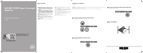
戴尔易安信XC640 超融合一体机入门指南说明书
技术规格
以下仅是依照法律规定随您的设备附带的规格。有关您的设备规格的当前完整列表,请访问 /XCSeriesmanuals。
电源: 2000 W 铂金 AC 100–240 V,50/60 Hz,11.5 A
注:如果设备使用低压线路 100-120 V AC 运行,则每个 PSU 的额定功率会降至 1000 W。 1600 W 铂金 AC 200–240 V,50/60 Hz,10 A
Before using your appliance, read the Dell Software License Agreement that is shipped with your appliance. If you do not accept the terms of agreement, see /contactdell.
注:适用于您的设备的说明文件集可从 /XCSeriesmanuals 上获取。确保始终针对所有最新更新确认此文档集。 注:确保在安装未随设备一起购买的硬件或软件之前安装操作系 统。有关支持的操作系统的详细信息,请访问 /ossupport。 注:PSU 输入连接器可能因 PSU 类型而异。
Power: 2000 W Platinum AC 100–240 V, 50/60 Hz, 11.5 A
NOTE: If appliance operates at low line 100–120 V AC, then the power rating per PSU is derated to 1000 W. 1600 W Platinum AC 200–240 V, 50/60 Hz, 10 A
- 1、下载文档前请自行甄别文档内容的完整性,平台不提供额外的编辑、内容补充、找答案等附加服务。
- 2、"仅部分预览"的文档,不可在线预览部分如存在完整性等问题,可反馈申请退款(可完整预览的文档不适用该条件!)。
- 3、如文档侵犯您的权益,请联系客服反馈,我们会尽快为您处理(人工客服工作时间:9:00-18:30)。
GS864018/32/36T-300/250/200/1674M x 18, 2M x 32, 2M x 3672Mb Sync Burst SRAMs 300 MHz –167 MHz 2.5 V or 3.3 V V DD 2.5 V or 3.3 V I/O100-Pin TQFP Commercial Temp Industrial Temp Features• FT pin for user-configurable flow through or pipeline operation• Single Cycle Deselect (SCD) operation• 2.5 V or 3.3 V +10%/–10% core power supply • 2.5 V or 3.3 V I/O supply• LBO pin for Linear or Interleaved Burst mode• Internal input resistors on mode pins allow floating mode pins • Default to Interleaved Pipeline mode• Byte Write (BW) and/or Global Write (GW) operation • Internal self-timed write cycle• Automatic power-down for portable applications • JEDEC-standard 100-lead TQFP package • Pb-Free 100-lead TQFP package availableFunctional DescriptionApplicationsThe GS864018/32/36T is a 75,497,472-bit high performance synchronous SRAM with a 2-bit burst address counter. Although of a type originally developed for Level 2 Cache applications supporting high performance CPUs, the device now finds application in synchronous SRAM applications, ranging from DSP main store to networking chip set support. ControlsAddresses, data I/Os, chip enables (E1, E2, E3), address burst control inputs (ADSP, ADSC, ADV), and write control inputs (Bx, BW, GW) are synchronous and are controlled by a positive-edge-triggered clock input (CK). Output enable (G) and power down control (ZZ) are asynchronous inputs. Burstcycles can be initiated with either ADSP or ADSC inputs. In Burst mode, subsequent burst addresses are generated internally and are controlled by ADV. The burst address counter may be configured to count in either linear orinterleave order with the Linear Burst Order (LBO) input. The Burst function need not be used. New addresses can be loaded on every cycle with no degradation of chip performance.Flow Through/Pipeline ReadsThe function of the Data Output register can be controlled by the user via the FT mode pin (Pin 14). Holding the FT mode pin low places the RAM in Flow Through mode, causing output data to bypass the Data Output Register. Holding FT high places the RAM in Pipeline mode, activating the rising-edge-triggered Data Output Register.Byte Write and Global WriteByte write operation is performed by using Byte Write enable (BW) input combined with one or more individual byte write signals (Bx). In addition, Global Write (GW) is available for writing all bytes at one time, regardless of the Byte Write control inputs.Sleep ModeLow power (Sleep mode) is attained through the assertion (High) of the ZZ signal, or by stopping the clock (CK). Memory data is retained during Sleep mode.Core and Interface VoltagesThe GS864018/32/36T operates on a 2.5 V or 3.3 V power supply. All input are 3.3 V and 2.5 V compatible. Separate output power (V DDQ ) pins are used to decouple output noise from the internal circuits and are 3.3 V and 2.5 V compatible.Parameter Synopsis-300-250-200-167Unit Pipeline 3-1-1-1KQ tCycle 3.3 4.0 5.0 6.0ns (x18)Curr (x32/x36)480410350305mA Flow Through 2-1-1-1t KQ tCycle 5.55.5 6.56.57.57.58.08.0ns ns Curr (x18)Curr (x32/x36)285330245280220250210240mA mA807978777675747372717069686766656463626160595857565554535251123456789101112131415161718192021222324252627282930V DDQ V SS DQ B DQ B V SS V DDQ DQ B DQ B V DD NC V SS DQ B DQ B V DDQ V SS DQ B DQ B DQP BV SS V DDQ V DDQ V SS DQ A DQ A V SS V DDQ DQ A DQ A V SS NC V DD ZZ DQ A DQ A V DDQ V SS DQ A DQ A V SS V DDQ L B O A A A A A 1A 0A A V S SV D DA A A A A A A AA A E 1E 2 N C N C B BB AE 3C K G W B W VD DV S SG A D S C A D S P A D V A AA 4M x 18Top View DQP A A NC NC NC NC NC NC NC NCNC NC NC NC NC NC NCNC NC 100999897969594939291908988878685848382813132333435363738394041424344454647484950FT GS864018/32/36T-300/250/200/167GS864018 100-Pin TQFP Pinout (Package T)807978777675747372717069686766656463626160595857565554535251123456789101112131415161718192021222324252627282930V DDQ V SS DQ C DQ C V SS V DDQ DQ C DQ C V DD NC V SS DQ D DQ D V DDQ V SS DQ D DQ D DQ D V SS V DDQ V DDQ V SS DQ B DQ B V SS V DDQ DQ B DQ B V SS NC V DD ZZ DQ A DQ A V DDQ V SS DQ A DQ A V SS V DDQ L B O A A A A A 1A 0A A V S SV D DA A A A A A A AA A E 1E 2 B DB CB BB AE 3C K G W B W VD DV S SG A D S C A D S P A D V A AA 2M x 32Top View DQB NC DQ B DQ B DQ B DQ A DQ A DQ A DQ A NCDQ C DQ C DQ C DQ D DQ D DQ D NCDQ C NC 100999897969594939291908988878685848382813132333435363738394041424344454647484950FT GS864018/32/36T-300/250/200/167GS864032 100-Pin TQFP Pinout (Package T)807978777675747372717069686766656463626160595857565554535251123456789101112131415161718192021222324252627282930V DDQ V SS DQ C DQ C3V SS V DDQ DQ C DQ C V DD NC V SS DQ D DQ D V DDQ V SS DQ D DQ D DQ D V SS V DDQ V DDQ V SS DQ B DQ B V SS V DDQ DQ B DQ B V SS NC V DD ZZ DQ A DQ A V DDQ V SS DQ A DQ A V SS V DDQ L B O A A A A A 1A 0A A V S SV D DA A A A A A A AA A E 1E 2 B DB CB BB AE 3C K G W B W VD DV S SG A D S C A D S P A D V A AA 2M x 36Top View DQB DQP B DQ B DQ B DQ B DQ A DQ A DQ A DQ A DQP ADQ C DQ C DQ C DQ D DQ D DQ D DQP DDQ C DQP C 100999897969594939291908988878685848382813132333435363738394041424344454647484950FT GS864018/32/36T-300/250/200/167GS864036 100-Pin TQFP Pinout (Package T)TQFP Pin DescriptionSymbolTypeDescriptionA 0, A 1I Address field LSBs and Address Counter preset InputsA I Address Inputs DQ A DQB DQC DQD I/OData Input and Output pinsNC No ConnectBW I Byte Write —Writes all enabled bytes; active low B A , B B I Byte Write Enable for DQ A , DQ B Data I/Os; active low B C , B D I Byte Write Enable for DQ C , DQ D Data I/Os; active lowCK I Clock Input Signal; active highGW I Global Write Enable —Writes all bytes; active lowE 1, E 3I Chip Enable; active low E 2I Chip Enable; active high G I Output Enable; active lowADV I Burst address counter advance enable; active low ADSP, ADSCI Address Strobe (Processor, Cache Controller); active lowZZ I Sleep Mode control; active high FT I Flow Through or Pipeline mode; active low LBO I Linear Burst Order mode; active lowV DD I Core power supply V SS I I/O and Core Ground V DDQIOutput driver power supplyGS864018/32/36T-300/250/200/167GS864018/32/36T-300/250/200/167A1A0A0A1D0D1Q1Q0Counter LoadD QDQRegisterRegisterDQRegisterDQRegisterDQRegisterD QRegisterD QRegisterD QRegisterDQR e g i s t e rDQRegisterA0–AnLBO ADV CK ADSC ADSP GW BW E 1GZZPower Down ControlMemory Array36364AQDE 2E 3DQx1–DQx9Note: Only x36 version shown for simplicity.B AB BB CB DFT GS864018/32/36 Block DiagramMode Pin FunctionsMode NamePin NameStateFunctionBurst Order Control LBO L Linear Burst H Interleaved Burst Output Register Control FT L Flow Through H or NC Pipeline Power Down Control ZZ L or NC Active H Standby, I DD = I SB Single/Dual Cycle Deselect Control SCD L Dual Cycle Deselect H or NC Single Cycle Deselect FLXDrive Output Impedance ControlZQ L High Drive (Low Impedance)H or NC Low Drive (High Impedance)9th Bit EnablePEL or NC Activate DQPx I/Os (x18/x3672 mode)HDeactivate DQPx I/Os (x16/x3272 mode)GS864018/32/36T-300/250/200/167Note:There is a are pull-up devices on the ZQ, SCD, and FT pins and a pull-down device on the ZZ pin, so thosethis input pins can be unconnected and the chip will operate in the default states as specified in the above tables.Note:The burst counter wraps to initial state on the 5th clock.Note:The burst counter wraps to initial state on the 5th clock.Linear Burst SequenceA[1:0]A[1:0]A[1:0]A[1:0]1st address 000110112nd address 011011003rd address 101100014th address11000110Interleaved Burst SequenceA[1:0]A[1:0]A[1:0]A[1:0]1st address 000110112nd address 010011103rd address 101100014th address11100100Burst Counter SequencesBPR 1999.05.18GS864018/32/36T-300/250/200/167Byte Write Truth TableFunctionGWBWB AB BB CB DNotesRead H H X X X X 1Read H L H H H H 1Write byte a H L L H H H 2, 3Write byte b H L H L H H 2, 3Write byte c H L H H L H 2, 3, 4Write byte d H L H H H L 2, 3, 4Write all bytesHLLLLL2, 3, 4Write all bytes L X X X X X1.All byte outputs are active in read cycles regardless of the state of Byte Write Enable inputs.2.Byte Write Enable inputs B A , B B , B C and/or B D may be used in any combination with BW to write single or multiple bytes.3.All byte I/Os remain High-Z during all write operations regardless of the state of Byte Write Enable inputs.4.Bytes “C ” and “D ” are only available on the x32 and x36 versions.Synchronous Truth TableOperationAddress UsedState Diagram Key 5E 1E 2ADSP ADSCADVW 3DQ 4Deselect Cycle, Power Down None X H X X L X X High-Z Deselect Cycle, Power Down None X L F L X X X High-Z Deselect Cycle, Power Down None X L F H L X X High-Z Read Cycle, Begin Burst External R L T L X X X Q Read Cycle, Begin Burst External R L T H L X F Q Write Cycle, Begin Burst External W L T H L X T D Read Cycle, Continue Burst Next CR X X H H L F Q Read Cycle, Continue Burst Next CR H X X H L F Q Write Cycle, Continue Burst Next CW X X H H L T D Write Cycle, Continue Burst Next CWH X X H L T D Read Cycle, Suspend Burst Current X X H H H F Q Read Cycle, Suspend Burst Current H X X H H F Q Write Cycle, Suspend BurstCurrentXXHHHTDWrite Cycle, Suspend Burst Current H X X H H T D 1.X = Don’t Care, H = High, L = Low2. E = T (True) if E 2 = 1 and E 3 = 0; E = F (False) if E 2 = 0 or E 3 = 13.W = T (True) and F (False) is defined in the Byte Write Truth Table preceding.4.G is an asynchronous input. G can be driven high at any time to disable active output drivers. G low can only enable active drivers (shownas “Q” in the Truth Table above).5.All input combinations shown above are tested and supported. Input combinations shown in gray boxes need not be used to accomplishbasic synchronous or synchronous burst operations and may be avoided for simplicity.6.Tying ADSP high and ADSC low allows simple non-burst synchronous operations. See BOLD items above.7.Tying ADSP high and ADV low while using ADSC to load new addresses allows simple burst operations. See ITALIC items above.GS864018/32/36T-300/250/200/167First WriteFirst ReadBurst WriteBurst ReadDeselect R WCRCWXXWRRWRXXX S i m p l e S y n c h r o n o u s O p e r a t i o nS i m p l e B u r s t S y n c h r o n o u s O p e r a t i o nCR RCWCRCRNotes:1.The diagram shows only supported (tested) synchronous state transitions. The diagram presumes G is tied low.2.The upper portion of the diagram assumes active use of only the Enable (E1) and Write (B A , B B , B C , B D , BW, and GW) control inputs, andthat ADSP is tied high and ADSC is tied low.3.The upper and lower portions of the diagram together assume active use of only the Enable, Write, and ADSC control inputs, andassumes ADSP is tied high and ADV is tied low.GS864018/32/36T-300/250/200/167Simplified State DiagramFirst WriteFirst ReadBurst WriteBurst ReadDeselectR WCRCWXXWRRWRXXX CRR CW CRCRW CWW CWNotes:1.The diagram shows supported (tested) synchronous state transitions plus supported transitions that depend upon the use of G.e of “Dummy Reads” (Read Cycles with G High) may be used to make the transition from Read cycles to Write cycles without passingthrough a Deselect cycle. Dummy Read cycles increment the address counter just like normal read cycles.3.Transitions shown in gray tone assume G has been pulsed high long enough to turn the RAM’s drivers off and for incoming data to meetData Input Set Up Time.GS864018/32/36T-300/250/200/167Simplified State Diagram with GGS864018/32/36T-300/250/200/167Absolute Maximum Ratings(All voltages reference to V SS )SymbolDescriptionValueUnitV DD Voltage on V DD Pins –0.5 to 4.6V V DDQ Voltage in V DDQ Pins –0.5 to 4.6V V I/O Voltage on I/O Pins –0.5 to V DDQ +0.5 (≤ 4.6 V max.)V V IN Voltage on Other Input Pins –0.5 to V DD +0.5 (≤ 4.6 V max.)V I IN Input Current on Any Pin +/–20mA I OUT Output Current on Any I/O Pin +/–20mA P D Package Power Dissipation 1.5WT STG Storage Temperature –55 to 125o C T BIASTemperature Under Bias–55 to 125oCNote:Permanent damage to the device may occur if the Absolute Maximum Ratings are exceeded. Operation should be restricted to Recommended Operating Conditions. Exposure to conditions exceeding the Absolute Maximum Ratings, for an extended period of time, may affect reliability of this component. Power Supply Voltage RangesParameterSymbolMin.Typ.Max.UnitNotes3.3 V Supply Voltage V DD3 3.0 3.3 3.6V 2.5 V Supply Voltage V DD2 2.3 2.5 2.7V 3.3 V V DDQ I/O Supply Voltage V DDQ3 3.0 3.3 3.6V 2.5 V V DDQ I/O Supply VoltageV DDQ22.32.52.7VNotes:1.The part numbers of Industrial Temperature Range versions end the character “I”. Unless otherwise noted, all performance specifica-tions quoted are evaluated for worst case in the temperature range marked on the device.2.Input Under/overshoot voltage must be –2 V > Vi < V DDn +2 V not to exceed 4.6 V maximum, with a pulse width not to exceed 20% tKC.GS864018/32/36T-300/250/200/167V DDQ3 Range Logic LevelsParameterSymbolMin.Typ.Max.UnitNotesV DD Input High Voltage V IH 2.0—V DD + 0.3V 1V DD Input Low Voltage V IL –0.3—0.8V 1V DDQ I/O Input High Voltage V IHQ 2.0—V DDQ + 0.3V 1,3V DDQ I/O Input Low VoltageV ILQ–0.3—0.8V1,3Notes:1.The part numbers of Industrial Temperature Range versions end the character “I”. Unless otherwise noted, all performance specifica-tions quoted are evaluated for worst case in the temperature range marked on the device.2.Input Under/overshoot voltage must be –2 V > Vi < V DDn +2 V not to exceed 4.6 V maximum, with a pulse width not to exceed 20% tKC.3.V IHQ (max) is voltage on V DDQ pins plus 0.3 V.V DDQ2 Range Logic LevelsParameterSymbolMin.Typ.Max.UnitNotesV DD Input High Voltage V IH 0.6*V DD —V DD + 0.3V 1V DD Input Low Voltage V IL –0.3—0.3*V DD V 1V DDQ I/O Input High Voltage V IHQ 0.6*V DD —V DDQ + 0.3V 1,3V DDQ I/O Input Low VoltageV ILQ–0.3—0.3*V DDV1,3Notes:1.The part numbers of Industrial Temperature Range versions end the character “I”. Unless otherwise noted, all performance specifica-tions quoted are evaluated for worst case in the temperature range marked on the device.2.Input Under/overshoot voltage must be –2 V > Vi < V DDn +2 V not to exceed 4.6 V maximum, with a pulse width not to exceed 20% tKC.3.V IHQ (max) is voltage on V DDQ pins plus 0.3 V.Recommended Operating TemperaturesParameterSymbolMin.Typ.Max.UnitNotesAmbient Temperature (Commercial Range Versions)T A 02570°C 2Ambient Temperature (Industrial Range Versions)T A–402585°C2Notes:1.The part numbers of Industrial Temperature Range versions end the character “I”. Unless otherwise noted, all performance specifica-tions quoted are evaluated for worst case in the temperature range marked on the device.2.Input Under/overshoot voltage must be –2 V > Vi < V DDn +2 V not to exceed 4.6 V maximum, with a pulse width not to exceed 20% tKC.GS864018/32/36T-300/250/200/16720% tKCV SS – 2.0 V50%V SS V IHUndershoot Measurement and TimingOvershoot Measurement and Timing20% tKCV DD + 2.0 V50%V DDV ILCapacitanceo C, f = 1 MH Z , V DD ParameterSymbolTest conditionsTyp.Max.UnitInput Capacitance C IN V IN = 0 V 45pF Input/Output Capacitance C I/OV OUT = 0 V67pFNote:These parameters are sample tested.AC Test ConditionsParameterConditionsInput high level V DD – 0.2 V Input low level 0.2 V Input slew rate 1 V/ns Input reference level V DDQ /2Output reference levelV DDQ /2Output loadFig. 1Notes:1.Include scope and jig capacitance.2.Test conditions as specified with output loading as shown in Fig. 1unless otherwise noted.3.Device is deselected as defined by the Truth Table.DQV DDQ/250Ω30pF *Output Load 1* Distributed Test Jig Capacitance(T A = 25= 2.5 V)DC Electrical CharacteristicsParameterSymbolTest ConditionsMinMaxInput Leakage Current (except mode pins)I IL V IN = 0 to V DD –2 uA 2 uA ZZInput Current I IN1V DD ≥ V IN ≥ V IH 0 V ≤ V IN ≤ V IH –1 uA –1 uA 1 uA 100 uA FTInput CurrentI IN2V DD ≥ V IN ≥ V IL 0 V ≤ V IN ≤ V IL–100 uA –1 uA 1 uA 1 uA Output Leakage Current (x36/x72)I OL Output Disable, V OUT = 0 to V DD –1 uA 1 uA Output Leakage Current (x18)I OL Output Disable, V OUT = 0 to V DD –1 uA 1 uA Output High Voltage V OH2I OH = –8 mA, V DDQ = 2.375 V 1.7 V —Output High Voltage V OH3I OH = –8 mA, V DDQ = 3.135 V2.4 V —Output Low VoltageV OLI OL = 8 mA—0.4 VGS864018/32/36T-300/250/200/167Operating CurrentsParameterTest ConditionsModeSymbol-300-250-200-167Unit0to 70°C –40 to 85°C 0to 70°C –40 to 85°C 0to 70°C –40to 85°C 0 to 70°C –40to 85°C Operating CurrentDevice Selected; All other inputs ≥V IH o r ≤ V IL Output open(x32/x36)Pipeline I DD I DDQ 4206044060360503805031040330402703529035mA Flow Through I DD I DDQ 3003032030255252752523020250202202024020mA (x18)PipelineI DD I DDQ 3703039030315253352527020290202402026020mA Flow Through I DD I DDQ 2701529015230152501520515225151951521515mA Standby Current ZZ ≥ V DD – 0.2 V —PipelineI SB 100120100120100120100120mA Flow Through I SB 100120100120100120100120mA Deselect CurrentDevice Deselected; All other inputs ≥ V IH or ≤ V IL—Pipeline I DD 150165140155130146125140mA Flow ThroughI DD135150125140120135120135mAGS864018/32/36T-300/250/200/167Notes:1.I DD and I DDQ apply to any combination of V DD3, V DD2, V DDQ3, and V DDQ2 operation.2.All parameters listed are worst case scenario.AC Electrical CharacteristicsParameter Symbol -300-250-200-167Unit Min Max MinMax MinMax MinMax PipelineClock Cycle Time tKC 3.3— 4.0— 5.0— 6.0—ns Clock to Output ValidtKQ — 2.3— 2.5— 3.0— 3.5ns Clock to Output Invalid tKQX 1.5— 1.5— 1.5— 1.5—ns Clock to Output in Low-ZtLZ 1 1.5— 1.5— 1.5— 1.5—ns Setup time tS 1.1— 1.2— 1.4— 1.5—ns Hold time tH 0.1—0.2—0.4—0.5—ns Flow ThroughClock Cycle Time tKC 5.5— 6.5—7.5—8.0—ns Clock to Output ValidtKQ — 5.5— 6.5—7.5—8.0ns Clock to Output Invalid tKQX 3.0— 3.0— 3.0— 3.0—ns Clock to Output in Low-ZtLZ 1 3.0— 3.0— 3.0— 3.0—ns Setup time tS 1.5— 1.5— 1.5— 1.5—ns Hold time tH 0.5—0.5—0.5—0.5—ns Clock HIGH Time tKH 1.0— 1.3— 1.3— 1.3—ns Clock LOW Time tKL 1.2— 1.5— 1.5— 1.5—ns Clock to Output inHigh-Z tHZ 1 1.5 2.3 1.5 2.5 1.5 3.0 1.5 3.0ns G to Output Valid tOE — 2.3— 2.5— 3.0— 3.5ns G to output in Low-Z tOLZ 10—0—0—0—ns G to output in High-Z tOHZ 1— 2.3— 2.5— 3.0— 3.0ns ZZ setup time tZZS 25—5—5—5—ns ZZ hold time tZZH 21—1—1—1—ns ZZ recoverytZZR20—20—20—20—nsGS864018/32/36T-300/250/200/167Notes:1.These parameters are sampled and are not 100% tested.2.ZZ is an asynchronous signal. However, in order to be recognized on any given clock cycle, ZZ must meet the specified setup and holdtimes as specified above.GS864018/32/36T-300/250/200/167Pipeline Mode Timing (SCD)Begin Read A Cont Cont Deselect Write B Read C Read C+1Read C+2Read C+3ContDeselecttHZtKQX tKQtLZtHtStOHZtOEtHtStHtStHtStHtStHtStStHtStHtStHtSBurst ReadtKCtKL tKH Single Write Single ReadQ(A)D(B)Q(C)Q(C+1)Q(C+2)Q(C+3)ABCDeselected with E1E1 masks ADSPE2 and E3 only sampled with ADSP and ADSCADSC initiated readCK ADSPADSCADVA0–AnGWBWBa–BdE1E2E3GDQa–DQdGS864018/32/36T-300/250/200/167Flow Through Mode Timing (SCD)Begin Read A ContCont Write B Read C Read C+1Read C+2Read C+3Read C Cont DeselecttHZtKQXtKQ tLZtH tStOHZtOEtHtS tHtS tHtStHtS tHtS tHtStHtS tHtS tH tS tHtS tKCtKL tKHABCQ(A)D(B)Q(C)Q(C+1)Q(C+2)Q(C+3)Q(C)E2 and E3 only sampled with ADSCADSC initiated readDeselected with E1Fixed HighCK ADSPADSCADVA0–AnGWBWBa–BdE1E2E3GDQa–DQdGS864018/32/36T-300/250/200/167Sleep ModeDuring normal operation, ZZ must be pulled low, either by the user or by its internal pull down resistor. When ZZ is pulled high, the SRAM will enter a Power Sleep mode after 2 cycles. At this time, internal state of the SRAM is preserved. When ZZ returns to low, the SRAM operates normally after 2 cycles of wake up time.Sleep mode is a low current, power-down mode in which the device is deselected and current is reduced to I SB 2. The duration of Sleep mode is dictated by the length of time the ZZ is in a High state. After entering Sleep mode, all inputs except ZZ become disabled and all outputs go to High-Z The ZZ pin is an asynchronous, active high input that causes the device to enter Sleep mode. When the ZZ pin is driven high, I SB 2 is guaranteed after the time tZZI is met. Because ZZ is an asynchronous input, pending operations or operations in progress may not be properly completed if ZZ is asserted. Therefore, Sleep mode must not be initiated until valid pending operations are completed. Similarly, when exiting Sleep mode during tZZR, only a Deselect or Read commands may be applied while the SRAM is recovering from Sleep mode.Sleep Mode Timing DiagramtZZRtZZHtZZSHoldSetup tKLtKHtKCCKADSP ADSCZZGS864018/32/36T-300/250/200/167TQFP Package Drawing (Package T) D1D E1EPin 1be cLL1A2A1YθNotes:1.All dimensions are in millimeters (mm).2.Package width and length do not include mold protrusion.SymbolDescriptionMin.Nom.MaxA1Standoff 0.050.100.15A2Body Thickness 1.35 1.40 1.45b Lead Width 0.200.300.40c Lead Thickness 0.09—0.20D Terminal Dimension 21.922.022.1D1Package Body 19.920.020.1E Terminal Dimension 15.916.016.1E1Package Body 13.914.014.1e Lead Pitch —0.65—L Foot Length 0.450.600.75L1Lead Length —1.00—Y Coplanarity 0.10θLead Angle0°—7°GS864018/32/36T-300/250/200/167Ordering Information for GSI Synchronous Burst RAMs OrgPart Number1TypePackageSpeed 2(MHz/ns)T A 3Status4M x 18GS864018T-300Pipeline/Flow Through TQFP 300/5.5C 4M x 18GS864018T-250Pipeline/Flow Through TQFP 250/6.5C 4M x 18GS864018T-200Pipeline/Flow Through TQFP 200/7.5C 4M x 18GS864018T-167Pipeline/Flow Through TQFP 167/8C 2M x 32GS864032T-300Pipeline/Flow Through TQFP 300/5.5C 2M x 32GS864032T-250Pipeline/Flow Through TQFP 250/6.5C 2M x 32GS864032T-200Pipeline/Flow Through TQFP 200/7.5C 2M x 32GS864032T-167Pipeline/Flow Through TQFP 167/8C 2M x 36GS864036T-300Pipeline/Flow Through TQFP 300/5.5C 2M x 36GS864036T-250Pipeline/Flow Through TQFP 250/6.5C 2M x 36GS864036T-200Pipeline/Flow Through TQFP 200/7.5C 2M x 36GS864036T-167Pipeline/Flow Through TQFP 167/8C 4M x 18GS864018T-300I Pipeline/Flow Through TQFP 300/5.5I 4M x 18GS864018T-250I Pipeline/Flow Through TQFP 250/6.5I 4M x 18GS864018T-200I Pipeline/Flow Through TQFP 200/7.5I 4M x 18GS864018T-167I Pipeline/Flow Through TQFP 167/8I 2M x 32GS864032T-300I Pipeline/Flow Through TQFP 300/5.5I 2M x 32GS864032T-250I Pipeline/Flow Through TQFP 250/6.5I 2M x 32GS864032T-200I Pipeline/Flow Through TQFP 200/7.5I 2M x 32GS864032T-167I Pipeline/Flow Through TQFP 167/8I 2M x 36GS864036T-300I Pipeline/Flow Through TQFP 300/5.5I 2M x 36GS864036T-250I Pipeline/Flow Through TQFP 250/6.5I 2M x 36GS864036T-200I Pipeline/Flow Through TQFP 200/7.5I 2M x 36GS864036T-167I Pipeline/Flow Through TQFP 167/8I 4M x 18GS864018GT-250Pipeline/Flow Through Pb-Free TQFP 250/6.5C 4M x 18GS864018GT-200Pipeline/Flow Through Pb-Free TQFP 200/7.5C 4M x 18GS864018GT-167Pipeline/Flow Through Pb-Free TQFP 167/8C 2M x 32GS864032GT-300Pipeline/Flow ThroughPb-Free TQFP300/5.5C2M x 32GS864032GT-250Pipeline/Flow Through Pb-Free TQFP 250/6.5C Notes:1.Customers requiring delivery in Tape and Reel should add the character “T” to the end of the part number. Example: GS864018T-300IT.2.The speed column indicates the cycle frequency (MHz) of the device in Pipeline mode and the latency (ns) in Flow Through mode. Eachdevice is Pipeline/Flow Through mode-selectable by the user.3.T A = C = Commercial Temperature Range. T A = I = Industrial Temperature Range.4. GSI offers other versions this type of device in many different configurations and with a variety of different features, only some of which arecovered in this data sheet. See the GSI Technology web site () for a complete listing of current offerings.GS864018/32/36T-300/250/200/1672M x 32GS864032GT-200Pipeline/Flow Through Pb-Free TQFP 200/7.5C 2M x 32GS864032GT-167Pipeline/Flow Through Pb-Free TQFP 167/8C 2M x 36GS864036GT-250Pipeline/Flow Through Pb-Free TQFP 250/6.5C 2M x 36GS864036GT-200Pipeline/Flow Through Pb-Free TQFP 200/7.5C 2M x 36GS864036GT-167Pipeline/Flow Through Pb-Free TQFP 167/8C 4M x 18GS864018GT-300I Pipeline/Flow Through Pb-Free TQFP 300/5.5I 4M x 18GS864018GT-250I Pipeline/Flow Through Pb-Free TQFP 250/6.5I 4M x 18GS864018GT-200I Pipeline/Flow Through Pb-Free TQFP 200/7.5I 4M x 18GS864018GT-167I Pipeline/Flow Through Pb-Free TQFP 167/8I 2M x 32GS864032GT-300I Pipeline/Flow Through Pb-Free TQFP 300/5.5I 2M x 32GS864032GT-250I Pipeline/Flow Through Pb-Free TQFP 250/6.5I 2M x 32GS864032GT-200I Pipeline/Flow Through Pb-Free TQFP 200/7.5I 2M x 32GS864032GT-167I Pipeline/Flow Through Pb-Free TQFP 167/8I 2M x 36GS864036GT-300I Pipeline/Flow Through Pb-Free TQFP 300/5.5I 2M x 36GS864036GT-250I Pipeline/Flow Through Pb-Free TQFP 250/6.5I 2M x 36GS864036GT-200IPipeline/Flow ThroughPb-Free TQFP200/7.5I2M x 36GS864036GT-167I Pipeline/Flow Through Pb-Free TQFP 167/8I Ordering Information for GSI Synchronous Burst RAMs (Continued)OrgPart Number1TypePackageSpeed 2(MHz/ns)T A 3StatusNotes:1.Customers requiring delivery in Tape and Reel should add the character “T” to the end of the part number. Example: GS864018T-300IT.2.The speed column indicates the cycle frequency (MHz) of the device in Pipeline mode and the latency (ns) in Flow Through mode. Eachdevice is Pipeline/Flow Through mode-selectable by the user.3.T A = C = Commercial Temperature Range. T A = I = Industrial Temperature Range.4. GSI offers other versions this type of device in many different configurations and with a variety of different features, only some of which arecovered in this data sheet. See the GSI Technology web site () for a complete listing of current offerings.。