SZ2575中文资料
ZST-136-04-F-D-0735中文资料(SAMTEC)中文数据手册「EasyDatasheet - 矽搜」

指定
LEAD STYLE from 图.
(2,54) .100
(2,54) .100
(0,64) .025 SQ TYP
(2,29) .090 MIN
(2,54) .100
–F
= Gold flash on post, Matte Tin on tail
–“XXXX”
= Body Height
–L
= 10µ" (0,25 µm) Gold on post,
应用 特定选项
•定位销 •单列 •锁定信息 •极化 请致电Samtec公司.
Note: Other Gold plating options available. Contact Samtec. Note: Some lengths, styles and optionsare non-standard, non-returnable. ZST is non-standard, non-returnable.
–L
= 10µ" (0,25 µm) Gold on post, Matte Tin on tail
–T
= Matte Tin
LEAD ANGRLIGEHT
STYLE (B)
–04 (3,30) .130
–05 (5,84) .230
B
–D
= Double Row Through-hole (lead style –01, –02 & –03 only)
芯片中文手册,看全文,戳
F-213-1
ZST–113–03–L–D–0735
(2,54 mm) .100" TST,HTST,ZST系列
HTST–125–01–L–DV
LM2575HV中文资料(上)
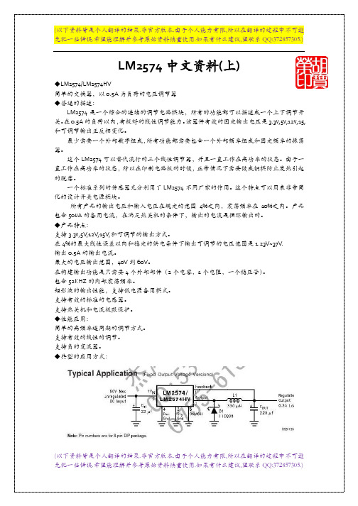
(以下资料皆是个人翻译的结果.非官方版本.由于个人能力有限,所以在翻译的过程中不可避 免犯一些错误.希望能理解并参考原始资料慎重使用.如果有什么建议,望联系 QQ:372857305.)LM2574 中文资料(上)◆LM2574/LM2574HV 简单的交换器,以 0.5A 为负荷的电压调节器 ◆普通的描述: LM2574 是一个综合的连续的调节电路模块,所有的功能都可以描述成一个上下调节开 关。
0.5A 的负荷以内, 在 有极好的线性调节能力。
该器件有效的固定输出电压是 3.3v,5v,12v,15, 和可调节输出正反相变化。
最少需要一个外部数字组成, 所有功能都需要包含一个外部频率组成和固定频率的振荡 器。
这个 LM2574 可以替代流行的三个线性调节器,并且一直工作在高功率的状态。
由于一 直工作在高功率的状态, 所以在印制电路板的时候, 正常情况下需要做成铜模防止发热引起 的脱落。
一个标准系列的传感器充分利用了 LM2574 不同厂家的作用。
这个特点可以用来非常简 化的设计开关电源模块。
所有产品的输出电压和输入电压在规定的范围 4%之内,震荡频率在 10%之内。
产品 包含 50uA 的备用电流,在满足热关机的条件下,输出的电流是循环输出的。
◆产品特点: 支持 3.3v,5V,12V,15V,和可调节的输出方式。
在 4%的最大线性误差以内和稳定的供电条件下输出可调节的电压范围是 1.23V~37V. 输出 0.5A 的输出电流。
最大的电压输出范围,40V 到 60V。
在构建输出功能是只需要 4 个外部部件(2 个电容,1 个电阻,一个稳压管) 。
包含 52KHZ 的内部震荡频率。
矩形波的输出性能,支持低电源备用模式。
支持有效的标准的电感器。
支持热关机和电流极限保护。
◆性能应用: 简单的高频率逐周期的调节方式。
支持有效的线性的调节。
支持负的变流器。
◆典型的应用方式:(以下资料皆是个人翻译的结果.非官方版本.由于个人能力有限,所以在翻译的过程中不可避 免犯一些错误.希望能理解并参考原始资料慎重使用.如果有什么建议,望联系 QQ:372857305.)(以下资料皆是个人翻译的结果.非官方版本.由于个人能力有限,所以在翻译的过程中不可避 免犯一些错误.希望能理解并参考原始资料慎重使用.如果有什么建议,望联系 QQ:372857305.)60V 未校准的 DC 输入◆连接图解:校准的 0.5A 输出◆极限参数: 如果用在军队或者航天上面,则必须用详细的(更好的)设备。
LM2575(开关稳压管)中文资料

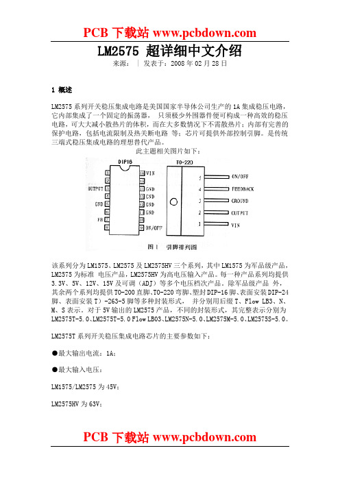
LM2575 超详细中文介绍1 概述LM2575系列开关稳压集成电路是美国国家半导体公司生产的1A集成稳压电路,它内部集成了一个固定的振荡器,只须极少外围器件便可构成一种高效的稳压电路,可大大减小散热片的体积,而在大多数情况下不需散热片;内部有完善的保护电路,包括电流限制及热关断电路等;芯片可提供外部控制引脚。
是传统三端式稳压集成电路的理想替代产品。
此主题相关图片如下:该系列分为LM1575、LM2575及LM2575HV三个系列,其中LM1575为军品级产品,LM2575为标准电压产品,LM2575HV为高电压输入产品。
每一种产品系列均提供3.3V、5V、12V、15V及可调(ADJ)等多个电压档次产品。
除军品级产品外,其余两个系列均提供TO-200直脚、TO-220弯脚、塑封DIP-16脚、表面安装DIP-24脚、表面安装T)-263-5脚等多种封装形式,并分别用后缀T、Flow LB3、N、M、S表示。
对于5V输出的LM2575产品,不同的封装形式,其完整表示分别为LM2575T-5.0、LM2575T-5.0 Flow LB03、LM2575N-5.0、LM2575M-5.0、LM2575S-5.0。
LM2575T系列开关稳压集成电路芯片的主要参数如下:●最大输出电流:1A;●最大输入电压:LM1575/LM2575为45V;LM2575HV为63V;●输出电压:3.3V、5V、12V、ADJ(可调);●振荡频率:54kHz;●最大稳压误差:4%;●转换效率:75%~88%(不同的电压输出的效率不同);●工作温度范围:LM1575为-55℃~+150℃;LM2575/LM2575HV为-40℃~+125℃。
2 引脚功能图1是LM2575集成稳压器的两种引脚排列。
其引脚功能如下:VIN:未稳压电压输入端;OUTPUT:开关电压输出,接电感及快恢复二极管;GND:公共端;FEEDBACK:反馈输入端;ON/OFF:控制输入端,接公共端时,稳压电路工作;接高电平时,稳压电路停止。
TL2575_0701中文资料

FEATURESAPPLICATIONSNCNCOUTPUTNCGNDNCFEEDBACKNCN (PDIP) PACKAGE(TOP VIEW)KTT (TO-263) PACKAGE(TOP VIEW)12345GNDON/OFFFEEDBACKGNDOUTPUTV INFEEDBACKKV (TO-220 STAGGERED LEADS) PACKAGE(TOP VIEW)(SIDE VIEW)Pins 1, 3, 5Pins 2, 4 DESCRIPTION/ORDERING INFORMATION1-A SIMPLE STEP-DOWN SWITCHING VOLTAGE REGULATORSSLVS638B–MAY2006–REVISED JANUARY2007•Fixed3.3-V,5-V,12-V,and15-V Options With±5%Regulation(Max)Over Line,Load,andTemperature Conditions•Adjustable Option With a Range of1.23V to37V(57V for HV Version)and±4%Regulation(Max)Over Line,Load,andTemperature Conditions•Specified1-A Output Current•Wide Input Voltage Range…4.75V to40V(60V for HV Version)•Require Only Four External Components(Fixed Versions)and Use Readily AvailableStandard Inductors•52-kHz(Typ)Fixed-Frequency InternalOscillator•TTL Shutdown Capability With50-µA(Typ)Standby Current•High Efficiency…as High as88%(Typ)•Thermal Shutdown and Current-LimitProtection With Cycle-by-Cycle CurrentLimiting•Simple High-Efficiency Step-Down(Buck)Regulators•Pre-Regulators for Linear Regulators•On-Card Switching Regulators•Positive-to-Negative Converters(Buck-Boost)The TL2575and TL2575HV greatly simplify the design of switching power supplies by conveniently providing all the active functions needed for a step-down(buck)switching regulator in an integrated circuit.Accepting a wide input voltage range of up to60V(HV version)and available in fixed output voltages of3.3V,5V,12V,15V,or an adjustable-output version,the TL2575and TL2575HV have an integrated switch capable of delivering1A of load current,with excellent line and load regulation.The device also offers internal frequency compensation,a fixed-frequency oscillator,cycle-by-cycle current limiting,and thermal shutdown.In addition,a manual shutdown is available via an external ON/OFF pin.The TL2575and TL2575HV represent superior alternatives to popular three-terminal linear regulators.Due to their high efficiency,the devices significantly reduce the size of the heatsink and,in many cases,no heatsink is required.Optimized for use with standard series of inductors available from several different manufacturers,the TL2575and TL2575HV greatly simplify the design of switch-mode power supplies by requiring a minimal addition of only four to six external components for operation.The TL2575and TL2575HV are characterized for operation over the virtual junction temperature range of–40°C to125°C.Please be aware that an important notice concerning availability,standard warranty,and use in critical applications of TexasInstruments semiconductor products and disclaimers thereto appears at the end of this data sheet.PowerPAD,PowerFLEX are trademarks of Texas Instruments.PRODUCTION DATA information is current as of publication date.Copyright©2006–2007,Texas Instruments Incorporated Products conform to specifications per the terms of the TexasInstruments standard warranty.Production processing does notnecessarily include testing of all parameters.1-A SIMPLE STEP-DOWN SWITCHING VOLTAGE REGULATORSSLVS638B–MAY 2006–REVISED JANUARY 2007ORDERING INFORMATION (1)TL2575(V IN(MAX)=40V)V O T JPACKAGE (2)ORDERABLE PART NUMBER TOP-SIDE MARKING (NOM)PDIP –NTube of 25TL2575-33IN TL2575-33IN 3.3VTO-263–KTT Reel of 500TL2575-33IKTTR TL2575-33I TO-220–KV Tube of 50TL2575-33IKV TL2575-33I PDIP –NTube of 25TL2575-05IN TL2575-05IN 5VTO-263–KTT Reel of 500TL2575-05IKTTR TL2575-05I TO-220–KV Tube of 50TL2575-05IKV TL2575-05I PDIP –NTube of 25TL2575-12IN TL2575-12IN –40°C to 125°C12VTO-263–KTT Reel of 500TL2575-12IKTTR TL2575-12I TO-220–KV Tube of 50TL2575-12IKV TL2575-12I PDIP –NTube of 25TL2575-15IN TL2575-15IN 15VTO-263–KTT Reel of 500TL2575-15IKTTR TL2575-15I TO-220–KV Tube of 50TL2575-15IKV TL2575-15I PDIP –NTube of 25TL2575-ADJIN TL2575-ADJIN ADJTO-263–KTT Reel of 500TL2575-ADJIKTTR TL2575ADJI TO-220–KVTube of 50TL2575-ADJIKVTL2575ADJI(1)For the most current package and ordering information,see the Package Option Addendum at the end of this document,or see the TI web site at .(2)Package drawings,standard packing quantities,thermal data,symbolization,and PCB design guidelines are available at /sc/package.ORDERING INFORMATION (1)TL2575HV (V IN(MAX)=60V)V O T JPACKAGE (2)ORDERABLE PART NUMBER TOP-SIDE MARKING (NOM)PDIP –NTube of 25TL2575HV-33IN TL2575HV-33IN 3.3VTO-263–KTT Reel of 500TL2575HV-33IKTTR 2BHV-33I TO-220–KV Tube of 50TL2575HV-33IKV TL2575HV-33I PDIP –NTube of 25TL2575HV-05IN TL2575HV-05IN 5VTO-263–KTT Reel of 500TL2575HV-05IKTTR 2BHV-05I TO-220–KV Tube of 50TL2575HV-05IKV TL2575HV-05I PDIP –NTube of 25TL2575HV-12IN TL2575HV-12IN –40°C to 125°C12VTO-263–KTT Reel of 500TL2575HV-12IKTTR 2BHV-12I TO-220–KV Tube of 50TL2575HV-12IKV TL2575HV-12I PDIP –NTube of 25TL2575HV-15IN TL2575HV-15IN 15VTO-263–KTT Reel of 500TL2575HV-15IKTTR 2BHV-15I TO-220–KV Tube of 50TL2575HV-15IKV TL2575HV-15I PDIP –NTube of 25TL2575HV-ADJIN TL2575HV-ADJIN ADJTO-263–KTT Reel of 500TL2575HV-ADJIKTTR 2BHV-ADJI TO-220–KVTube of 50TL2575HV-ADJIKVTL2575HVADJI(1)For the most current package and ordering information,see the Package Option Addendum at the end of this document,or see the TI web site at .(2)Package drawings,standard packing quantities,thermal data,symbolization,and PCB design guidelines are available at /sc/package.2Submit Documentation FeedbackUnregulatedDC Input5 V: R2 = 3.1 k W 12 V: R2 = 8.84 k W 15 V: R2 = 11.3 k WADJ: R1 = Open, R2 = 0 Ω7-V to 40-V UnregulatedDC Input5-VRegulated Output 1-A Load1-A SIMPLE STEP-DOWN SWITCHING VOLTAGE REGULATORSSLVS638B–MAY 2006–REVISED JANUARY 2007FUNCTIONAL BLOCK DIAGRAMA.Pin numbers are for the KTT (TO-263)package.A.Pin numbers are for the KTT (TO-263)package.Figure 1.Typical Application Circuit (Fixed Version)3Submit Documentation FeedbackAbsolute Maximum Ratings (1)Package Thermal Data (1)Recommended Operating Conditions1-A SIMPLE STEP-DOWN SWITCHING VOLTAGE REGULATORSSLVS638B–MAY 2006–REVISED JANUARY 2007over operating free-air temperature range (unless otherwise noted)MINMAX UNIT TL2575HV 60V INSupply voltageV TL257542ON/OFF input voltage range –0.3V IN V Output voltage to GND (steady state)–1V T J Maximum junction temperature 150°C T stg Storage temperature range–65150°C(1)Stresses beyond those listed under absolute maximum ratings may cause permanent damage to the device.These are stress ratings only,and functional operation of the device at these or any other conditions beyond those indicated under recommended operating conditions is not implied.Exposure to absolute-maximum-rated conditions for extended periods may affect device reliability.PACKAGE BOARD θJA θJC θJP (2)PDIP (N)High K,JESD 51-767°C/W 57°C/W TO-263(KTT)High K,JESD 51-526.5°C/W 31.8°C/W 0.38°C/W TO-220(KV)High K,JESD 51-526.5°C/W31.8°C/W0.38°C/W (1)Maximum power dissipation is a function of T J (max),θJA ,and T A .The maximum allowable power dissipation at any allowable ambient temperature is P D =(T J (max)–T A )/θJA .Operating at the absolute maximum T J of 150°C can affect reliability.(2)For packages with exposed thermal pads,such as QFN,PowerPAD™,or PowerFLEX™,θJP is defined as the thermal resistance between the die junction and the bottom of the exposed pad.MINMAX UNIT TL2575HV 4.7560V IN Supply voltageV TL25754.7540T JOperating virtual junction temperature–40125°C4Submit Documentation FeedbackTL2575Electrical Characteristics1-A SIMPLE STEP-DOWN SWITCHING VOLTAGE REGULATORSSLVS638B–MAY 2006–REVISED JANUARY 2007I LOAD =200mA,V IN =12V for 3.3-V,5-V,and adjustable versions,V IN =25V for 12-V version,V IN =30V for 15-V version (unless otherwise noted)(see Figure 2)TL2575PARAMETERTEST CONDITIONST J UNITMIN TYP MAX V IN =12V,I LOAD =0.2A25°C 3.234 3.3 3.366TL2575-3325°C 3.168 3.33.4324.75V ≤V IN ≤40V,0.2A ≤I LOAD ≤1A Full range 3.135 3.465V IN =12V,I LOAD =0.2A25°C 4.95 5.1TL2575-0525°C 4.85 5.28V ≤V IN ≤40V,0.2A ≤I LOAD ≤1A Full range 4.75 5.25V OUTOutput voltageV V IN =25V,I LOAD =0.2A 25°C 11.761212.24TL2575-1225°C 11.521212.4815V ≤V IN ≤40V,0.2A ≤I LOAD ≤1A Full range 11.412.6V IN =30V,I LOAD =0.2A25°C 14.71515.3TL2575-1525°C 14.41515.618V ≤V IN ≤40V,0.2A ≤I LOAD ≤1A Full range 14.251515.75V IN =12V,V OUT =5V,25°C 1.217 1.23 1.243I LOAD =0.2AFeedback voltage TL2575-ADJV 25°C 1.193 1.23 1.2678V ≤V IN ≤40V,V OUT =5V,0.2A ≤I LOAD ≤1A Full range1.181.28TL2575-33V IN =12V,I LOAD =1A 75TL2575-05V IN =12V,I LOAD =1A 77TL2575-12V IN =15V,I LOAD =1A 88ηEfficiency25°C %TL2575-15V IN =18V,I LOAD =1A 88V IN =12V,V OUT =5V,TL2575-ADJ77I LOAD =1A25°C 50100I IB Feedback bias current V OUT =5V (ADJ version only)nA Full range 50025°C 475258f o Oscillator frequency (1)kHz Full range426325°C 0.9 1.2V SATSaturation voltage I OUT =1A (2)V Full range 1.4Maximum duty cycle (3)25°C 9398%25°C 1.7 2.83.6I CL Switch peak current (1)(2)A Full range1.34V IN =40(4),Output =0V 2I L Output leakage current 25°C mA V IN =40(4),Output =–1V 7.530I Q Quiescent current (4)25°C 510mA I STBY Standby quiescent currentOFF (ON/OFF =5V)25°C50200µA (1)In the event of an output short or an overload condition,self-protection features lower the oscillator frequency to ∼18kHz and the minimum duty cycle from 5%to ∼2%.The resulting output voltage drops to ∼40%of its nominal value,causing the average power dissipated by the IC to lower.(2)Output is not connected to diode,inductor,or capacitor.Output is sourcing current.(3)FEEDBACK is disconnected from output and connected to 0V.(4)To force the output transistor off,FEEDBACK is disconnected from output and connected to 12V for the adjustable,3.3-V,and 5-V versions and to 25V for the 12-V and 15-V versions.5Submit Documentation Feedback1-A SIMPLE STEP-DOWN SWITCHING VOLTAGE REGULATORSSLVS638B–MAY 2006–REVISED JANUARY 2007TL2575Electrical Characteristics (continued)I LOAD =200mA,V IN =12V for 3.3-V,5-V,and adjustable versions,V IN =25V for 12-V version,V IN =30V for 15-V version (unless otherwise noted)(see Figure 2)TL2575PARAMETERTEST CONDITIONST J UNIT MIN TYP MAX25°C 2.2 1.4ON/OFF high-level logic V IH OFF (V OUT =0V)V input voltageFull range 2.425°C 1.21ON/OFF low-level logic V IL ON (V OUT =nominal voltage)V input voltageFull range 0.8I IH ON/OFF high-level input current OFF (ON/OFF =5V)25°C 1230µA I ILON/OFF low-level input currentON (ON/OFF =0V)25°C10µA6Submit Documentation FeedbackTL2575HV Electrical Characteristics1-A SIMPLE STEP-DOWN SWITCHING VOLTAGE REGULATORSSLVS638B–MAY 2006–REVISED JANUARY 2007I LOAD =200mA,V IN =12V for 3.3-V,5-V,and adjustable versions,V IN =25V for 12-V version,V IN =30V for 15-V version (unless otherwise noted)(see Figure 2)TL2575HV PARAMETERTEST CONDITIONS T J UNITMIN TYP MAX V IN =12V,I LOAD =0.2A25°C 3.234 3.3 3.366TL2575HV-3325°C 3.168 3.33.4504.75V ≤V IN ≤60V,0.2A ≤I LOAD ≤1A Full range 3.135 3.482V IN =12V,I LOAD =0.2A25°C 4.95 5.1TL2575HV-0525°C 4.85 5.2258V ≤V IN ≤60V,0.2A ≤I LOAD ≤1A Full range 4.75 5.275V OUTOutput voltageV V IN =25V,I LOAD =0.2A 25°C 11.761212.24TL2575HV-1225°C 11.521212.5415V ≤V IN ≤60V,0.2A ≤I LOAD ≤1A Full range 11.412.66V IN =30V,I LOAD =0.2A25°C 14.71515.3TL2575HV-1525°C 14.41515.6818V ≤V IN ≤60V,0.2A ≤I LOAD ≤1A Full range 14.251515.83V IN =12V,V OUT =5V,25°C 1.217 1.23 1.243I LOAD =0.2AFeedback voltage TL2575HV-ADJV 25°C 1.193 1.23 1.2738V ≤V IN ≤60V,V OUT =5V,0.2A ≤I LOAD ≤1A Full range1.1801.286TL2575HV-33V IN =12V,I LOAD =1A 75TL2575HV-05V IN =12V,I LOAD =1A 77TL2575HV-12V IN =15V,I LOAD =1A 88ηEfficiency25°C %TL2575HV-15V IN =18V,I LOAD =1A 88V IN =12V,V OUT =5V,TL2575HV-ADJ77I LOAD =1A25°C 50100I IB Feedback bias current V OUT =5V (ADJ version only)nA Full range 50025°C 475258f o Oscillator frequency (1)kHz Full range426325°C 0.9 1.2V SATSaturation voltage I OUT =1A (2)V Full range 1.4Maximum duty cycle (3)25°C 9398%25°C 1.7 2.83.6I CL Switch peak current (1)(2)A Full range1.34V IN =60(4),Output =0V 2I L Output leakage current 25°C mA V IN =60(4),Output =–1V 7.530I Q Quiescent current (4)25°C 510mA I STBY Standby quiescent currentOFF (ON/OFF =5V)25°C50200µA (1)In the event of an output short or an overload condition,self-protection features lower the oscillator frequency to ∼18kHz and the minimum duty cycle from 5%to ∼2%.The resulting output voltage drops to ∼40%of its nominal value,causing the average power dissipated by the IC to lower.(2)Output is not connected to diode,inductor,or capacitor.Output is sourcing current.(3)FEEDBACK is disconnected from output and connected to 0V.(4)To force the output transistor off,FEEDBACK is disconnected from output and connected to 12V for the adjustable,3.3-V,and 5-V versions and to 25V for the 12-V and 15-V versions.7Submit Documentation Feedback1-A SIMPLE STEP-DOWN SWITCHING VOLTAGE REGULATORSSLVS638B–MAY 2006–REVISED JANUARY 2007TL2575HV Electrical Characteristics (continued)I LOAD =200mA,V IN =12V for 3.3-V,5-V,and adjustable versions,V IN =25V for 12-V version,V IN =30V for 15-V version (unless otherwise noted)(see Figure 2)TL2575HV PARAMETERTEST CONDITIONS T J UNIT MIN TYP MAX25°C 2.2 1.4ON/OFF high-level logic V IH OFF (V OUT =0V)V input voltageFull range 2.425°C 1.21V IL ON/OFF low-level logic input voltage ON (V OUT =nominal voltage)V Full range 0.8I IH ON/OFF high-level input current OFF (ON/OFF =5V)1230µA 25°CI ILON/OFF low-level input currentON (ON/OFF =0V)10µA8Submit Documentation FeedbackTEST CIRCUITSC IN = 100 µF , Aluminum Electrolytic C OUT = 330 µF , Aluminum Electrolytic D1 = SchottkyL1 = 330 µH (for 5-V V IN with 3.3-V V OUT , use 100 m H)Fixed-Output VoltageAdjustable-Output VoltageV OUT = V REF (1 + R2/R1) = 5 V V REF = 1.23 V R1 = 2 k W R2 = 6.12 k W1-A SIMPLE STEP-DOWN SWITCHING VOLTAGE REGULATORSSLVS638B–MAY 2006–REVISED JANUARY 2007A.Pin numbers are for the KTT (TO-263)package.Figure 2.Test Circuits and Layout Guidelines9Submit Documentation FeedbackTYPICAL CHARACTERISTICS-0.6-0.4-0.200.20.40.60.811.21.40102030405060V IN –Input Voltage –VO u t p u t V o l t a g e C h a n g e –%-1-0.8-0.6-0.4-0.200.20.40.60.81-50-250255075100125150T A –Temperature –°CO u t p u t V o l t a g e C h a n g e –%0.250.50.7511.251.51.752-40-25-105203550658095110125T J –Junction Temperature –°CI n p u t -O u t p u t D i f f e r e n t i a l –V00.511.522.53-50-250255075100125150T J –Junction Temperature –°CI O –O u t p u t C u r r e n t –A1-A SIMPLE STEP-DOWN SWITCHING VOLTAGE REGULATORSSLVS638B–MAY 2006–REVISED JANUARY 2007Figure 3.Normalized Output Voltage Figure 4.Line RegulationFigure 5.Dropout Voltage Figure 6.Current Limit10Submit Documentation Feedback02468101214161820102030405060V IN –Input Voltage –VI Q –Q u i e s c e n t C u r r e n t –m A050100150200250300350400450500-50-250255075100125150T J –Junction Temperature –°CI S T B Y –S t a n d b y Q u i e s c e n t C u r r e n t–µA-10-8-6-4-20246810-50-250255075100125150T J –Junction Temperature –°Cf N O R M –N o r m a l i z e d F r eq u e n c y –%0.40.50.60.70.80.911.11.200.20.40.60.81I SW –Switch Current –AV S A T –S a t u r a t i on V o l t a g e –VTL2575,TL2575HV1-A SIMPLE STEP-DOWN SWITCHING VOLTAGE REGULATORSSLVS638B–MAY 2006–REVISED JANUARY 2007TYPICAL CHARACTERISTICS (continued)Figure 7.Quiescent Current Figure 8.Standby Quiescent CurrentFigure 9.Oscillator Frequency Figure 10.Switch Saturation Voltage元器件交易网-50-250255075100125150T J –Junction Temperature –°C -50-25255075100125150T J –Junction Temperature –°CDB{0 AC0 A{A0V{V = 5VOUT 4 µs/DivFigure 11.Minimum Operating VoltageFigure 12.FEEDBACK CurrentA.Output pin voltage,10V/DivB.Output pin current,1A/DivC.Inductor current,0.5A/DivD.Ouput ripple voltage,20mV/DivFigure 13.Switching Waveforms00.20.40.60.811.21.41.6-0.100.10.20.30.40.50.60.70.80.9t –Time –msI L O A D –L o a d C u r r e n t –ATL2575,TL2575HV1-A SIMPLE STEP-DOWN SWITCHING VOLTAGE REGULATORSSLVS638B–MAY 2006–REVISED JANUARY 2007TYPICAL CHARACTERISTICS (continued)Figure 14.Load Transient ResponseAPPLICATION INFORMATIONInput Capacitor (C IN )Output Capacitor (C OUT )Catch DiodeTL2575,TL2575HV1-A SIMPLE STEP-DOWN SWITCHING VOLTAGE REGULATORSSLVS638B–MAY 2006–REVISED JANUARY 2007For stability concerns,an input bypass capacitor (electrolytic,C IN ≥47µF)needs to be located as close as possible to the regulator.For operating temperatures below –25°C,C IN may need to be larger in value.In addition,since most electrolytic capacitors have decreasing capacitances and increasing ESR as temperature drops,adding a ceramic or solid tantalum capacitor in parallel increases the stability in cold temperatures.To extend the capacitor operating lifetime,the capacitor RMS ripple current rating should be:I C,RMS > 1.2(t on /T)I LOAD wheret on /T =V OUT /V IN {buck regulator}andt on /T =|V OUT |/(|V OUT |+V IN ){buck-boost regulator}For both loop stability and filtering of ripple voltage,an output capacitor also is required,again in close proximity to the regulator.For best performance,low-ESR aluminum electrolytics are recommended,although standard aluminum electrolytics may be adequate for some applications.Based on the following equation:Output ripple voltage =(ESR of C OUT )×(inductor ripple current)Output ripple of 50mV to 150mV typically can be achieved with capacitor values of 220µF to 680µrger C OUT can reduce the ripple 20mV to 50mV peak to peak.To improve further on output ripple,paralleling of standard electrolytic capacitors may be used.Alternatively,higher-grade capacitors such as high frequency,low inductance,or low ESR can be used.The following should be taken into account when selecting C OUT :•At cold temperatures,the ESR of the electrolytic capacitors can rise dramatically (typically 3×nominal value at –25°C).Because solid tantalum capacitors have significantly better ESR specifications at cold temperatures,they should be used at operating temperature lower than –25°C.As an alternative,tantalums also can be paralleled to aluminum electrolytics and should contribute 10%to 20%to the total capacitance.•Low ESR for C OUT is desirable for low output ripple.However,the ESR should be greater than 0.05Ωto avoid the possibility of regulator instability.Hence,a sole tantalum capacitor used for C OUT is most susceptible to this occurrence.•The capacitor’s ripple current rating of 52kHz should be at least 50%higher than the peak-to-peak inductor ripple current.As with other external components,the catch diode should be placed close to the output to minimize unwanted noise.Schottky diodes have fast switching speeds and low forward voltage drops and,thus,offer the best performance,especially for switching regulators with low output voltages (V OUT <5V).If a high-efficiency,fast-recovery,or ultra-fast-recovery diode is used in place of a Schottky,it should have a soft recovery (versus abrupt turn-off characteristics)to avoid the chance of causing instability and EMI.Standard 50-/60-Hz diodes,such as the 1N4001or 1N5400series,are not suitable.InductorOutput Voltage Ripple and TransientsFeedback ConnectionON/OFF Input TL2575,TL2575HV1-A SIMPLE STEP-DOWN SWITCHING VOLTAGE REGULATORSSLVS638B–MAY2006–REVISED JANUARY2007APPLICATION INFORMATION(continued)Proper inductor selection is key to the performance-switching power-supply designs.One important factor to consider is whether the regulator is used in continuous mode(inductor current flows continuously and never drops to zero)or in discontinuous mode(inductor current goes to zero during the normal switching cycle).Each mode has distinctively different operating characteristics and,therefore,can affect the regulator performance and requirements.In many applications,the continuous mode is the preferred mode of operation,since it offers greater output power with lower peak currents,and also can result in lower output ripple voltage.The advantages of continuous mode of operation come at the expense of a larger inductor required to keep inductor current continuous,especially at low output currents and/or high input voltages.The TL2575and TL2575HV can operate in either continuous or discontinuous mode.With heavy load currents, the inductor current flows continuously and the regulator operates in continuous mode.Under light load,the inductor fully discharges and the regulator is forced into the discontinuous mode of operation.For light loads (approximately200mA or less),this discontinuous mode of operation is perfectly acceptable and may be desirable solely to keep the inductor value and size small.Any buck regulator eventually operates in discontinuous mode when the load current is light enough.The type of inductor chosen can have advantages and disadvantages.If high performance/quality is a concern, then more-expensive toroid core inductors are the best choice,as the magnetic flux is contained completely within the core,resulting in less EMI and noise in nearby sensitive circuits.Inexpensive bobbin core inductors, however,generate more EMI as the open core does not confine the flux within the core.Multiple switching regulators located in proximity to each other are particularly susceptible to mutual coupling of magnetic fluxes from each other’s open cores.In these situations,closed magnetic structures(such as a toroid,pot core,or E-core)are more appropriate.Regardless of the type and value of inductor used,the inductor never should carry more than its rated current. Doing so may cause the inductor to saturate,in which case the inductance quickly drops,and the inductor looks like a low-value resistor(from the dc resistance of the windings).As a result,switching current rises dramatically (until limited by the current-by-current limiting feature of the TL2575and TL2575HV)and can result in overheating of the inductor and the IC itself.Note that different types of inductors have different saturation characteristics.As with any switching power supply,the output of the TL2575and TL2575HV have a sawtooth ripple voltage at the switching frequency.Typically about1%of the output voltage,this ripple is due mainly to the inductor sawtooth ripple current and the ESR of the output capacitor(see note on C OUT).Furthermore,the output also may contain small voltage spikes at the peaks of the sawtooth waveform.This is due to the fast switching of the output switch and the parasitic inductance of C OUT.These voltage spikes can be minimized through the use of low-inductance capacitors.There are several ways to reduce the output ripple voltage:a larger inductor,a larger C OUT,or both.Another method is to use a small LC filter(20µH and100µF)at the output.This filter can reduce the output ripple voltage by a factor of10(see Figure2).For fixed-voltage options,FEEDBACK must be wired to V OUT.For the adjustable version,FEEDBACK must be connected between the two programming resistors.Again,both of these resistors should be in close proximity to the regulator,and each should be less than100kΩto minimize noise pickup.ON/OFF should be grounded or be a low-level TTL voltage(typically<1.6V)for normal operation.To shut down the TL2575or TL2575HV and put it in standby mode,a high-level TTL or CMOS voltage should be supplied to this pin.ON/OFF should not be left open and safely can be pulled up to V IN with or without a pullup resistor.GroundingLayout GuidelinesTL2575,TL2575HV1-A SIMPLE STEP-DOWN SWITCHING VOLTAGE REGULATORSSLVS638B–MAY 2006–REVISED JANUARY 2007APPLICATION INFORMATION (continued)The power and ground connections of the TL2575and TL2575HV must be low impedance to help maintain output stability.For the 5-pin packages,both pin 3and tab are ground,and either connection can be used as they are both part of the same lead frame.With the 16-pin package,all the ground pins (including signal and power grounds)should be soldered directly to wide PCB copper traces to ensure low-inductance connections and good thermal dissipation.With any switching regulator,circuit layout plays an important role in circuit performance.Wiring and parasitic inductances,as well as stray capacitances,are subjected to rapidly switching currents,which can result in unwanted voltage transients.To minimize inductance and ground loops,the length of the leads indicated by heavy lines should be minimized.Optimal results can be achieved by single-point grounding (see Figure 2)or by ground-plane construction.For the same reasons,the two programming resistors used in the adjustable version should be located as close as possible to the regulator to keep the sensitive feedback wiring short.BUCK REGULATOR DESIGN PROCEDURE TL2575,TL2575HV1-A SIMPLE STEP-DOWN SWITCHING VOLTAGE REGULATORSSLVS638B–MAY2006–REVISED JANUARY2007PROCEDURE(Fixed Output)EXAMPLE(Fixed Output)Known:Known:V OUT=3.3V,5V,12V,or15V V OUT=5VV IN(Max)=Maximum input voltage V IN(Max)=20VI LOAD(Max)=Maximum load current I LOAD(Max)=1A1.Inductor Selection(L1) 1.Inductor Selection(L1)A.From Figure15through Figure18,select the appropriate inductor A.From Figure16(TL2575-05),the intersection of20-V line and code based on the intersection of V IN(Max)and I LOAD(Max).1-A line gives an inductor code of L330.B.From Table2,choose the appropriate inductor based on the B.L330→L1=330µHinductor code.Parts from three well-known inductor manufacturers Choose from:are given.The inductor chosen should be rated for operation at34042(Schott)52-kHz and have a current rating of at least1.15×I LOAD(Max)toPE-52627(Pulse Engineering)allow for the ripple current.The actual peak current in L1(in normaloperation)can be calculated as follows:RL1952(Renco)I L1(pk)=I LOAD(Max)+(V IN–V OUT)×t on/2L1Where t on=V OUT/V IN×(1/f osc)2.Output Capacitor Selection(C OUT) 2.Output Capacitor Selection(C OUT)A.The TL2575control loop has a two-pole two-zero frequency A.C OUT=100-µF to470-µF,standard aluminum electrolytic response.The dominant pole-zero pair is established by C OUT andL1.To meet stability requirements while maintaining an acceptableoutput ripple voltage(V ripple≈0.01×V OUT),the recommended rangefor a standard aluminum electrolytic C OUT is between100µF and470µF.B.C OUT should have a voltage rating of at least1.5×V OUT.But if a B.Although a C OUT rated at8V is sufficient for V OUT=5V,alow output ripple voltage is desired,choose capacitors with a higher-voltage capacitor is chosen for its typically lower ESR(and higher-voltage ratings than the minimum required,due to their hence lower output ripple voltage)→Capacitor voltagetypically lower ESRs.rating=20V.3.Catch Diode Selection(D1)(see Table1) 3.Catch Diode Selection(D1)(see Table1)A.In normal operation,the catch diode requires a current rating of A.Pick a diode with3-A rating.at least1.2×I LOAD(Max).For the most robust design,D1should berated to handle a current equal to the TL2575maximum switch peakcurrent;this represents the worst-case scenario of a continuousshort at V OUT.B.The diode requires a reverse voltage rating of at least B.Pick30-V rated Schottky diode(1N5821,MBR330,31QD03,or1.25×V IN(Max).SR303)or100-V rated Fast Recovery diode(31DF1,MURD310,orHER302).4.Input Capacitor(C IN) 4.Input Capacitor(C IN)An aluminum electrolytic or tantalum capacitor is needed for input C IN=100µF,25V,aluminum electrolyticbypassing.Locate C IN as close to the V IN and GND pins aspossible.。
LM2575HVS LM2575HVT系列TI高压三端稳压器
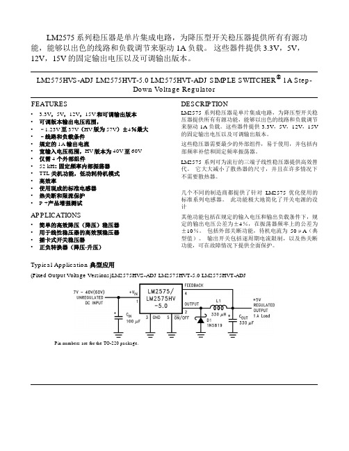
LM2575系列稳压器是单片集成电路,为降压型开关稳压器提供所有有源功能,能够以出色的线路和负载调节来驱动1A负载。
这些器件提供3.3V,5V,12V,15V的固定输出电压以及可调输出版本。
LM2575HVS-ADJ LM2575HVT-5.0 LM2575HVT-ADJ SIMPLE SWITCHER® 1A Step-Down Voltage RegulatorFEATURES• 3.3V,5V,12V,15V和可调输出版本•可调版本输出电压范围,•–1.23V至37V(HV版为57V)±4%最大•–线路和负载条件•规定的1A输出电流•宽输入电压范围,HV版本为40V至60V •仅需4个外部组件•52 kHz固定频率内部振荡器•TTL关机功能,低功耗待机模式•高效率•使用现成的标准电感器•热关断和限流保护•P +产品增强测试APPLICATIONS•简单的高效降压(降压)稳压器•用于线性稳压器的高效预稳压器•插卡式开关稳压器•正负转换器(降压-升压)DESCRIPTIONLM2575系列稳压器是单片集成电路,为降压型开关稳压器提供所有有源功能,能够以出色的线路和负载调节来驱动1A负载。
这些器件提供3.3V,5V,12V,15V 的固定输出电压以及可调输出版本。
这些稳压器需要最少的外部组件,易于使用,并包括内部频率补偿和固定频率振荡器。
LM2575系列可为流行的三端子线性稳压器提供高效替代。
它大大减小了散热器的尺寸,并且在许多情况下不需要散热器。
几个不同的制造商都提供了针对LM2575优化使用的标准系列电感器。
此功能极大地简化了开关电源的设计其他功能包括在规定的输入电压和输出负载条件下,规定的输出电压公差为±4%,在振荡器频率上的公差为±10%。
包括外部关断功能,待机电流为50μA(典型值)。
输出开关包括逐周期电流限制,以及热关断功能,可在故障情况下提供全面保护。
LM2575中文资料详解
LM2575 超详细中文介绍来源: | 发表于:2008年02月28日1 概述LM2575系列开关稳压集成电路是美国国家半导体公司生产的1A集成稳压电路,它内部集成了一个固定的振荡器,只须极少外围器件便可构成一种高效的稳压电路,可大大减小散热片的体积,而在大多数情况下不需散热片;内部有完善的保护电路,包括电流限制及热关断电路等;芯片可提供外部控制引脚。
是传统三端式稳压集成电路的理想替代产品。
此主题相关图片如下:该系列分为LM1575、LM2575及LM2575HV三个系列,其中LM1575为军品级产品,LM2575为标准电压产品,LM2575HV为高电压输入产品。
每一种产品系列均提供3.3V、5V、12V、15V及可调(ADJ)等多个电压档次产品。
除军品级产品外,其余两个系列均提供TO-200直脚、TO-220弯脚、塑封DIP-16脚、表面安装DIP-24脚、表面安装T)-263-5脚等多种封装形式,并分别用后缀T、Flow LB3、N、M、S表示。
对于5V输出的LM2575产品,不同的封装形式,其完整表示分别为LM2575T-5.0、LM2575T-5.0 Flow LB03、LM2575N-5.0、LM2575M-5.0、LM2575S-5.0。
LM2575T系列开关稳压集成电路芯片的主要参数如下:●最大输出电流:1A;●最大输入电压:LM1575/LM2575为45V;LM2575HV为63V;PCB下载站●输出电压:3.3V、5V、12V、ADJ(可调);●振荡频率:54kHz;●最大稳压误差:4%;●转换效率:75%~88%(不同的电压输出的效率不同);●工作温度范围:LM1575为-55℃~+150℃;LM2575/LM2575HV为-40℃~+125℃。
2 引脚功能图1是LM2575集成稳压器的两种引脚排列。
其引脚功能如下:VIN:未稳压电压输入端;PCB下载站OUTPUT:开关电压输出,接电感及快恢复二极管;GND:公共端;FEEDBACK:反馈输入端;ON/OFF:控制输入端,接公共端时,稳压电路工作;接高电平时,稳压电路停止。
LM2575中文资料详解

LM2575 超详细中文介绍来源: | 发表于:2008年02月28日1 概述LM2575系列开关稳压集成电路是美国国家半导体公司生产的1A集成稳压电路,它内部集成了一个固定的振荡器,只须极少外围器件便可构成一种高效的稳压电路,可大大减小散热片的体积,而在大多数情况下不需散热片;内部有完善的保护电路,包括电流限制及热关断电路等;芯片可提供外部控制引脚。
是传统三端式稳压集成电路的理想替代产品。
此主题相关图片如下:该系列分为LM1575、LM2575及LM2575HV三个系列,其中LM1575为军品级产品,LM2575为标准电压产品,LM2575HV为高电压输入产品。
每一种产品系列均提供、5V、12V、15V及可调(ADJ)等多个电压档次产品。
除军品级产品外,其余两个系列均提供TO-200直脚、TO-220弯脚、塑封DIP-16脚、表面安装DIP-24脚、表面安装T)-263-5脚等多种封装形式,并分别用后缀T、Flow LB3、N、M、S 表示。
对于5V输出的LM2575产品,不同的封装形式,其完整表示分别为、 Flow LB03、、、。
LM2575T系列开关稳压集成电路芯片的主要参数如下:●最大输出电流:1A;●最大输入电压:LM1575/LM2575为45V;LM2575HV为63V;此主题相关图片如下:●输出电压:、5V、12V、ADJ(可调);●振荡频率:54kHz;●最大稳压误差:4%;●转换效率:75%~88%(不同的电压输出的效率不同);●工作温度范围:LM1575为-55℃~+150℃;LM2575/LM2575HV为-40℃~+125℃。
2 引脚功能图1是LM2575集成稳压器的两种引脚排列。
其引脚功能如下:VIN:未稳压电压输入端;此主题相关图片如下:OUTPUT:开关电压输出,接电感及快恢复二极管;GND:公共端;FEEDBACK:反馈输入端;ON/OFF:控制输入端,接公共端时,稳压电路工作;接高电平时,稳压电路停止。
LM2575中文资料

LM2575 超详细中文介绍1 概述LM2575系列开关稳压集成电路是美国国家半导体公司生产的1A集成稳压电路,它内部集成了一个固定的振荡器,只须极少外围器件便可构成一种高效的稳压电路,可大大减小散热片的体积,而在大多数情况下不需散热片;内部有完善的保护电路,包括电流限制及热关断电路等;芯片可提供外部控制引脚。
是传统三端式稳压集成电路的理想替代产品。
此主题相关图片如下:该系列分为LM1575、LM2575及LM2575HV三个系列,其中LM1575为军品级产品,LM2575为标准电压产品,LM2575HV为高电压输入产品。
每一种产品系列均提供3.3V、5V、12V、15V及可调(ADJ)等多个电压档次产品。
除军品级产品外,其余两个系列均提供TO-200直脚、TO-220弯脚、塑封DIP-16脚、表面安装DIP-24脚、表面安装T)-263-5脚等多种封装形式,并分别用后缀T、Flow LB3、N、M、S表示。
对于5V输出的LM2575产品,不同的封装形式,其完整表示分别为LM2575T-5.0、LM2575T-5.0 Flow LB03、LM2575N-5.0、LM2575M-5.0、LM2575S-5.0。
LM2575T系列开关稳压集成电路芯片的主要参数如下:●最大输出电流:1A;●最大输入电压:LM1575/LM2575为45V;LM2575HV为63V;●输出电压:3.3V、5V、12V、ADJ(可调);●振荡频率:54kHz;●最大稳压误差:4%;●转换效率:75%~88%(不同的电压输出的效率不同);●工作温度范围:LM1575为-55℃~+150℃;LM2575/LM2575HV为-40℃~+125℃。
2 引脚功能图1是LM2575集成稳压器的两种引脚排列。
其引脚功能如下:VIN:未稳压电压输入端;OUTPUT:开关电压输出,接电感及快恢复二极管;GND:公共端;FEEDBACK:反馈输入端;ON/OFF:控制输入端,接公共端时,稳压电路工作;接高电平时,稳压电路停止。