k9f5608U0B
K9F1G08UOM数据手册

m A 5 5 15 15 1 10 10 20 20 1 µA 10 50 10 50
页 编 ICC2 程 擦除 ICC3 ISB1 等待状态电流 (TTL) 等待状态电流 (CMOS) 输入开漏电流 输出开漏电流
ISB2
IL1 IL0
-
-
±10 ±10
-
-
±10 ±10 VCC V +0.3 0.8 -
6. 命令/地址/ 数据复用端口: 7. 硬件数据保护:编程/擦除操作在电源转换时关闭。 8. 可靠的 CMOS 浮置门技术: --保证:100K 编程/ 擦除次数。 --数据保持时间: 10 年。 9. 命令寄存器操作 10. 为高速编程设置的缓冲编程操作。 11. 通电自动读操作。 12. 智能复制拷贝操作。 13.为防盗版而设置的唯一的 ID 保护。 14. 封装。 - K9F1GXXX0M-YCB0/YIB0 48 - Pin TSOP I (12 x 20 / 0.5 mm pitch) - K9F1G08U0M-VCB0/VIB0 48 - Pin WSOP I (12X17X0.7mm)
器件描述
三星 K9F1GXXX0M 提供了 128M*8Bit/64M*16Bit 的存储容量,另外还有 32 M 的空闲存储器,它是采用 NAND 技术的大容量、高可靠的 Flash 存储器。 它对 2112 字节一页(*8device )或者 1056 字(*16device)一页的写操作。典型 时间是 300 微秒。对 128 字节/64K 字一块的擦除时间是 50 纳秒。输出引脚可 以作为数据/地址/命令复用。每一页的数据读出时间也很快,平均每个字节只 需 50 纳秒。片内的写控制器,可以自动执行写操作和擦除功能,包括必要的脉 冲产生器,内部校验和冗余数据。 K9F1G08 提供了实时映像算法的纠错码,写 操作系统可以利用 K9F1G08U0M 扩展的 100K 编程/ 擦除。K9F1G08U0M 为大 容量存储,新型电可擦写的非易失性半导体存储器,提供了最优方案。
K9F2G08U0B

K9F2G08X0BINFORMATION IN THIS DOCUMENT IS PROVIDED IN RELATION TO SAMSUNG PRODUCTS, AND IS SUBJECT TO CHANGE WITHOUT NOTICE.NOTHING IN THIS DOCUMENT SHALL BE CONSTRUED AS GRANTING ANY LICENSE, EXPRESS OR IMPLIED, BY ESTOPPEL OR OTHERWISE,TO ANY INTELLECTUAL PROPERTY RIGHTS IN SAMSUNG PRODUCTS OR TECHNOLOGY. ALL INFORMATION IN THIS DOCUMENT IS PROVIDEDON AS "AS IS" BASIS WITHOUT GUARANTEE OR WARRANTY OF ANY KIND.1. For updates or additional information about Samsung products, contact your nearest Samsung office.2. Samsung products are not intended for use in life support, critical care, medical, safety equipment, or similar applications where Product failure could result in loss of life or personal or physical harm, or any military or defense application, or any governmental procurement to which special terms or provisions may apply.* Samsung Electronics reserves the right to change products or specification without notice.Document Title256M x 8 Bit NAND Flash Memory Revision HistoryThe attached data sheets are prepared and approved by SAMSUNG Electronics. SAMSUNG Electronics CO., LTD. reserve the rightto change the specifications. SAMSUNG Electronics will evaluate and reply to your requests and questions about device. If you have any questions, please contact the SAMSUNG branch office near your office.Revision No0.00.1RemarkAdvance PreliminaryHistory1. Initial issue2. Min. tCSD is changed from 10ns to 0nsDraft DateFeb. 15th 2008Apr. 22th 2008GENERAL DESCRIPTIONFEATURES• Voltage Supply- 2.7V device(K9F2G08B0B): 2.50V ~ 2.90V - 3.3V device(K9F2G08U0B): 2.70V ~ 3.60V • Organization- Memory Cell Array : (256M + 8M) x 8bit - Data Register : (2K + 64) x 8bit • Automatic Program and Erase - Page Program : (2K + 64)Byte - Block Erase : (128K + 4K)Byte • Page Read Operation- Page Size : (2K + 64)Byte - Random Read : 25µs(Max.) - Serial Access : 25ns(Min.)256M x 8 Bit NAND Flash Memory• Fast Write Cycle Time- Page Program time : 200µs(Typ.) - Block Erase Time : 1.5ms(Typ.)• Command/Address/Data Multiplexed I/O Port • Hardware Data Protection- Program/Erase Lockout During Power Transitions • Reliable CMOS Floating-Gate Technology-Endurance : 100K Program/Erase Cycles (with 1bit/512Byte ECC)- Data Retention : 10 Years • Command Driven Operation• Unique ID for Copyright Protection • Package :- K9F2G08X0B-PCB0/PIB0 : Pb-FREE PACKAGE 48 - Pin TSOP I (12 x 20 / 0.5 mm pitch)Offered in 256Mx8bit, the K9F2G08X0B is a 2G-bit NAND Flash Memory with spare 64M-bit. Its NAND cell provides the most cost-effective solution for the solid state application market. A program operation can be performed in typical 200µs on the (2K+64)Byte page and an erase operation can be performed in typical 1.5ms on a (128K+4K)Byte block. Data in the data register can be read out at 25ns cycle time per Byte. The I/O pins serve as the ports for address and data input/output as well as command input. The on-chip write controller automates all program and erase functions including pulse repetition, where required, and internal verification and margining of data. Even the write-intensive systems can take advantage of the K9F2G08X0B ′s extended reliability of 100K program/erase cycles by providing ECC(Error Correcting Code) with real time mapping-out algorithm. The K9F2G08X0B is an optimum solu-tion for large nonvolatile storage applications such as solid state file storage and other portable applications requiring non-volatility.PRODUCT LISTPart Number Vcc Range OrganizationPKG Type K9F2G08B0B-P 2.5 ~ 2.9V X8TSOP1K9F2G08U0B-P2.7 ~3.6vPIN DESCRIPTIONNOTE : Connect all V CC and V SS pins of each device to common power supply outputs. Do not leave V CC or V SS disconnected.Pin Name Pin FunctionI/O 0 ~ I/O 7DATA INPUTS/OUTPUTSThe I/O pins are used to input command, address and data, and to output data during read operations. The I/O pins float to high-z when the chip is deselected or when the outputs are disabled.CLECOMMAND LATCH ENABLEThe CLE input controls the activating path for commands sent to the command register. When active high, commands are latched into the command register through the I/O ports on the rising edge of the WE signal.ALEADDRESS LATCH ENABLEThe ALE input controls the activating path for address to the internal address registers. Addresses are latched on the rising edge of WE with ALE high.CECHIP ENABLEThe CE input is the device selection control. When the device is in the Busy state, CE high is ignored, and the device does not return to standby mode in program or erase operation.REREAD ENABLEThe RE input is the serial data-out control, and when active drives the data onto the I/O bus. Data is valid tREA after the falling edge of RE which also increments the internal column address counter by one.WEWRITE ENABLEThe WE input controls writes to the I/O port. Commands, address and data are latched on the rising edge of the WE pulse.WPWRITE PROTECTThe WP pin provides inadvertent program/erase protection during power transitions. The internal high volt-age generator is reset when the WP pin is active low.R/BREADY/BUSY OUTPUTThe R/B output indicates the status of the device operation. When low, it indicates that a program, erase or random read operation is in process and returns to high state upon completion. It is an open drain output and does not float to high-z condition when the chip is deselected or when outputs are disabled.Vcc POWERV CC is the power supply for device. Vss GROUNDN.CNO CONNECTIONLead is not internally connected.Product IntroductionThe K9F2G08X0B is a 2,112Mbit(2,214,592,512 bit) memory organized as 131,072 rows(pages) by 2,112x8 columns. Spare 64x8 columns are located from column address of 2,048~2,111. A 2,112-byte data register is connected to memory cell arrays accommo-dating data transfer between the I/O buffers and memory during page read and page program operations. The memory array is made up of 32 cells that are serially connected to form a NAND structure. Each of the 32 cells resides in a different page. A block consists of two NAND structured strings. A NAND structure consists of 32 cells. Total 1,081,344 NAND cells reside in a block. The program and read operations are executed on a page basis, while the erase operation is executed on a block basis. The memory array con-sists of 2,048 separately erasable 128K-byte blocks. It indicates that the bit by bit erase operation is prohibited on the K9F2G08X0B. The K9F2G08X0B has addresses multiplexed into 8 I/Os. This scheme dramatically reduces pin counts and allows system upgrades to future densities by maintaining consistency in system board design. Command, address and data are all written through I/O's by bringing WE to low while CE is low. Those are latched on the rising edge of WE. Command Latch Enable(CLE) and Address Latch Enable(ALE) are used to multiplex command and address respectively, via the I/O pins. Some commands require one bus cycle. For example, Reset Command, Status Read Command, etc require just one cycle bus. Some other commands, like page read and block erase and page program, require two cycles: one cycle for setup and the other cycle for execution. The 264M byte physical space requires 29 addresses, thereby requiring five cycles for addressing : 2 cycles of column address, 3 cycles of row address, in that order. Page Read and Page Program need the same five address cycles following the required command input. In Block Erase oper-ation, however, only the three row address cycles are used. Device operations are selected by writing specific commands into the command register. Table 1 defines the specific commands of the K9F2G08X0B.Table 1. Command SetsFunction1st Cycle2nd Cycle Acceptable Command during Busy Read 00h30hRead for Copy Back00h35hRead ID90h-Reset FFh-OPage Program80h10hTwo-Plane Page Program(1)80h---11h81h---10hCopy-Back Program85h10hTwo-Plane Copy-Back Program(1)85h---11h81h---10hBlock Erase60h D0hTwo-Plane Block Erase60h---60h D0hRandom Data Input(2)85h-Random Data Output(2)05h E0hRead Status70h-ORead Status 2F1h-ONOTE : 1. Any command between 11h and 81h is prohibited except 70h/F1h and FFh.2. Random Data Input/Output can be executed in a page.Caution : Any undefined command inputs are prohibited except for above command set of Table 1.DC AND OPERATING CHARACTERISTICS (Recommended operating conditions otherwise noted.)NOTE : 1. V IL can undershoot to -0.4V and V IH can overshoot to V CC +0.4V for durations of 20 ns or less. 2. Typical value is measured at Vcc=2.7V/3.3V, T A =25°C. Not 100% tested.ParameterSymbol Test Conditions 2.7V3.3V UnitMinTypMaxMinTypMaxOperating CurrentPage Read withSerial Access I CC 1tRC=25nsCE=V IL, I OUT =0mA-1530-1530mAProgramI CC 2-EraseI CC 3-Stand-by Current(TTL)I SB 1CE=V IH , WP=0V/V CC --1--1Stand-by Current(CMOS)I SB 2CE=V CC -0.2, WP=0V/V CC -1050-1050µAInput Leakage Current I LI V IN =0 to Vcc(max)--±10--±10Output Leakage Current I LO V OUT =0 to Vcc(max)--±10--±10Input High VoltageV IH (1)-Vcc-0.4-Vcc+0.3 2.0-Vcc+0.3V Input Low Voltage, All inputs V IL (1)--0.3-0.5-0.3-0.8Output High Voltage Level V OH K9F2G08B0B: I OH=-100µAK9F2G08U0B: I OH =-400µA Vcc-0.42.4--Output Low Voltage Level V OL K9F2G08B0B: I OL=100µA K9F2G08U0B: I OL =2.1mA --0.4--0.4Output Low Current(R/B)I OL (R/B)K9F2G08B0B: V OL =0.1V K9F2G08U0B: V OL =0.4V34810-mA RECOMMENDED OPERATING CONDITIONS(Voltage reference to GND, K9F2G08X0B-XCB0 :T A =0 to 70°C, K9F2G08X0B-XIB0:T A =-40 to 85°C)Parameter Symbol 2.7V3.3V Unit Min Typ.Max Min Typ.Max Supply Voltage V CC 2.5 2.7 2.9 2.7 3.3 3.6V Supply VoltageV SSVABSOLUTE MAXIMUM RATINGSNOTE :1. Minimum DC voltage is -0.6V on input/output pins. During transitions, this level may undershoot to -2.0V for periods <30ns. Maximum DC voltage on input/output pins is V CC +0.3V which, during transitions, may overshoot to V CC +2.0V for periods <20ns.2. Permanent device damage may occur if ABSOLUTE MAXIMUM RATINGS are exceeded. Functional operation should be restricted to the conditions as detailed in the operational sections of this data sheet. Exposure to absolute maximum rating conditions for extended periods may affect reliability.ParameterSymbol Rating Unit Voltage on any pin relative to VSSV CC -0.6 to +4.6VV IN -0.6 to +4.6V I/O-0.6 to Vcc + 0.3 (< 4.6V)Temperature Under BiasK9F2G08X0B-XCB0T BIAS -10 to +125°C K9F2G08X0B-XIB0-40 to +125Storage Temperature K9F2G08X0B-XCB0T STG-65 to +150°CK9F2G08X0B-XIB0Short Circuit CurrentI OS5mACAPACITANCE (T A =25°C, V CC =2.7V/3.3V, f=1.0MHz)NOTE : Capacitance is periodically sampled and not 100% tested.ItemSymbol Test ConditionMin Max Unit Input/Output Capacitance C I/O V IL =0V -10pF Input CapacitanceC INV IN =0V-10pFVALID BLOCKNOTE :1. The device may include initial invalid blocks when first shipped. Additional invalid blocks may develop while being used. The number of valid blocks is presented with both cases of invalid blocks considered. Invalid blocks are defined as blocks that contain one or more bad bits. Do not erase or pro-gram factory-marked bad blocks. Refer to the attached technical notes for appropriate management of invalid blocks.2. The 1st block, which is placed on 00h block address, is guaranteed to be a valid block up to 1K program/erase cycles with 1bit/512Byte ECC.3. The number of valid block is on the basis of single plane operations, and this may be decreased with two plane operations.Parameter Symbol Min Typ.Max Unit K9F2G08X0BN VB2,008-2,048BlocksAC TEST CONDITION(K9F2G08X0B-XCB0 :T A =0 to 70°C, K9F2G08X0B-XIB0:T A =-40 to 85°C,K9F2G08B0B: Vcc=2.5V~2.9V, K9F2G08U0B: Vcc=2.7V~3.6V unless otherwise noted)ParameterK9F2G08X0B Input Pulse Levels 0V to Vcc Input Rise and Fall Times 5ns Input and Output Timing Levels Vcc/2Output Load1 TTL GATE and CL=50pFMODE SELECTIONNOTE : 1. X can be V IL or V IH.2. WP should be biased to CMOS high or CMOS low for standby.CLE ALE CE WERE WP ModeH L L H X Read Mode Command Input L H L H X Address Input(5clock)H L L H H Write Mode Command Input L H L H H Address Input(5clock)L L L HH Data Input L L L H X Data Output X X X X H X During Read(Busy)X X X X X H DuringProgram(Busy)X X X X X H DuringErase(Busy)X X (1)X X X L Write Protect XXHXX0V/V CC (2)Stand-byProgram / Erase CharacteristicsParameter Symbol Min Typ Max Unit Program Time t PROG-200700µs Dummy Busy Time for Two-Plane Page Program t DBSY-0.51µs Number of Partial Program Cycles Nop--4cycles Block Erase Time t BERS- 1.510ms NOTE :1. Typical value is measured at Vcc=3.3V, T A=25°C. Not 100% tested.2. Typical program time is defined as the time within which more than 50% of the whole pages are programmed at3.3V Vcc and 25°C temperature.AC Timing Characteristics for Command / Address / Data InputParameter Symbol Min Max Unit CLE Setup Time t CLS(1)12-ns CLE Hold Time t CLH5-nsCE Setup Time t CS(1)20-nsCE Hold Time t CH5-nsWE Pulse Width t WP12-ns ALE Setup Time t ALS(1)12-ns ALE Hold Time t ALH5-ns Data Setup Time t DS(1)12-ns Data Hold Time t DH5-ns Write Cycle Time t WC25-nsWE High Hold Time t WH10-ns Address to Data Loading Time t ADL(2)100-ns NOTES : 1. The transition of the corresponding control pins must occur only once while WE is held low2. tADL is the time from the WE rising edge of final address cycle to the WE rising edge of first data cycleAC Characteristics for OperationParameter Symbol Min Max Unit Data Transfer from Cell to Register t R-25µs ALE to RE Delay t AR10-ns CLE to RE Delay t CLR10-ns Ready to RE Low t RR20-ns RE Pulse Width t RP12-ns WE High to Busy t WB-100ns Read Cycle Time t RC25-ns RE Access Time t REA-20ns CE Access Time t CEA-25ns RE High to Output Hi-Z t RHZ-100ns CE High to Output Hi-Z t CHZ-30ns CE High to ALE or CLE Don’t Care t CSD0-ns RE High to Output Hold t RHOH15-ns RE Low to Output Hold t RLOH5-ns CE High to Output Hold t COH15-ns RE High Hold Time t REH10-ns Output Hi-Z to RE Low t IR0-ns RE High to WE Low t RHW100-ns WE High to RE Low t WHR60-ns Device Resetting Time(Read/Program/Erase)t RST-5/10/500(1)µs NOTE : 1. If reset command(FFh) is written at Ready state, the device goes into Busy for maximum 5µs.NAND Flash Technical NotesIdentifying Initial Invalid Block(s)Initial Invalid Block(s)Initial invalid blocks are defined as blocks that contain one or more initial invalid bits whose reliability is not guaranteed by Samsung.The information regarding the initial invalid block(s) is called the initial invalid block information. Devices with initial invalid block(s)have the same quality level as devices with all valid blocks and have the same AC and DC characteristics. An initial invalid block(s)does not affect the performance of valid block(s) because it is isolated from the bit line and the common source line by a select tran-sistor. The system design must be able to mask out the initial invalid block(s) via address mapping. The 1st block, which is placed on 00h block address, is guaranteed to be a valid block up to 1K program/erase cycles with 1bit /512Byte ECC.All device locations are erased(FFh) except locations where the initial invalid block(s) information is written prior to shipping. The ini-tial invalid block(s) status is defined by the 1st byte in the spare area. Samsung makes sure that either the 1st or 2nd page of every initial invalid block has non-FFh data at the column address of 2048. Since the initial invalid block information is also erasable in most cases, it is impossible to recover the information once it has been erased. Therefore, the system must be able to recognize the initial invalid block(s) based on the original initial invalid block information and create the initial invalid block table via the following suggested flow chart(Figure 3). Any intentional erasure of the original initial invalid block information is prohibited.*Check "FFh" at the column address 2048 Figure 3. Flow chart to create initial invalid block tableStartSet Block Address = 0Check "FFh"Increment Block AddressLast Block ?EndNoYesYesCreate (or update)NoInitialof the 1st and 2nd page in the blockInvalid Block(s) TableNAND Flash Technical Notes (Continued)Program Flow ChartStartI/O 6 = 1 ?I/O 0 = 0 ?No*Write 80hWrite AddressWrite DataWrite 10hRead Status RegisterProgram Completedor R/B = 1 ?Program ErrorYesNoYes: If program operation results in an error, map out the block including the page in error and copy thetarget data to another block.*Error in write or read operationWithin its life time, additional invalid blocks may develop with NAND Flash memory. Refer to the qualification report for the actual data.The following possible failure modes should be considered to implement a highly reliable system. In the case of status read fail-ure after erase or program, block replacement should be done. Because program status fail during a page program does not affect the data of the other pages in the same block, block replacement can be executed with a page-sized buffer by finding an erased empty block and reprogramming the current target data and copying the rest of the replaced block. In case of Read, ECC must be employed. To improve the efficiency of memory space, it is recommended that the read or verification failure due to single bit error be reclaimed by ECC without any block replacement. The said additional block failure rate does not include those reclaimed blocks.Failure ModeDetection and Countermeasure sequenceWrite Erase Failure Status Read after Erase --> Block Replacement Program Failure Status Read after Program --> Block Replacement ReadSingle Bit FailureVerify ECC -> ECC CorrectionECC: Error Correcting Code --> Hamming Code etc. Example) 1bit correction & 2bit detectionNAND Flash Technical Notes (Continued)Within a block, the pages must be programmed consecutively from the LSB(least significant bit) page of the block to the MSB(most significant bit) pages of the block. Random page address programming is prohibited. In this case, the definition of LSB page is the LSB among the pages to be programmed. Therefore, LSB doesn't need to be page 0.From the LSB page to MSB page DATA IN: Data (1)Data (64)(1)(2)(3)(32)(64)Data register Page 0Page 1Page 2Page 31Page 63Ex.) Random page program (Prohibition)DATA IN: Data (1)Data (64)(2)(32)(3)(1)(64)Data registerPage 0Page 1Page 2Page 31Page 63Addressing for program operation::::Read ID OperationCECLEWEALERE90hRead ID CommandMaker Code Device Code00h ECht REAAddress 1cycleI/Oxt ARDevice Device Code (2nd Cycle)3rd Cycle 4th Cycle 5th Cycle K9F2G08B0B Same as K9F2G08U0BK9F2G08U0BDAh10h95h44hDevice 4th cyc.Code3rd cyc.5th cyc.4th ID DataDescription I/O7 I/O6I/O5 I/O4 I/O3I/O2I/O1 I/O0Page Size(w/o redundant area ) 1KB2KB4KB8KB0 00 11 01 1Block Size(w/o redundant area ) 64KB128KB256KB512KB0 00 11 01 1Redundant Area Size ( byte/512byte) 8161Organization x8x161Serial Access Minimum 50ns/30ns25nsReservedReserved1111ID Definition TableDescription1st Byte 2nd Byte 3rd Byte 4th Byte 5th Byte Maker CodeDevice CodeInternal Chip Number, Cell Type, Number of Simultaneously Programmed Pages, Etc Page Size, Block Size,Redundant Area Size, Organization, Serial Access Minimum Plane Number, Plane Size3rd ID DataDescription I/O7 I/O6I/O5 I/O4I/O3 I/O2I/O1 I/O0Internal Chip Number 12480 00 11 01 1Cell Type 2 Level Cell4 Level Cell8 Level Cell16 Level Cell0 00 11 01 1Number ofSimultaneouslyProgrammed Pages 12480 00 11 01 1Interleave Program Between multiple chips Not SupportSupport1Cache Program Not SupportSupport15th ID DataDescription I/O7I/O6 I/O5 I/O4I/O3 I/O2 I/O1I/O0Plane Number 12480 00 11 01 1Plane Size(w/o redundant Area) 64Mb128Mb256Mb512Mb1Gb2Gb4Gb8Gb0 0 00 0 10 1 00 1 11 0 01 0 11 1 01 1 1Reserved 0 0 0Figure 7. Random Data Output In a PageAddress 00hData OutputR/B RE t R30hAddress 05hE0h5Cycles2Cycles Data OutputData Field Spare Field Data Field Spare FieldI/OxCol. Add.1,2 & Row Add.1,2,3PAGE PROGRAMThe device is programmed basically on a page basis, but it does allow multiple partial page programming of a word or consecutive bytes up to 2,112, in a single page program cycle. The number of consecutive partial page programming operation within the same page without an intervening erase operation must not exceed 4 times for a single page. The addressing should be done in sequential order in a block. A page program cycle consists of a serial data loading period in which up to 2,112bytes of data may be loaded into the data register, followed by a non-volatile programming period where the loaded data is programmed into the appropriate cell.The serial data loading period begins by inputting the Serial Data Input command(80h), followed by the five cycle address inputs and then serial data loading. The words other than those to be programmed do not need to be loaded. The device supports random data input in a page. The column address for the next data, which will be entered, may be changed to the address which follows random data input command(85h). Random data input may be operated multiple times regardless of how many times it is done in a page.The Page Program confirm command(10h) initiates the programming process. Writing 10h alone without previously entering the serial data will not initiate the programming process. The internal write state controller automatically executes the algorithms and tim-ings necessary for program and verify, thereby freeing the system controller for other tasks. Once the program process starts, the Read Status Register command may be entered to read the status register. The system controller can detect the completion of a pro-gram cycle by monitoring the R/B output, or the Status bit(I/O 6) of the Status Register. Only the Read Status command and Reset command are valid while programming is in progress. When the Page Program is complete, the Write Status Bit(I/O 0) may be checked(Figure 8). The internal write verify detects only errors for "1"s that are not successfully programmed to "0"s. The command register remains in Read Status command mode until another valid command is written to the command register.Figure 8. Program & Read Status Operation80hR/B Address & Data Input I/O0PassData10h70hFailt PROGI/OxCol. Add.1,2 & Row Add.1,2,3"0""1"Col. Add.1,2Figure 9. Random Data Input In a Page80hR/B Address & Data Input I/O0Pass10h70hFailt PROG85hAddress & Data InputI/OxCol. Add.1,2 & Row Add1,2,3Col. Add.1,2 DataData"0""1"Copy-Back ProgramCopy-Back program with Read for Copy-Back is configured to quickly and efficiently rewrite data stored in one page without data re-loading when the bit error is not in data stored. Since the time-consuming re-loading cycles are removed, the system performance is improved. The benefit is especially obvious when a portion of a block is updated and the rest of the block also needs to be copied to the newly assigned free block. Copy-Back operation is a sequential execution of Read for Copy-Back and of copy-back program with the destination page address. A read operation with "35h" command and the address of the source page moves the whole 2,112-byte data into the internal data buffer. A bit error is checked by sequential reading the data output. In the case where there is no bit error,the data do not need to be reloaded. Therefore Copy-Back program operation is initiated by issuing Page-Copy Data-Input command (85h) with destination page address. Actual programming operation begins after Program Confirm command (10h) is issued. Once the program process starts, the Read Status Register command (70h) may be entered to read the status register. The system control-ler can detect the completion of a program cycle by monitoring the R/B output, or the Status bit(I/O 6) of the Status Register. When the Copy-Back Program is complete, the Write Status Bit(I/O 0) may be checked(Figure 10 & Figure 11). The command register remains in Read Status command mode until another valid command is written to the command register.During copy-back program, data modification is possible using random data input command (85h) as shown in Figure11.Figure 10. Page Copy-Back Program Operation00hR/B Add.(5Cycles)I/O0Pass85h 70h Failt PROGAdd.(5Cycles) t R Source Address Destination Address35h10h I/OxCol. Add.1,2 & Row Add.1,2,3Col. Add.1,2 & Row Add.1,2,3Figure 11. Page Copy-Back Program Operation with Random Data Input00hR/B Add.(5Cycles)85h 70ht PROGAdd.(5Cycles) t RSource AddressDestination AddressData 35h10h 85hData Add.(2Cycles) There is no limitation for the number of repetition.I/OxCol. Add.1,2 & Row Add.1,2,3Col. Add.1,2 & Row Add.1,2,3Col. Add.1,2Note : Copy-Back Program operation is allowed only within the same memory plane."0""1"Figure 13. Block Erase OperationBLOCK ERASEThe Erase operation is done on a block basis. Block address loading is accomplished in three cycles initiated by an Erase Setup command(60h). Only address A 18 to A 28 is valid while A 12 to A 17 is ignored. The Erase Confirm command(D0h) following the block address loading initiates the internal erasing process. This two-step sequence of setup followed by execution command ensures that memory contents are not accidentally erased due to external noise conditions.At the rising edge of WE after the erase confirm command input, the internal write controller handles erase and erase-verify. When the erase operation is completed, the Write Status Bit(I/O 0) may be checked. Figure 13 details the sequence.60hRow Add 1,2,3R/B Address Input(3Cycle)I/O0PassD0h70hFailt BERSI/Ox"0""1"Two-Plane Page ProgramTwo-Plane Page Program is an extension of Page Program, for a single plane with 2,112 byte page registers. Since the device is equipped with two memory planes, activating the two sets of 2,112 byte page registers enables a simultaneous programming of two pages.After writing the first set of data up to 2,112 byte into the selected page register, Dummy Page Program command (11h) instead of actual Page Program command (10h) is inputted to finish data-loading of the first plane. Since no programming process is involved,R/B remains in Busy state for a short period of time(tDBSY). Read Status command (70h/F1h) may be issued to find out when the device returns to Ready state by polling the Ready/Busy status bit(I/O 6). Then the next set of data for the other plane is inputted after the 81h command and address sequences. After inputting data for the last plane, actual True Page Program(10h) instead of dummy Page Program command (11h) must be followed to start the programming process. The operation of R/B and Read Status is the same as that of Page Program. Althougth two planes are programmed simultaneously, pass/fail is not available for each page when the program operation completes. Status bit of I/O 0 is set to "1" when any of the pages fails. Restriction in addressing with Two-Plane Page Program is shown is Figure14.。
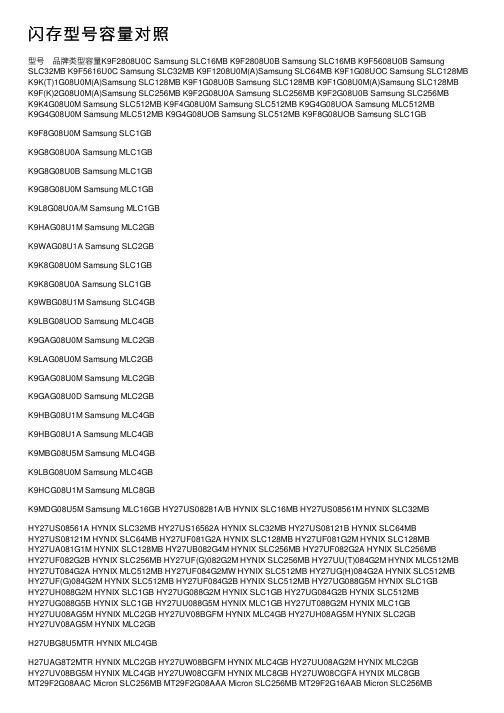
闪存型号容量对照
K9GAG08U0M Samsung MLC2GB
K9GAG08U0D Samsung MLC2GB
K9HBG08U1M Samsung MLC4GB
K9HBG08U1A Samsung MLC4GB
K9MBG08U5M Samsung MLC4GB
K9F8G08U0M Samsung SLC1GB
K9G8G08U0A Samsung MLC1GB
K9amsung MLC1GB
K9L8G08U0A/M Samsung MLC1GB
K9HAG08U1M Samsung MLC2GB
MT29F2G08X Micron SLC256MB MT29F2G08AAB Micron SLC256MB MT29F4G08MAA Micron MLC512MB MT29F4G08AAA Micron SLC512MB
MT29F4G08AAA(1)Micron SLC512MB MT29F8G08FAB Micron SLC1GB MT29F8G08DAA Micron SLC1GB MT29F8G08QAA Micron MLC1GB MT29F8G16MAA Micron MLC1GB MT29F128G08CJWAAAWC Micron MLC16GB MT29F8G08MAD Micron MLC1GB MT29F8G08BAA Micron SLC1GB MT29F8G08MAA Micron MLC1GB MT29F16G08FAA Micron SLC2GB MT29F16G08QAA Micron MLC2GB MT29F16G08MAA Micron MLC2GB MT29F16G08TAA Micron MLC2GB MT29F32G08QAA Micron MLC4GB MT29F32G08CBAAAWP Micron MLC4GB MT29F32G09CFAAA Micron MLC8GB MT29F32G08TAA Micron MLC4GB MT29F32G08FAA Micron SLC4GB MT29F32G08TAA1Micron MLC4GB MT29F64G08TAA Micron MLC8GB MT29F64G08MAA Micron MLC8GB JS29F02G08AAA intel SLC256MB JS29F04G08FANB3intel MLC512MB JS29F8G08CANCI intel MLC1GB JS29F16G08CANCI intel MLC2GB JS29F16G08CANC2intel MLC2GB JS29F08G08CANC1intel MLC1GB JS29F08G08AAMB2intel MLC1GB JS29F16G08CAMB2intel SLC2GB JS29F16G08AAMC1intel MLC2GB JS29F32G08CAMC1intel MLC4GB JS29F32G08FAMB2intel MLC4GB JS29F32G08AAMDB intel MLC4GB JS29F32G08AAMD2intel MLC4GB JS29F64G08CAMDB intel MLC8GB JS29F64G08CAMD1intel MLC8GB JS29F128G08FAMC1intel MLC16GB TC58128(A)FT Toshiba SLC16MB TC58256(A)FT Toshiba SLC32MB TC58DVM82A1FT Toshiba SLC32MB TC58512(A)FT Toshiba SLC64MB TC58DVM92A1FT Toshiba SLC64MB
焊接件丝印参照表
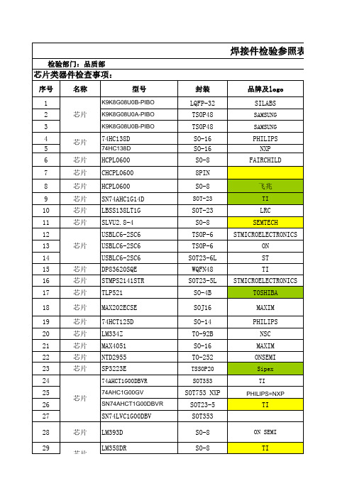
107
芯片 LM4040DIM3-2.5
108
芯片 S818A33AMC
109
芯片 74HC4052D
110
ISMB5934BT3
111
B0505LS-1W
DC 模块
24PIN-QEN SOT-23 5PIN SO-16 2PIN
b0505ls
MORNSUN SILABS
TI SII NXP
MICRODC
SO-8
MAXIM
87
芯片 74HC14D
14PIN
NXP
88
芯片 AD8628ART
5PIN
AD
89
芯片 IRF7416
8PIN
IRF
90
芯片 AD712JR
SO-8
ADI
91
芯片 ADUM1400CRW
16PIN
AD
92
芯片 MAX1680
8PIN
MAXIM
93
芯片 TL431ACDBZR
SOT-23
8PIN
166
芯片 OP2347
8PIN
167
芯片 OPA2227
8PIN
168
芯片 TL061
8PIN
169
芯片 ADM101E
10PIN
170
芯片 TPS76950DBVT
5PIN
171
芯片 TPS76350
5PIN
172
芯片 C8051F064
100PIN
173
C8051F069
174
芯片 OPA350
ALTERA
69
芯片 IS62WV5128BLL-55H1I
ZORAN方案资料

2013年8月7日星期三
1-6.2
训练的发展路程:
训练 10P 训练 9M 训练 6P 训练 7P 训练 8P 训练 10M 训练 9S
训练 6M
训练 7E
训练 8M 训练 9E
训练 6E
训练 7M
训练 8S
2003
2004
2005
2006
2007
Zoran Proprietary and Confidential Copyright 2006 Zoran Corporation All Rights Reserved
272个大头针 , 17x 17/0.8 毫米
#自由地带领
276个大头针 , 19x 19/1.0 毫米
#自由地带领
感应器
透镜马 达 重复 PWM
12 一点点描绘数据 ≦ 16 超级的图素 4 移植 M1(一 ~ D) M2(一 ~ D) M3(一 ~ D) M4(一 ~ D) 引起信号 第二引起控制 相片-发现者输入 8 PWM(0~7)
2013年8月7日星期三
4-6.2
训练 6 系列:
训练 6 系列家族成员:
6e (最高支持 3M 感应器) ► 训练 6m (最高支持 16M 感应器) ► 训练 6p (最高支持 16M 感应器) ► 训练 6mcm (最高支持 16M 感应器)
► 训练
Zoran Proprietary and Confidential Copyright 2006 Zoran Corporation All Rights Reserved
2013年8月7日星期三
2-6.2
客户常用到的训练系列
1,低端的互补型金属氧化半导体相机或者 ► 训练 6e ( ZR36440 ,最高支持 3M 感应器) DV: 6m(ZR36441, 最高支持16M Sensor) ► Coach 2,带 MP4 录像功能的相机或者 DV:
U盘 维修
U盘(优盘)的故障表现及数据恢复1、U盘毫无反应:有可能U盘插口针脚断裂,晶震坏,稳压三极管电路不能工作,数据全部可以恢复。
2。
有盘符,提示请插入磁盘:<1>U盘主控内部系统文件损坏,数据全部可以恢复。
一般更换相同的主控即可,可是找一个相同的U 盘,主控相同,U盘容量相同,实在不易,为此我公司引进世界先进技术,直接读取FLASH芯片内的数据,达到快速恢复文件,欢迎咨询<2>U盘FLASH芯片存在坏块区,数据恢复可以完全恢复或部份恢复,视具体损坏情况来定!3。
有盘符但提示未格式化:U盘存在坏扇区或引导扇区有问题,如无重要数据格式化之后便可使用。
可做数据恢复,而且数据恢复的结果十分完整,这种情况一般都是使用不当造成的故障,如热插拔之类的误操作,USB接口电压等,尽量使用时正常使用。
4。
无盘符提示无法识别的USB设备:晶震或稳压三极管损坏,这种情况数据全部可以恢复。
5。
逻辑类的问题:无盘符,但能检到U盘,提示格式化等,数据可以恢复。
常见flash芯片类型列表H27UCG8VFM HY27UG088G5M HY27SA161G1M HY27SS08121MH27U2G8T2M HY27UH08AG5M HY27UF081G2A HY27SS16121MH27U2G8T2M HY27UH08AG5B HY27UF161G2A HY27US08121MHN29V2G74W30 HY27UK08BGFM HY27UF081G2M HY27US16121MH27UBG8H5M HY27UH08BGFB HY27UF161G2M HY27US08561AH27U8G8F2M HY27UT084G2A HY27SF081G2M HY27US16561AH27UAG8G5M HY27UT084G2M HY27SF161G2M HY27SS08561AH27UBG8T5M HY27UU088G5M HY27UF082G2A HY27SS16561AHY27US08281A HY27UT088G2M HY27UF162G2A HY27US08561MHY27US08561A HY27UT088G2A HY27UF082G2B HY27US16561MHY27US08561M HY27UV08AG5M HY27UF162G2B HY27SS08561MHY27US08121A HY27UV08BG5M HY27UF084G2B HY27SS16561MHY27US08121M HY27UV08BGFM HY27UF164G2B HY27US08281AHY27UA081G1M HY27UV08BGFA HY27UF082G2M HY27US16281AHY27UA081G4M HY27UU08AG5M HY27UF162G2M HN29W12811T-60HY27UB082G4M HY27UU08AG5A HY27UH088G2M HN29V25691BTHY27UF081G2A HY27UW08BGFM HY27UH088GDM HN29V51211T-50HY27UF081G2M HY27UW08CGFM HY27UG088G5B HN29V1G91T-30HY27UF082G2A Hynix InkDie HY27UG088G5M HY27UF164G2B(x16)HY27UF082G2M H27UAG8T2M HY27UH08AG5M HYF33DS512804(5)BTC HY27UF082G2B H27UCG8V5M HY27UK08BGFM HYF33DS512804(5)BTC HY27UF084G2B HY27SF082G2B HY27US081G1M HYF33DS512804(5)BTC HY27UG088G5B HY27SF162G2B HY27US161G1M HYF33DS512804(5)BTC HY27UF084G2M HY27SF081G2A HY27US08121A HYF33DS1G800CTIHY27UG084G2M HY27SF161G2A HY27US16121A HYF33DS1G800CTIHY27UH084G2M HY27U(s)A081G1M HY27SS08121A HY27US16562AHY27UH088G2M HY27UA161G1M HY27SS16121A HY27SS081G1XI29F04G08AAA I29F32G08CAMCI FTGM40A2GK3WG FTNL41B8GK3PGI29F08G08AAMB2 I29F64G08FAMC1 FBNL41B32K3P4 FTNL41B8GK3PGI29F08G08AAMBI PF79BL1208BSG FBNL41B8GK3P2 FTNL41B8GK3PGI29F16G08AAMCI PF79AL1208BS FTNL41BHGK3W4 R1FV04G13RSA-3I29F16G08MAA DFT512W08B-P1 FBNL41B8GK3W3 R1FV04G13RSA-3_2ASU4GA30GT K9F2G08U0M K9WBG08U1M K9L8G08U0MASU2GA30GT K9F2G08U0M K9NBG08U5A K9LAG08U0MK9F2808U0B K9K2G08U0M K9NCG08U5M K9LAG08U0A_BK9F5608U0B K9GAG08U0A K9G2G08U0M K9HBG08U1AK9F1208U0A K9GAG08U0D K9G4G08U0A K9LBG08U0MK9F1208U0B K9K4G08U0M K9G8G08U0A K9HAG08U1MK9F1208U0C K9F4G08U0A K9G8G08U0M K9HBG08U1MK9K1G08U0M K9F8G08U0M K9L8G08U1M K9HCG08U1MK9E2G08U1M K9K8G08U0A K9LBG08U0D K9MDG08U5MK9F1G16U0M K9KAG08U0M K9HCG08U1M K9MBG08U5MK9F1G08U0A K9W8G08U1M K9HCG08U1D K9MCG08U5MK9F1G08U0B K9WAG08U1A K9LAG08U1M K9GAG08U0MK9F1G08U0M K9LBG08U1M K9HCG08U5M K9F5616U0C(x16)K9F2G08U0A K9F1208U0M K9F5616U0C K9K4G16Q0MK9F1G16Q0M K9F2808U0 K9G8G08U0M K9XXG08UXMK9F1G08 K9F5608U0B K9LAG08U0M K9K4G16U0MK9F1G16U0M K9F5616U0B K9HBG08U1M K9K8G08U0MK9F2G08U0A K9F5608D0C K9MCG08U5M K9WAG08U1MK9F2G16U0M K9F5616D0C K9K1G08U0M K9K2G08Q0MK9F2G08U0M K9F5608U0C K9K4G08Q0M K9K2G16Q0MK9XXG08UXM K9XXG16UXM K9K2G08U0M K9F1G08Q0MNAND128W3A2BN6E NAND08GW3C2B NAND512R3A NAND04GW4B2DNAND256W3A2BN6E NAND16GW3C4B NAND512W3A NAND08GW3B2CNAND512W3A0AN6 NAND01GW3B2B NAND512R4A NAND08GR4B2CNAND01GW3A0AN6 NAND01GR4B2B NAND512W4A NAND08GW4B2CNAND01GW3B2AN6 NAND01GW4B2B NAND01GR3A NAND08GW3C2ANAND01GW3B2BN6 NAND02GW3B2C NAND01GW3A NAND16GW3C4ANAND02GW3B2AN6 NAND02GR4B2C NAND01GR4A NAND08GW3C2BNAND02GW3B2D NAND02GW4B2C NAND01GW4A NAND08GW3D2ANAND02GW3B2CN6 NAND01GW3B2C NAND02GW3B2D NAND512R3A2DNAND04GW3B2DN6 NAND01GR4B2C NAND02GR4B2D NAND512W3A2DNAND04GW3B2BN6 NAND01GW4B2C NAND02GW4B2D NAND512R4A2DNAND08GW3B2CN6 NAND128R3A NAND04GW3C2A NAND512W4A2DNAND08GW3B2AN6 NAND128W3A NAND04GA3C2A NAND01GR3A2CNAND04GW3C2AN1 NAND256R3A NAND04GW3B2B NAND01GW3A2CNAND08GW3C2AN1 NAND256W3A NAND08GW3B2A NAND01GR4A2CNAND08GW3B2CN6 NAND256R4A NAND04GW3B2D NAND01GW4A2CNAND04GW3C2B NAND256W4A NAND04GR4B2D NAND04GW3C2BNAND08GW3F2A NAND16GW3F2A NAND08GW3C2BMT29F8G08MAA MT29F64G08TAA MT29F4G08ABC MT29F4G08BABMT29F8G16MAA MT29F32G08BAAA MT29F32G08FAA MT29F8G08FABMT29F16G08QAA MT29F64G08CFAAA MT29F8G08BAA MT29F4G16BABMT29F2G08AAC MT29F4G08ABC MT29F8G08DAA MT29F16G08QAA(DUAL) MT29F32G08TAA MT29F2G08AAA MT29F16G08FAA MT29F2G08ABCMT29F2G16AAC MT29F2G16ABD MT29F4G08MAA MT29F32G08TAA-BMT29F2G16ABC MT29F2G08AAB_C MT29F4G08MAA_2 MT29F128G08CJAAA MT29F4G08BBC MT29F4G08AAA_C MT29F8G08MAD MT29F4G08BACMT29F8G08MBD MT29F4G08BAB_C MT29F8G08MAD MT29F8G08FACMT29F4G08AAA MT29F8G08FAB_C MT29F2G08AAD MT29F16G08CBABAMT29F8G08DAA MT29F8G08MAD MT29F2G08AAB MT29F32G08CBABAMT29F16G08MAA MT29F8G08AAA MT29F2G08ABB MT29F8G08BAAMT29F16G08MAA MT29F16G08DAA MT29F2G16AAB MT29F16G08FAAMT29F32G08QAA MT29F2G08ABC MT29F2G16ABBSDTNFCH-512 SDTNKGHSM-8192 SDMLC-1GB-I SDUNIHHSM-8192(16bit)SDTNFCH-1024 SDMLC-16384-I SDTNLLBHSM-32768 SDTNIHHSM-4096(16Bit)SDTNKGHSM-1024 SDTNKHHSM-16384 SANDISK-16384(43nm) SDTNKGHSM-4096(16bit) SDTNGBHE0-2048-I SDTNKHHSM-32768 SDTNIGHE0-4096 SDTNKHHSM-32768(16bit)SDTNGFHE0-2048 SDTNLJCHSM-2048 Sandisk-4GB(43nm) SDTNLLAHSM-1024(16bit) SDTNKGHSM-2048 SDTNLJCHSM-4096 SDTNLMBHSM-4096 SDTNKGHSM-2048(16bit)SDMLC-4GB-I SM90-256MB SDTNKLBHSM-2048 SDTNKJBHSM-8192(16bit)SDTNKGHSM-4096 SM90-256MB SDTNLLCHSM-1024 SDTNKGHSM-8192(16bit)SDTNLJCHSM-1024 SDTNIGHSM-2048 SDTNLLBHSM-4096 SDTNIGHSM-4096(16bit)SDUNIHHSM-8192 SDTNIGHSM-2048(16bit) SDMLC-1GB-I SDTNKHHSM-16384(16bit) SDTNIHHSM-4096 SDMLC-2GB-I SDTNKHHSM-16384(16bit)TC58NVG4D1DTG00 TC58NVG3D4CTG00 TC58DVG14B1FT00 TC58DVG02ATC58NVG4D2ETA00 TC58DVM72A1FT00 TC58NVG1D4BTG00 TC58DVM92ATH58NVG4D6CTG00 TC58DVM82A1FT00 TH58DVG24B1FT00 TC58NVG0S3CTA00TH58NVG6D1DTG20 TC58DVM92A1FT00 TC58NVG2D4BFT00 TC58NVM9S3BTG00TH58NVG5D2ETA20 TC58DVG02A1FT00 TH58NVG3D4BTG00 TC58NVG3D1DTG00(S)TH58NVG6D2ETA20 TC58NVG02A2FT00 TC58NVG3D4CTG10 TC58NVG6D1DTG00TH58NVG4T2DTG00 TC58NVG0S3BTG00 TH58NVG4D4CTG00 TC58NVG7D1DTG20TH58NVG6T2DTG20 TC58NVG1S3BTG00 TH58NVG5D4CTG20 TC58NVG2D1DTG00TH58NVG5D2ETA00 TH58NVG2S3BFT00 TC58NVG3D1DTG00 TC58NVG2D1DTG00TH58NVG5D1DTG00 TC58DVM94B1FT00 TH58NVG6D1DTG80 TC58NVG5D1DTG20TC58512FT TC58DVG04B1FT00 TC58NVG4D1DTG00工厂级U盘维修很多人打电话咨询U盘故障及数据恢复问题,现在把U盘的一些故障及排除方法归类一、硬件故障故障现象:U盘插在电脑里面什么反应都没有或是插上去在设备管理器的“通用串行总线控制器”里面能看到有新设备,但是我的电脑里面没有出现新盘符此类故障必须要懂电子的人才能搞定,至少要懂得焊接故障排除:重新焊好FLASH和主控,如果有新晶振也可以换掉试下,如果还不行就只有换主控IC了,总之,至少插在电脑里面要有新的盘符显示才算硬件基本正常(不是完全正常哦)。
闪存型号容量对照
Toshiba
TC58512(A)FT
Toshiba
TC58DVM92A1FT
Toshiba
SLC SLC SLC MLC MLC MLC MLC SLC MLC SLC MLC MLC MLC MLC MLC MLC MLC SLC MLC MLC MLC SLC MLC MLC MLC MLC MLC MLC SLC MLC MLC MLC MLC MLC MLC MLC MLC SLC SLC SLC SLC SLC
HYNIX HYNIX HYNIX HYNIX HYNIX HYNIX HYNIX HYNIX HYNIX HYNIX HYNIX HYNIX HYNIX HYNIX HYNIX HYNIX HYNIX HYNIX HYNIX HYNIX HYNIX HYNIX HYNIX HYNIX HYNIX HYNIX HYNIX HYNIX HYNIX HYNIX HYNIX HYNIX HYNIX HYNIX HYNIX Micron Micron Micron Micron Micron Micron Micron
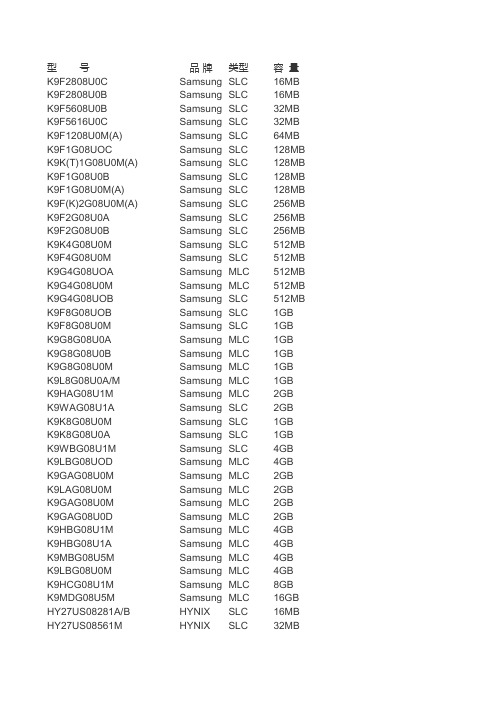
容量 16MB 16MB 32MB 32MB 64MB 128MB 128MB 128MB 128MB 256MB 256MB 256MB 512MB 512MB 512MB 512MB 512MB 1GB 1GB 1GB 1GB 1GB 1GB 2GB 2GB 1GB 1GB 4GB 4GB 2GB 2GB 2GB 2GB 4GB 4GB 4GB 4GB 8GB 16GB 16MB 32MB
MLC SLC MLC SLC SLC MLC MLC MLC SLC SLC MLC MLC MLC MLC MLC MLC MLC MLC MLC MLC MLC
技嘉主板支持CPU列表

GA-8I945PLGE-RH CPU支持列表主板型号GA-8I945PLGE-RH PCB 版本1.xCPU 广商CPU 型号外频800Intel Core™ 2 Extreme QX9770(C1,Yorkfield,45nm,3.2GHz,12 MB) 1600 - Intel Core™ 2 Extreme QX9770(C0,Yorkfield,45nm,3.2GHz,12 MB) 1600 - Intel Core™ 2 Extreme QX9650(C1,Yo rkfield,45nm,3GHz,12 MB) 1333 - Intel Core™ 2 Extreme QX9650(C0,Yorkfield,45nm,3GHz,12 MB) 1333 - Intel Core™ 2 Quad Q9650(E0,Yorkfield,45nm,3.0 GHz,12MB) 1333 - Intel Core™ 2 Quad Q9550(E0,Yorkfield,45nm,2.83GHz,12MB) 1333 - Intel Core™ 2 Quad Q9550(C1,Yorkfield,45nm,2.83GHz,12MB) 1333 - Intel Core™ 2 Quad Q9450(C1,Yorkfield,45nm,2.66GHz,12MB) 1333 - Intel Core™ 2 Quad Q9400(R0,Yorkfield,45nm,2.66GHz,6MB) 1333 -Intel Core™ 2 Quad Q9300(M1,Yorkfield,45nm,2.50GHz,6MB) 1333 -Intel Core™ 2 Qu ad Q8200(M1,Yorkfield,45nm,2.33GHz,4MB) 1333 -Intel Core™ 2 Duo E8600(E0,Wolfdale,45nm,3.33GHz,6MB) 1333 -Intel Core™ 2 Duo E8500(C0,Wolfdale,45nm,3.16GHz,6MB) 1333 -Intel Core™ 2 Duo E8500(E0,Wolfdale,45nm,3.16GHz,6MB) 1333 -Intel Core™ 2 Duo E8400(C0,Wolfdale,45nm,3GHz,6MB) 1333 -Intel Core™ 2 Duo E8400(E0,Wolfdale,45nm,3GHz,6MB) 1333 -Intel Core™ 2 Duo E8300(C0,Wolfdale,45nm,2.83GHz,6MB) 1333 -Intel Core™ 2 Duo E8200(C0,Wolfdale,45nm,2.66GHz,6MB) 1333 -Intel Core™ 2 Duo E8190(C0,W olfdale,45nm,2.66GHz,6MB) 1333 -Intel Core™ 2 Extreme QX6850(G0,Kentsfield,65nm,3GHz,8MB) 1333 - Intel Core™ 2 Extreme QX6800(G0,Kentsfield,65nm,2.93GHz,8MB) 1066 - Intel Core™ 2 Extreme QX6700(B3,Kentsfield,65nm,2.66GHz,8MB) 1066 - Intel Core™ 2 Extreme X6800(B2,Conroe XE,65nm,2.93GHz,4MB) 1066 - Intel Core™ 2 Quad Q6700(G0,Kentsfield,65nm,2.66GHz,8MB) 1066 - Intel Core™ 2 Quad Q6600(G0,Kentsfield,65nm,2.40HGz,8MB) 1066 - Intel Core™ 2 Quad Q6600(B3,Kentsfield,65nm,2.40GHz,8MB) 1066 - Intel Core™ 2 Duo E7500(M0,Wolfdale,45nm,2.93GHz,3MB) 1066 -Intel Core™ 2 Duo E7400(R0,Wolfdale,45nm,2.8GHz,3MB) 1066 -Intel Core™ 2 Duo E7300(M0,Wolfdale,45nm,2.66GHz,3MB) 1066 -Intel Core™ 2 Duo E7200(M0,Wolfdale,45nm,2.53GHz,3MB) 1066 -Intel Cor e™ 2 Duo E6850(G0,Conroe,65nm,3GHz,4MB) 1333 -Intel Core™ 2 Duo E6750(G0,Conroe,65nm,2.66GHz,4MB) 1333 -Intel Core™ 2 Duo E6700(B2,Conroe,65nm,2.66GHz,4MB) 1066 -Intel Core™ 2 Duo E6600(B2,Conroe,65nm,2.40GHz,4MB) 1066 -Intel Core™ 2 Duo E6550(G0,Conroe,65nm,2.33GHz,4MB) 1333 -Intel Core™ 2 Duo E6540(G0,Conroe,65nm,2.33GHz,4MB) 1333 -Intel Core™ 2 Duo E6420(B2,Conroe,65nm,2.13GHz,4MB) 1066 -Intel Core™ 2 Duo E6400(L2,Conroe,65nm,2.13GHz,2MB) 1066 -Intel Core™ 2 Duo E6400(B2,Conroe,65nm,2.13GHz,2MB) 1066 -Intel Core™ 2 Duo E6320(B2,Conroe,65nm,1.86GHz,4MB) 1066 -Intel Core™ 2 Duo E6300(L2,Conroe,65nm,1.86GHz,2MB) 1066 -Intel Core™ 2 Duo E6300(B2,Conroe,65nm,1.86GHz,2MB) 1066 -Intel Core™ 2 Duo E4700(G0,Conroe,65nm,2.60GHz,2MB) 800 -Intel Core™ 2 Duo E4600(M0,Conroe,65nm,2.40GH,2MB) 800 -Intel Core™ 2 Duo E4500(M0,Conroe,65nm,2.20GHz,2MB) 800 -Intel Core™ 2 Duo E4400(M0,Conroe,65nm,2GHz,2MB) 800 -Intel Core™ 2 Duo E4400(L2,Conroe,65nm,2GHz,2MB) 800 -Intel Core™ 2 Duo E4300(L2,Conroe,65nm,1.80GHz,2MB) 800 -Intel Pentium Dual-Core E5200(M0,Wolfdale,45nm,2.50GHz,2MB) 800 -Intel Pentium Dual-Core E2220(M0,Conroe,65nm,2.40GHz,1MB) 800 -Intel Pentium Dual-Core E2200(M0,Conroe,65nm,2.2GHz,1MB) 800 -Intel Pentium Dual-Core E2180(M0,Conroe,65nm,2.0GHz,1MB) 800 -Intel Pentium Dual-Core E2160(M0,Conroe,65nm,1.8GHz,1MB) 800 -Intel Pentium Dual-Core E2160(L2,Conroe,65nm,1.8GHz,1MB) 800 -Intel Pentium Dual-Core E2140(M0,Conroe,65nm,1.6GHz,1MB) 800 -Intel Pentium Dual-Core E2140(L2,Conroe,65nm,1.6GHz,1MB) 800 -Intel Celeron Dual-Core E1400(M0,Conroe,65nm,2.0GHz,512KB) 800 -Intel Celeron Dual-Core E1200(M0,Conroe,65nm,1.60GHz,512KB) 800 -Intel Pentium Extreme Edition 965(C1,Presler,65nm,3.73GHz,4MB) 1066 -Intel Pentium Extreme Edition 955(B1,Presler,65nm,3.46GHz,4MB (2x2)) 1066 - Intel Pentium Extreme Edition 840-XE(A0,Smithfield,90nm,3.20GHz,2MB) 800 - Intel Pentium D 960(D0,Presler,65nm,3.60GHz,4MB) 800 -Intel Pentium D 960(C1,Presler,65nm,3.60GHz,4MB (2x2)) 800 -Intel Pentium D 950(B1,Presler,65nm,3.40GHz,4MB (2x2)) 800 -Intel Pentium D 945(D0,Presler,65nm,3.40GHz,4MB) 800 -Intel Pentium D 945(C1,Presler,65nm,3.40GHz,4MB) 800 -Intel Pentium D 940(C1,Presler,65nm,3.20GHz,4MB) 800 -Intel Pentium D 940(B1,Presler,65nm,3.20GHz,4MB (2x2)) 800 -Intel Pentium D 935(D0,Presler,65nm,3.20GHz,4MB) 800 -Intel Pentium D 930(C1,Presler,65nm,3GHz,4MB) 800 -Intel Pentium D 930(B1,Presler,65nm,3GHz,4MB (2x2)) 800 -Intel Pentium D 925(C1,Presler,65nm,3GHz,4MB) 800 -Intel Pentium D 920(B1,Presler,65nm,2.80GHz,4MB (2x2)) 800 -Intel Pentium D 915(C1,Presler,65nm,2.80GHz,4MB) 800 -Intel Pentium D 840(B0,Smithfield,90nm,3.20GHz,2MB) 800 -Intel Pentium D 840(A0,Smithfield,90nm,3.20GHz,2MB) 800 -Intel Pentium D 830(B0,Smithfield,90nm,3GHz,2MB) 800 -Intel Pentium D 830(A0,Smithfield,90nm,3GHz,2MB) 800 -Intel Pentium D 820(B0,Smithfield,90nm,2.80GHz,2MB) 800 -Intel Pentium D 820(A0,Smithfield,90nm,2.80GHz,2MB) 800 -Intel Pentium D 805(B0,Smithfield,90nm,2.66GHz,2MB) 533 -Intel P4-Extreme Edition(N0,Prescott,90nm,3.73GHz,2MB) 1066 -Intel P4-Extreme Edition(M0,Northwood,0.13 micron,3.46GHz,2MB) 1066 - Intel P4-Extreme Edition(M0,Northwood,0.13 micron,3.40GHz,2MB) 800 -Intel Pentium 4 672(R0,Prescott,90nm,3.80GHz,2MB) 800 -Intel Pentium 4 670(R0,Prescott,90nm,3.80GHz,2MB) 800 -Intel Pentium 4 670(N0,Prescott,90nm,3.80GHz,2MB) 800 -Intel Pentium 4 662(R0,Prescott,90nm,3.60GHz,2MB) 800 -Intel Pentium 4 661(B1,Cedar Mill,65nm,3.60GHz,2MB) 800 -Intel Pentium 4 660(N0,Prescott,90nm,3.60GHz,2MB) 800 -Intel Pentium 4 651(D0,Cedar Mill,65nm,3.40GHz,2MB) 800 -Intel Pentium 4 651(B1,Cedar Mill,65nm,3.40GHz,2MB) 800 -Intel Pentium 4 650(R0,Prescott,90nm,3.40GHz,2MB) 800 -Intel Pentium 4 650(N0,Prescott,90nm,3.40GHz,2MB) 800 -Intel Pentium 4 641(D0,Cedar Mill,65nm,3.20GHz,2MB) 800 -Intel Pentium 4 641(B1,Cedar Mill,65nm,3.20GHz,2MB) 800 -Intel Pentium 4 640(N0,Prescott,90nm,3.20GHz,2MB) 800 -Intel Pentium 4 631(D0,Cedar Mill,65nm,3GHz,2MB) 800 -Intel Pentium 4 631(B1,Cedar Mill,65nm,3GHz,2MB) 800 -Intel Pentium 4 630(N0,Prescott,90nm,3GHz,2MB) 800 -Intel Pentium 4 571(E0,Prescott,90nm,3.80GHz,1MB) 800 -Intel Pentium 4 570J(E0,Prescott,90nm,3.80GHz,1MB) 800 -Intel Pentium 4 561(E0,Prescott,90nm,3.60GHz,1MB) 800 -Intel Pentium 4 560(D0,Prescott,90nm,3.60GHz,1MB) 800 -Intel Pentium 4 560J(E0,Prescott,90nm,3.60GHz,1MB) 800 -Intel Pentium 4 551(G1,Prescott,90nm,3.40GHz,1MB) 800 -Intel Pentium 4 551(E0,Prescott,90nm,3.40GHz,1MB) 800 -Intel Pentium 4 550(E0,Prescott,90nm,3.40GHz,1MB) 800 -Intel Pentium 4 550J(E0,Prescott,90nm,3.40GHz,1MB) 800 -Intel Pentium 4 541(E0,Prescott,90nm,3.20GHz,1MB) 800 -Intel Pentium 4 540(E0,Prescott,90nm,3.20GHz,1MB) 800 -Intel Pentium 4 531(E0,Prescott,90nm,3.00GHz,1MB) 800 -Intel Pentium 4 530(D0,Prescott,90nm,3GHz,1MB) 800 -Intel Pentium 4 530J(E0,Prescott,90nm,3GHz,1MB) 800 -Intel Pentium 4 524(G1,Prescott,90nm,3.06GHz,1MB) 533 -Intel Pentium 4 521(E0,Prescott,90nm,2.80GHz,1MB) 800 -Intel Pentium 4 520(D0,Prescott,90nm,2.80GHz,1MB) 800 -Intel Pentium 4 519K(G1,Prescott,90nm,3.06GHz,1MB) 533 -Intel Pentium 4 516(G1,Prescott,90nm,2.93GHz,1MB) 533 -Intel Pentium 4 516(E0,Prescott,90nm,2.93GHz,1MB) 533 -Intel Pentium 4 506(E0,Prescott,90nm,2.66GHz,1MB) 533 -Intel Pentium 4 505J(E0,Prescott,90nm,2.66GHz,1MB) 533 -Intel Celeron 400 Sequence 440(A1,Conroe-L,65nm,2GHz,512KB) 800 - Intel Celeron 400 Sequence 430(A1,Conroe-L,65nm,1.8GHz,512KB) 800 - Intel Celeron 400 Sequence 420(A1,Conroe-L,65nm,1.60GHz,512KB) 800 - Intel Celeron D 365(D0,Cedar Mill,65nm,3.60GHz,512KB) 533 -Intel Celeron D 360(D0,Cedar Mill,65nm,3.46GHz,512KB) 533 -Intel Celeron D 356(C1,Cedar Mill,65nm,3.33GHz,512KB) 533 -Intel Celeron D 355(G1,Prescott,90nm,3.33GHz,256KB) 533 -Intel Celeron D 352(C1,Cedar Mill,65nm,3.20GHz,512KB) 533 - Intel Celeron D 351(E0,Prescott,90nm,3.20GHz,256KB) 533 - Intel Celeron D 346(E0,Prescott,90nm,3.06GHz,256KB) 533 - Intel Celeron D 345J(E0,Prescott,90nm,3.06GHz,256KB) 533 - Intel Celeron D 341(E0,Prescott,90nm,2.93GHz,256KB) 533 - Intel Celeron D 340J(E0,Prescott,90nm,2.93GHz,256KB) 533 - Intel Celeron D 336(E0,Prescott,90nm,2.80GHz,256KB) 533 - Intel Celeron D 335J(E0,Prescott,90nm,2.80GHz,256KB) 533 - Intel Celeron D 331(E0,Prescott,90nm,2.66GHz,256KB) 533 - Intel Celeron D 330J(E0,Prescott,90nm,2.66GHz,256KB) 533 - Intel Celeron D 326(E0,Prescott,90nm,2.53GHz,256KB) 533 - Intel Celeron D 325J(E0,Prescott,90nm,2.53GHz,256KB) 533 - Intel Core™ 2 Extreme QX9770(3.2GHz,12 MB) 1600 N/AIntel Core™ 2 Extreme QX9650(3.0GHz,12MB) 1333 N/AIntel Core™ 2 Quad Q9650(3.0 GHz,12MB) 1333 N/AIntel Core™ 2 Quad Q9550(2.83GHz,12MB) 1333 N/AIntel Core™ 2 Quad Q9450(2.66GHz,12MB) 1333 N/AIntel Core™ 2 Quad Q9400(2.66GHz,6MB) 1333 N/AIntel Core™ 2 Quad Q9300(2.50GHz,6MB) 1333 N/AIntel Core™ 2 Quad Q8200(2.33GHz,4MB) 1333 N/AIntel Core™ 2 Duo E8600(3.33GHz,6MB) 1333 N/AIntel Core™ 2 Duo E8500(3.16GHz,6MB) 1333 N/AIntel Core™ 2 Duo E8400(3GHz,6MB) 1333 N/AIntel Core™ 2 Duo E8300(2.83GHz,6MB) 1333 N/AIntel Core™ 2 Duo E8200(2.66GHz,6MB) 1333 N/AIntel Core™ 2 Duo E8190(2.66GHz,6MB) 1333 N/AIntel Core™ 2 Extreme QX6850(3.0GHz,8MB) 1333 N/AIntel Core™ 2 Extreme QX6800(2.93GHz,8MB) 1066 N/AIntel Core™ 2 Extreme QX6700(2.66GHz,8MB) 1066 N/AIntel Core™ 2 Quad Q6700(2.66MHz,8MB) 1066 N/AIntel Core™ 2 Quad Q6600(2.4GHz,8MB) 1066 N/AIntel Core™ 2 Extreme X6800(2.93GHz,4MB) 1066 N/AIntel Core™ 2 Duo E7500(2.93GHz,3M B) 1066 N/AIntel Core™ 2 Duo E7400(2.8GHz,3MB) 1066 N/AIntel Core™ 2 Duo E7300(2.66GHz,3MB) 1066 N/AIntel Core™ 2 Duo E7200(2.53GHz,3MB) 1066 N/AIntel Core™ 2 Duo E6850(3.0GHz,4MB) 1333 N/AIntel Core™ 2 Duo E6750(2.66GHz,4MB) 1333 N/AIntel Core™ 2 Duo E6550(2.33GHz,4MB) 1333 N/AIntel Core™ 2 Duo E6540(2.33GHz,4MB) 1333 N/AIntel Core™ 2 Duo E6700(2.66GHz,4MB) 1066 N/AIntel Core™ 2 Duo E6600(2.4GHz,4MB) 1066 N/AIntel Core™ 2 Duo E6420(2.13GHz,4MB) 1066 N/AIntel Core™ 2 Duo E6400(2.13GHz,2MB) 1066 N/AIntel Core™ 2 Duo E6320(1.86GHz,4MB) 1066 N/AIntel Core™ 2 Duo E6300(1.86GHz,2MB) 1066 N/AIntel Core™ 2 Duo E4700(2.60GHz,2MB) 800 N/AIntel Core™ 2 Duo E4600(2.40GHz,2MB) 800 N/AIntel Core™ 2 Duo E4500(2.2GHz,2MB) 800 N/AIntel Core™ 2 Duo E4400(2.0GHz,2MB) 800 N/AIntel Core™ 2 Duo E4300(1.8GHz,2MB) 800 N/AIntel Pentium Dual-Core E5200(2.50GHz,2MB) 800 N/AIntel Pentium Dual-Core E2220(2.40GHz,1MB) 800 N/AIntel Pentium Dual-Core E2200(2.2GHz,1MB) 800 N/AIntel Pentium Dual-Core E2180(2.00GHz,1MB) 800 N/AIntel Pentium Dual-Core E2160(1.8GHz,1MB) 800 N/AIntel Pentium Dual-Core E2140(1.6GHz,1MB) 800 N/AIntel Celeron Dual-Core E1400(2.0GHz,512KB) 800 N/A Intel Celeron Dual-Core E1200(1.60GHz,512KB) 800 N/A Intel Pentium-Extreme Edition 965(3.73GHz,4MB) 1066 N/A Intel Pentium-Extreme Edition 955(3.46GHz,4MB) 1066 N/A Intel Pentium-Extreme Edition 840-XE(3.2GHz,2MB) 800 N/A Intel Pentium D 960(3.6GHz,4MB) 800 F4Intel Pentium D 950(3.4GHz,4MB) 800 F2Intel Pentium D 945(3.4GHz,4MB) 800 F4Intel Pentium D 940(3.2GHz,4MB) 800 F2Intel Pentium D 935(3.2GHz,4MB) 800 F2Intel Pentium D 930(3.0GHz,4MB) 800 F2Intel Pentium D 925(3.0GHz,4MB) 800 F4Intel Pentium D 920(2.8GHz,4MB) 800 F2Intel Pentium D 915(2.8GHz,4MB) 800 F4Intel P4-Extreme Edition 3.73GHz(2MB) 1066 F2(Run at FSB 800 MHz)Intel P4-Extreme Edition 3.46GHz(2MB) 1066 F2(Run at FSB 800 MHz)Intel P4-Extreme Edition 3.4GHz(2MB) 800 F2Intel Pentium D 840(3.2GHz,2MB) 800 F2Intel Pentium D 830(3.0GHz,2MB) 800 F2Intel Pentium D 820(2.8GHz,2MB) 800 F2Intel Pentium D 805(2.66GHz,2MB) 533 F2Intel Pentium 4 672(3.8GHz,2MB) 800 F2Intel Pentium 4 670(3.8GHz,2MB) 800 F2Intel Pentium 4 662(3.6GHz,2MB) 800 F2Intel Pentium 4 661(3.6GHz,2MB) 800 F2Intel Pentium 4 660(3.6GHz,2MB) 800 F2Intel Pentium 4 651(3.4GHz,2MB) 800 F2Intel Pentium 4 650(3.4GHz,2MB) 800 F2Intel Pentium 4 641(3.2GHz,2MB) 800 F2Intel Pentium 4 640(3.2GHz,2MB) 800 F2Intel Pentium 4 631(3.0GHz,2MB) 800 F2Intel Pentium 4 630(3.0GHz,2MB) 800 F2Intel Pentium 4 571(3.8GHz,1MB) 800 F2Intel Pentium 4 570J(3.8GHz,1MB) 800 F2Intel Pentium 4 561(3.6GHz,1MB) 800 F2Intel Pentium 4 560(J)(3.6GHz,1MB) 800 F2Intel Pentium 4 551(3.4GHz,1MB) 800 F2Intel Pentium 4 550(J)(3.4GHz,1MB) 800 F2Intel Pentium 4 541(3.2GHz,1MB) 800 F2Intel Pentium 4 540(J)(3.2GHz,1MB) 800 F1Intel Pentium 4 531(3.0GHz,1MB) 800 F2Intel Pentium 4 530(J)(3.0GHz,1MB) 800 F2Intel Pentium 4 524(3.06GHz,1MB) 533 F4Intel Pentium 4 521(2.8GHz,1MB) 800 F2Intel Pentium 4 520(J)(2.8GHz,1MB) 800 F2Intel Pentium 4 519K(3.06GHz,1MB) 533 F2Intel Pentium 4 516(2.93GHz,1MB) 533 F2Intel Pentium 4 515(J)(2.93GHz,1MB) 533 F2Intel Pentium 4 511(2.8GHz,1MB) 533 F1Intel Pentium 4 510(J)(2.8GHz,1MB) 533 F1Intel Pentium 4 506(2.66GHz,1MB) 533 F2Intel Pentium 4 505(J)(2.66GHz,1MB) 533 F2Intel Celeron 400 Sequence (Conroe-L) 440(2.0GHz,512KB) 800 N/A Intel Celeron 400 Sequence (Conroe-L) 430(1.8GHz,512KB) 800 N/A Intel Celeron 400 Sequence (Conroe-L) 420(1.6GHz,512KB) 800 N/A Intel Celeron D 360(3.46GHz,512KB) 533 F4Intel Celeron D 356(3.33GHz,512KB) 533 F4Intel Celeron D 355(3.33GHz,256KB) 533 F2Intel Celeron D 352(3.2GHz,512KB) 533 F4Intel Celeron D 351(3.2GHz,256KB) 533 F2Intel Celeron D 347(3.06GHz,512KB) 533 F4Intel Celeron D 346(3.06GHz,256KB) 533 F1Intel Celeron D 345J(3.06GHz,256KB) 533 F2Intel Celeron D 341(2.93GHz,256KB) 533 F1Intel Celeron D 340J(2.93GHz,256KB) 533 F2Intel Celeron D 336(2.8GHz,256KB) 533 F2Intel Celeron D 335J(2.8GHz,256KB) 533 F2Intel Celeron D 331(2.66GHz,256KB) 533 F2Intel Celeron D 330J(2.66GHz,256KB) 533 F2Intel Celeron D 326(2.53GHz,256KB) 533 F1Intel Celeron D 325J(2.53GHz,256KB) 533 F1。
- 1、下载文档前请自行甄别文档内容的完整性,平台不提供额外的编辑、内容补充、找答案等附加服务。
- 2、"仅部分预览"的文档,不可在线预览部分如存在完整性等问题,可反馈申请退款(可完整预览的文档不适用该条件!)。
- 3、如文档侵犯您的权益,请联系客服反馈,我们会尽快为您处理(人工客服工作时间:9:00-18:30)。
Draft Date
May. 15th 2001 Sep. 20th 2001
Remark
Advance
0.2
Nov. 5th 2001
Feb. 15th 2002
0.4
Apr. 15th 2002
Note : For more detailed features and specifications including FAQ, please refer to Samsung’s Flash web site. /Memory/Flash/datasheets.html The attached datasheets are prepared and approved by SAMSUNG Electronics. SAMSUNG Electronics CO., LTD. reserve the right to change the specifications. SAMSUNG Electronics will evaluate and reply to your requests and questions about device. If you have any questions, please contact the SAMSUNG branch office nply - 1.8V device(K9F56XXQ0B) : 1.65~1.95V - 3.3V device(K9F56XXU0B) : 2.7 ~ 3.6 V • Organization - Memory Cell Array - X8 device(K9F5608X0B) : (32M + 1024K)bit x 8 bit - X16 device(K9F5616X0B) : (16M + 512K)bit x 16bit - Data Register - X8 device(K9F5608X0B) : (512 + 16)bit x 8bit - X16 device(K9F5616X0B) : (256 + 8)bit x16bit • Automatic Program and Erase - Page Program - X8 device(K9F5608X0B) : (512 + 16)Byte - X16 device(K9F5616X0B) : (256 + 8)Word - Block Erase : - X8 device(K9F5608X0B) : (16K + 512)Byte - X16 device(K9F5616X0B) : ( 8K + 256)Word • Page Read Operation - Page Size - X8 device(K9F5608X0B) : (512 + 16)Byte - X16 device(K9F5616X0B) : (256 + 8)Word - Random Access : 10µs(Max.) - Serial Page Access : 50ns(Min.) • Fast Write Cycle Time - Program time : 200µs(Typ.) - Block Erase Time : 2ms(Typ.) • Command/Address/Data Multiplexed I/O Port • Hardware Data Protection - Program/Erase Lockout During Power Transitions • Reliable CMOS Floating-Gate Technology - Endurance : 100K Program/Erase Cycles - Data Retention : 10 Years • Command Register Operation • Intelligent Copy-Back • Unique ID for Copyright Protection • Package - K9F56XXU0B-YCB0/YIB0 48 - Pin TSOP I (12 x 20 / 0.5 mm pitch) - K9F56XXX0B-DCB0/DIB0 63- Ball TBGA ( 9 x 11 /0.8mm pitch , Width 1.0 mm) - K9F5608U0B-VCB0/VIB0 48 - Pin WSOP I (12X17X0.7mm) * K9F5608U0B-V(WSOPI ) is the same device as K9F5608U0B-Y(TSOP1) except package type.
1
K9F5608Q0B-DCB0,DIB0 K9F5608U0B-YCB0,YIB0 K9F5608U0B-DCB0,DIB0
K9F5616Q0B-DCB0,DIB0 K9F5616U0B-YCB0,YIB0 K9F5616U0B-DCB0,DIB0 K9F5608U0B-VCB0,VIB0
FLASH MEMORY
Document Title
32M x 8 Bit , 16M x 16 Bit NAND Flash Memory
Revision History
Revision No. History
0.0 0.1 Initial issue. At Read2 operation in X16 device : A3 ~ A7 are Don’t care ==> A3 ~ A 7 are "L" 1. IOL (R/B) of 1.8V device is changed. -min. Value: 7mA -->3mA -typ. Value: 8mA -->4mA 2. AC parameter is changed. tRP(min.) : 30ns --> 25ns 3. WP pin provides hardware protection and is recommended to be kept at V IL during power-up and power-down and recovery time of minimum 1µs is required before internal circuit gets ready for any command sequences as shown in Figure 15. ---> WP pin provides hardware protection and is recommended to be kept at VIL during power-up and power-down and recovery time of minimum 10µs is required before internal circuit gets ready for any command sequences as shown in Figure 15. 0.3 1. X16 TSOP1 pin is changed. : #36 pin is changed from VccQ to N.C . 1. In X16 device, bad block information location is changed from 256th byte to 256th and 261th byte. 2. tAR1, tAR2 are merged to tAR.(page 12) (before revision) min. tAR1 = 20ns , min. tAR2 = 50ns (after revision) min. tAR = 10ns 3. min. tCLR is changed from 50ns to 10ns.(page12) 4. min. tREA is changed from 35ns to 30ns.(page12) 5. min. tWC is changed from 50ns to 45ns.(page12) 6. Unique ID for Copyright Protection is available -The device includes one block sized OTP(One Time Programmable), which can be used to increase system security or to provide identification capabilities. Detailed information can be obtained by contact with Samsung. 7. tRHZ is divide into tRHZ and tOH.(page 12) - tRHZ : RE High to Output Hi-Z - tOH : RE High to Output Hold 8. tCHZ is divide into tCHZ and tOH.(page 12) - tCHZ : CE High to Output Hi-Z - tOH : CE High to Output Hold
32M x 8 Bit / 16M x 16 Bit NAND Flash Memory
PRODUCT LIST
Part Number K9F5608Q0B-D K9F5616Q0B-D K9F5608U0B-Y K9F5608U0B-D K9F5608U0B-V K9F5616U0B-Y K9F5616U0B-D 2.7 ~ 3.6V X16 X8 Vcc Range 1.65 ~ 1.95V Organization X8 X16 TSOP1 TBGA WSOP1 TSOP1 TBGA PKG Type TBGA
GENERAL DESCRIPTION
Offered in 32Mx8bit or 16Mx16bit, the K9F56XXX0B is 256M bit with spare 8M bit capacity. The device is offered in 1.8V or 3.3V Vcc. Its NAND cell provides the most cost-effective solutIon for the solid state mass storage market. A program operation can be performed in typical 200µs on the 528-byte(X8 device) or 264-word(X16 device) page and an erase operation can be performed in typical 2ms on a 16K-byte(X8 device) or 8K-word(X16 device) block. Data in the page can be read out at 50ns cycle time per word . The I/O pins serve as the ports for address and data input/output as well as command input. The on-chip write control automate s all program and erase functions including pulse repetition, where required, and internal verification and margining of data. Even the write-intensive systems can take advantage of the K9F56XXX0B′s extended reliability of 100K program/erase cycles by providing ECC(Error Correcting Code) with real time mapping-out algorithm. The K9F56XXX0B is an optimum solution for large nonvolatile storage applications such as solid state file storage and other port able applications requiring non-volatility.