WM8729
WM8725_Natertech
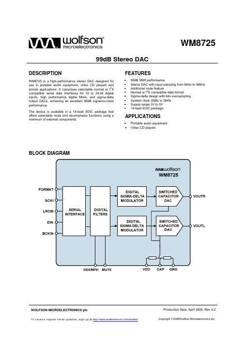
wWM872599dB Stereo DACWOLFSON MICROELECTRONICS plcProduction Data, April 2008, Rev 4.2DESCRIPTIONWM8725 is a high-performance stereo DAC designed for use in portable audio equipment, video CD players andsimilar applications. It comprises selectable normal or I 2S compatible serial data interfaces for 16 to 24-bit digital inputs, high performance digital filters, and sigma-delta output DACs, achieving an excellent 99dB signal-to-noise performance.The device is available in a 14-lead SOIC package that offers selectable mute and de-emphasis functions using a minimum of external components.FEATURES• 99dB SNR performance• Stereo DAC with input sampling from 8kHz to 96kHz • Additional mute feature• Normal or I 2S compatible data format• Sigma-delta design with 64x oversampling • System clock 256fs or 384fs • Supply range 3V to 5V • 14-lead SOIC packageAPPLICATIONS• Portable audio equipment •Video CD playersBLOCK DIAGRAMTABLE OF CONTENTS DESCRIPTION (1)FEATURES (1)APPLICATIONS (1)BLOCK DIAGRAM (1)TABLE OF CONTENTS (2)PIN CONFIGURATION (3)ORDERING INFORMATION (3)ABSOLUTE MAXIMUM RATINGS (4)RECOMMENDED OPERATING CONDITIONS (4)ELECTRICAL CHARACTERISTICS (5)PIN DESCRIPTION (6)INTERNAL POWER ON RESET (6)DEVICE DESCRIPTION (8)INTRODUCTION (8)DAC CIRCUITS (8)SERIAL DATA INTERFACE (9)SYSTEM CLOCK (10)RECOMMENDED EXTERNAL COMPONENTS (11)DETAIL OF RECOMMENDED EXTERNAL COMPONENTS SHOWING THE EXTERNAL LOW PASS FILTER (11)PCB LAYOUT (11)PACKAGE DIMENSIONS (12)ADDRESS: (13)w PD Rev 4.1 August 2004wPD Rev 4.1 August 2004PIN CONFIGURATIONVDDVOUTL MUTE NC DEEMPH SCKI FORMAT GNDVOUTR CAP NC BCKINLRCIN DINORDERING INFORMATIONDEVICE TEMPERATURE RANGE PACKAGE MOISTURE SENSITIVITY LEVEL PEAK BODYTEMPERATURE WM8725GED/V -25oC to +85oC14-lead SOIC (lead free) MSL2 260o C WM8725GED/RV-25o C to +85o C14-lead SOIC(Pb-free, tape and reel)MSL2 260o CNote:Reel quantity: 3,000wPD Rev 4.1 August 2004ABSOLUTE MAXIMUM RATINGSAbsolute Maximum Ratings are stress ratings only. Permanent damage to the device may be caused by continuously operating at or beyond these limits. Device functional operating limits and guaranteed performance specifications are given underElectrical Characteristics at the test conditions specified.ESD Sensitive Device. This device is manufactured on a CMOS process. It is therefore generically susceptible to damage from excessive static voltages. Proper ESD precautions must be taken during handling and storage of this device.Wolfson tests its package types according to IPC/JEDEC J-STD-020B for Moisture Sensitivity to determine acceptable storage conditions prior to surface mount assembly. These levels are:MSL1 = unlimited floor life at <30°C / 85% Relative Humidity. Not normally stored in moisture barrier bag. MSL2 = out of bag storage for 1 year at <30°C / 60% Relative Humidity. Supplied in moisture barrier bag. MSL3 = out of bag storage for 168 hours at <30°C / 60% Relative Humidity. Supplied in moisture barrier bag. The Moisture Sensitivity Level for each package type is specified in Ordering Information.CONDITION MIN MAXSupply voltage -0.3V +7.0V Reference inputVCC+0.3V Operating temperature range, T A -25oC +85oC Storage temperature-65oC +150oC Lead temperature (soldering, 10 seconds) +240oC Lead temperature (soldering, 2 minutes)+183o CRECOMMENDED OPERATING CONDITIONSPARAMETER SYMBOL TEST CONDITIONSMIN TYP MAX UNITSupply Range VDD -10% 3.0 to 5.0+10% V Ground GND 0 VVDD = 5V 15 25 mA Supply CurrentVDD = 3V7.5mAwPD Rev 4.1 August 2004ELECTRICAL CHARACTERISTICSTest ConditionsV DD = 5V, GND = 0V, T A = +25oC, fs = 48kHz, SCKI = 256fs unless otherwise stated.PARAMETER SYMBOL TEST CONDITIONS MIN TYP MAX UNITDigital Logic LevelsInput LOW level V IL 0.8 V Input HIGH levelV IH2.0 VAnalogue Output LevelsTo midrail or AC coupled(5V supply) 1 k Ω Load ResistanceTo midrail or AC coupled(3V supply)1 k Ω Maximum capacitance load 5V or 3V100pFOutput DC levelV DD /2 VReference LevelsPotential divider resistance V DD to CAP and CAP to GND 80 100 120 k ΩVoltage at CAPVDD = 5V 2.3 2.5 2.7 VDAC Circuit SpecificationsSNR (Note 1) VDD = 5V90 99 dBVDD = 3V 97 dBFull scale output voltage Into 10kohm VDD = 5V, 0dB 0.9 1.0 1.1 V RMSInto 10kohm VDD = 3V, 0dB0.6V RMSTHD (Full scale) 0dB 0.01 0.02 % THD+N (Dynamic range) -60dB 92 dB Frequency response 0 20,000 Hz Transition band 20,000 Hz Out of band rejection -40 dB Channel Separation 90 dB Gain mismatch channel-to-channel ±1 ±5 %FSRAudio Data Input and System Clock Timing InformationBCKIN pulse cycle time t BCY 100 ns BCKIN pulse width high t BCH 50 ns BCKIN pulse width lowt BCL 50 ns BCKIN rising edge to LRCIN edge t BL 30 ns LRCIN rising edge to BCKIN rising edge t LB 30 ns DIN setup time t DS 30 ns DIN hold timet DH 30 ns System clock pulse width high t SCKIH 13 ns System clock pulse width low t SCKIL13 nsNotes: 1. Ratio of output level with 1kHz full scale input, to the output level with all zeros into the digital input, measured “A” weighted over a 20Hz to 20kHz bandwidth.2.All performance measurements done with 20kHz low pass filter. Failure to use such a filter will result in higherTHD+N and lower SNR and Dynamic Range readings than are found in the Electrical Characteristics. The low pass filter removes out of band noise; although it is not audible, it may affect dynamic specification values.wPD Rev 4.1 August 2004PIN DESCRIPTIONPIN NAME TYPEDESCRIPTION1 LRCIN Digital input Sample rate clock input2 DIN Digital input Serial data input 3BCKIN Digital inputBit clock input 4 NC No connect No internal connection 5 CAP Analogue output Analogue internal reference 6 VOUTRAnalogue outputRight channel DAC output 7 GND Supply 0V supply 8 VDD Supply Positive supply 9 VOUTL Analogue output Left channel DAC output10 MUTE Digital input Mute control, high = muted. Internal pull-down 11 NC No connect No internal connection12 DEEMPH Digital input De-emphasis select, high = de-emphasis ON. Internal pull-up 13 FORMAT Digital input Data input format select, low = normal, high = I 2S. Internal pull-up 14SCKIDigital inputSystem clock input (256fs or 384fs)INTERNAL POWER ON RESETThe WM8725 includes a n internal power-on reset circuit. This is shown in Figure 1.Thisreset circuit is used to reset the digital logic into a default state after power up.Figure 1 Internal Power on Reset CircuitThe timing of the power on reset is shown in Figure 2 The circuit monitors VDD and VMID (CAP pin) and asserts PORB low when VMID is below the minimum threshold Vpor. It is assumed that VMID will rise slower than VCC due to the capacitor on VMID.wPD Rev 4.1 August 2004Figure 2 Power on/off Reset TimingSYMBOL Min Typ Max Unit Vpor 0.85 1.0 1.2 V Vpor_off 2.25 2.5 2.75 VTable 1 Power On/Off Reset TimingAt power on, when VDD and VMID have been established, PORB is released and the WM8725 has been reset.At power down, PORB is asserted low whenever VMID drops below the minimum threshold of Vpor_off.If VDD is removed at any time, the internal power-on reset circuit is powered down and PORB will follow VDD.DEVICE DESCRIPTIONINTRODUCTIONWM8725 is a complete stereo audio 16-24 bit digital-to-analogue converter, including digitalinterpolation filter, multibit sigma-delta with dither, and switched capacitor multibit stereoDAC and output smoothing filters.Special functions of mute and de-emphasis are provided, and operation using system clockof 256fs or 384fs is provided, selection between either clock rate being automaticallycontrolled. Sample rates (fs) from less than 8ks/s to 96ks/s are allowed, provided theappropriate system clock is input.MUTE DESCRIPTION0 Mute is OFF1 Mute is ONTable 2 Mute ControlA novel multi bit sigma-delta DAC design is used, utilising a 64x oversampling rate, tooptimise signal to noise performance and offer increased clock jitter tolerance.Internally generated midrail references are used to DC bias output signals, requiring only asingle external capacitor for decoupling purposes.Single 3V to 5V supplies may be used, the output amplitude scaling with absolute supplylevel. Low supply voltage operation and low current consumption, and the low pin count smallpackage, make the WM8725 attractive for many consumer type applications.DAC CIRCUITSThe WM8725 DACs are designed to allow playback of 16-bit PCM audio or similar data withhigh resolution and low noise and distortion. Sample rates up to 96ks/s may be used, withmuch lower sample rates acceptable provided that the ratio of sample rate (LRCIN) tosystem clock is maintained at the required 256fs or 384fs times.The DACs on WM8725 are implemented using sigma-delta oversampled conversiontechniques. These require that the PCM samples are digitally filtered and interpolated togenerate a set of samples at a much higher rate than the 96ks/s input rate. This samplestream is then digitally modulated to generate a digital pulse stream that is then converted toanalogue signals in a switched capacitor DAC. The advantage of this technique is that theDAC is linearised using noise shaping techniques, allowing the full performance to be metusing non-critical analogue components. A further advantage is that the high sample rate atthe DAC output means that smoothing filters on the output of the DAC need only have fairlycrude characteristics in order to remove the characteristic steps, or images, on the output ofthe DAC. To ensure that generation of tones characteristic to sigma-delta convertors is not aproblem, dithering is used in the digital modulator and a higher order modulator is used. Theswitched capacitor technique used in the DAC reduces sensitivity to clock jitter compared toswitched current techniques used in other implementations.De-emphasis of 44.1kHz signals may be applied if required.DEEMPH DESCRIPTION0 De-emphasis is OFF1 De-emphasis is ONTable 3 De-emphasis ControlThe voltage on the CAP pin is used as the reference for the DACs, therefore the amplitude ofthe signals at the DAC outputs will scale with the amplitude of the voltage at the CAP. Anexternal reference could be used to drive into the CAP pin if desired, but a value typically ofabout midrail should be used for optimum performance.w PD Rev 4.1 August 2004The outputs of the 2 DACs are buffered out of the device by buffer amplifiers. Theseamplifiers will source load current of several mA and sink current up to 1.5mA, so allowingsignificant loads to be driven. The output source is active and the sink is Class A, i.e. fixedvalue, so greater loads might be driven if an external ‘pull-down’ resistor is connected at theoutput.Typically an external low pass filter circuit will be used to remove residual sampling noise ofthe 64x oversampling used and if desired adjust the signal amplitude and device strength. SERIAL DATA INTERFACEWM8725 has serial interface formats that are fully compatible with both normal (MSB first, 16bit right-justified) and I2S interfaces. The data format is selected with the FORMAT pin. WhenFORMAT is LOW, normal data format is selected. When the format is HIGH, I2S format isselected. It must be noted that in “packed” mode operation (exactly 32 BCLKs per LRCINperiod), the data word must align exactly with LRCIN clock edges (effectively both left andright justified at the same time). This is true in both normal and I2S modes.FORMAT DESCRIPTION0 Normal format(MSB-first, 16 bit right justified)1 I2S format(Philips serial data protocol)Table 4 Serial Interface FormatsFigure 3 'Normal' Data Input TimingFigure 4 I2S Data Input Timingw PD Rev 4.1 August 2004wPD Rev 4.1 August 2004SYSTEM CLOCKThe system clock is used to operate the digital filters and the noise shaping circuits. The system clock input is at pin 14 (SCKI). The frequency of WM8725’s system clock should be set to 256fs or 384fs, (where fs is the audio sampling frequency). The sample rate is typically: 32 kHz, 44.1 kHz, 48 kHz or 96kHz.WM8725 has a system clock detection circuit that automatically determines whether the system clock being supplied is at 256fs or 384fs. The system clock should be synchronised with LRCIN, but WM8725 is tolerant of phase differences. Severe distortion in the phase difference between LRCIN and the system clock will be detected, and cause the device to automatically resynchronise. During resynchronisation, the output of the device will either repeat the previous sample, or drop the next sample, depending on the nature of the phase slip. This will ensure minimal “click“ at the analogue outputs during resynchronisation.Figure 5 System Clock Timing RequirementsSYSTEM CLOCK FREQUENCY(MHz)SAMPLING RATE (LRCIN)256fs 384fs 32 kHz 8.192 12.288 44.1 kHz 11.2896 16.9340 48 kHz12.28818.43296kHz 24.5761 36.8641Table 5 System Clock Frequencies Versus Sampling Rate Notes: 196kHz sample rate at either 256fs or 384fs are only supported with 5V supplies.Figure 6 Audio Data Input TimingRECOMMENDED EXTERNAL COMPONENTSFigure 7 Recommended External ComponentsDETAIL OF RECOMMENDED EXTERNAL COMPONENTS SHOWING THE EXTERNAL LOW PASS FILTERFigure 8 Third-Order Low Pass Filter (LPF) ExampleAn external low pass filter is recommended (see Figure 8) if the device is driving a widebandamplifier. In some applications, second-order or passive RC filter may be adequate.PCB LAYOUT1. Place all supply decoupling capacitors as close as possible to their respective supplypins and provide a low impedance path from the capacitors to the appropriate ground.2. Separate analogue and digital ground planes should be situated under respectiveanalogue and digital device pins.3. Avoid noise on the CAP reference pin. The decoupling capacitor should be placed asclose to this pin as possible with a low impedance path from the capacitor to analogueground.4. Digital input signals should be screened from each other and from other sources ofnoise to avoid cross-talk and interference. They should also run over the digital groundplane to avoid introducing unwanted noise into the analogue ground plane.5. Analogue output signal tracks should be kept as short as possible and over theanalogue ground plane reducing the possibility of losing signal quality.w PD Rev 4.1 August 2004wPD Rev 4.1 August 2004PACKAGE DIMENSIONSNOTES:A. ALL LINEAR DIMENSIONS ARE IN MILLIMETERS (INCHES).B. THIS DRAWING IS SUBJECT TO CHANGE WITHOUT NOTICE.C. BODY DIMENSIONS DO NOT INCLUDE MOLD FLASH OR PROTRUSION, NOT TO EXCEED 0.25MM (0.010IN).D. MEETS JEDEC.95 MS-012, VARIATION = AB. REFER TO THIS SPECIFICATION FOR FURTHER DETAILS.Symbols Dimensions(MM)Dimensions(Inches)MIN MAX MIN MAX A 1.35 1.750.05320.0688A10.100.250.00400.0098B 0.330.510.01300.0200C 0.190.250.00750.0098D 8.558.750.33670.3444E 3.80 4.000.14970.1574e 1.27 BSC 0.05 BSC H 5.80 6.200.22840.2440h 0.250.500.00990.0196L 0.40 1.270.01600.0500α0o 8o 0o 8oREF:JEDEC.95, MS-012IMPORTANT NOTICEWolfson Microelectronics plc (“Wolfson”) products and services are sold subject to Wolfson’s terms and conditions of sale, delivery and payment supplied at the time of order acknowledgement.Wolfson warrants performance of its products to the specifications in effect at the date of shipment. Wolfson reserves theright to make changes to its products and specifications or to discontinue any product or service without notice. Customers should therefore obtain the latest version of relevant information from Wolfson to verify that the information is current.Testing and other quality control techniques are utilised to the extent Wolfson deems necessary to support its warranty. Specific testing of all parameters of each device is not necessarily performed unless required by law or regulation.In order to minimise risks associated with customer applications, the customer must use adequate design and operating safeguards to minimise inherent or procedural hazards. Wolfson is not liable for applications assistance or customer product design. The customer is solely responsible for its selection and use of Wolfson products. Wolfson is not liable forsuch selection or use nor for use of any circuitry other than circuitry entirely embodied in a Wolfson product.Wolfson’s products are not intended for use in life support systems, appliances, nuclear systems or systems where malfunction can reasonably be expected to result in personal injury, death or severe property or environmental damage.Any use of products by the customer for such purposes is at the customer’s own risk.Wolfson does not grant any licence (express or implied) under any patent right, copyright, mask work right or other intellectual property right of Wolfson covering or relating to any combination, machine, or process in which its products or services might be or are used. Any provision or publication of any third party’s products or services does not constitute Wolfson’s approval, licence, warranty or endorsement thereof. Any third party trade marks contained in this document belong to the respective third party owner.Reproduction of information from Wolfson datasheets is permissible only if reproduction is without alteration and is accompanied by all associated copyright, proprietary and other notices (including this notice) and conditions. Wolfson isnot liable for any unauthorised alteration of such information or for any reliance placed thereon.Any representations made, warranties given, and/or liabilities accepted by any person which differ from those contained inthis datasheet or in Wolfson’s standard terms and conditions of sale, delivery and payment are made, given and/or accepted at that person’s own risk. Wolfson is not liable for any such representations, warranties or liabilities or for any reliance placed thereon by any person.ADDRESS:Wolfson Microelectronics plcWestfield House26 Westfield RoadEdinburghEH11 2QBUnited KingdomTel :: +44 (0)131 272 7000Fax :: +44 (0)131 272 7001Email :: sales@w PD Rev 4.1 August 2004。
Motorola 3.5 kHz 产品说明书
RVN4126 3.59100-386-9100-386/T DEVICERVN41772-CD2-3.5MCS/MTSRVN41821-CD2-3.5XTS3000/SABER PORTABLE YES RKN4046KHVN9085 3.51-20 R NO HLN9359 PROG. STAND RVN4057 3.532 X 8 CODEPLUG NO3080385B23 & 5880385B30 MDVN4965 3.59100-WS/T CONFIG KITRVN4053 3.5ASTRO DIGITAL INTERFACE NO3080385B23RVN41842-CD RKN4046A (Portable) 2-3.5ASTRO PORTABLE /MOBILE YES3080369B73 or0180300B10 (Mobile) RVN41831-CD3080369B732-3.5ASTRO SPECTRA MOBILE YES(Low / Mid Power)0180300B10 (High Power) RVN4185CD ASTRO SPECTRA PLUS MOBILE NO MANY OPTIONS; SEESERVICE BRIEF#SB-MO-0101RVN4186CD ASTRO SPECTRA PLUS MANY OPTIONS;MOBILE/PORTABLE COMB SEE SERVICE BRIEF#SB-MO-0101RVN4154 3.5ASTROTAC 3000 COMPAR.3080385B23RVN5003 3.5ASTROTAC COMPARATORS NO3080399E31 Adpt.5880385B34RVN4083 3.5BSC II NO FKN5836ARVN4171 3.5C200RVN4029 3.5CENTRACOM SERIES II NO VARIOUS-SEE MANUAL6881121E49RVN4112 3.5COMMAND PLUS NORVN4149 3.5COMTEGRA YES3082056X02HVN6053CD CT250, 450, 450LS YES AAPMKN4004RVN4079 3.5DESKTRAC CONVENTIONAL YES3080070N01RVN4093 3.5DESKTRAC TRUNKED YES3080070N01RVN4091 3.5DGT 9000 DESKSET YES0180358A22RVN4114 3.5GLOBAL POSITIONING SYS.NO RKN4021AHVN8177 3.5GM/GR300/GR500/GR400M10/M120/130YES3080070N01RVN4159 3.5GP60 SERIES YES PMLN4074AHVN9128 3.5GP300 & GP350RVN4152 3.5GP350 AVSRVN4150 3.5GTX YES HKN9857 (Portable)3080070N01(Mobile) HVN9025CD HT CDM/MTX/EX SERIES YES AARKN4083/AARKN4081RiblessAARKN4075RIBLESS NON-USA RKN4074RVN4098H 3.5HT1000/JT1000-VISAR YES3080371E46(VISAR CONV)RVN4151 3.5HT1000 AVSRVN4098 3.5HT1000/ VISAR CONV’L.YES RKN4035B (HT1000) HVN9084 3.5i750YES HLN-9102ARVN4156 3.5LCS/LTS 2000YES HKN9857(Portable)3080070N01(Mobile) RVN4087 3.5LORAN C LOC. RECV’R.NO RKN4021ARVN4135 3.5M100/M200,M110,M400,R100 includesHVN9173,9177,9646,9774YES3080070N01RVN4023 3.5MARATRAC YES3080070N01RVN4019 3.5MAXTRAC CONVENTIONAL YES3080070N01RVN4139 3.5MAXTRAC LS YES3080070N01RVN4043 3.5MAXTRAC TRK DUPLEX YES3080070N01RVN4178CD MC SERIES, MC2000/2500DDN6124AW/DB25 CONNECTORDDN6367AW/DB9 CONNECTOR RVN41751-CD Rib to MIC connector 1-3.5MCS2000 RKN4062BRVN41131-3.5MCS2000RVN4011 3.5MCX1000YES3000056M01RVN4063 3.5MCX1000 MARINE YES3000056M01RVN4117 3.5MDC/RDLAP DEVICESRVN4105 3.5MOBILE PROG. TOOLRVN4119 3.5MOBITEX DEVICESRVN4128 3.5MPT1327-1200 SERIES YES SEE MANUALRVN4025 3.5MSF5000/PURC/ANALOG YES0180355A30RVN4077 3.5MSF5000/10000FLD YES0180355A30RVN4017K 3.5MT 1000YES RTK4205CRVN4148 3.5MTR 2000YES3082056X02RVN4140 3.5MTRI 2000NORVN41761-CD MTS2000, MT2000*, MTX8000, MTX90001-3.5*programmed by DOS which is included in the RVN4176RVN4131 3.5MTVA CODE PLUG FIXRVN4142 3.5MTVA DOCTOR YES3080070N01RVN4131 3.5MTVA3.EXERVN4013 3.5MTX800 & MTX800S YES RTK4205CRVN4097 1-CD MTX8000/MTX9000,MTS2000,MT2000*,* programmed by DOS which is included in the RVN4176HVN9067CD MTX850/MTX8250MTX950,MTX925RVN4138 3.5MTX-LS YES RKN4035DRVN4035 3.5MX 1000YES RTK4203CRVN4073 3.5MX 800YES RKN4006BHVN9395 P100, P200 LB, P50+, P210, P500, PR3000RVN4134 3.5P100 (HVN9175)P200 LB (HVN9794)P50+ (HVN9395)P210 (HVN9763)P500 (HVN9941)PR3000 (HVN9586)YES RTK4205HVN9852 3.5P110YES HKN9755A/REX1143 HVN9262 3.5P200 UHF/VHF YES RTK4205RVN4129 3.5PDT220YVN4051 3.5PORTABLE REPEATER Portable rptr.P1820/P1821AXRVN4061C 3.5PP 1000/500NO3080385B23 & 5880385B30 RVN5002 3.5QUANTAR/QUANTRO NO3O80369E31RVN4135 3.5R100 (HVN9177)M100/M200/M110/M400YES0180358A52RVN4146 3.5RPM500/660RVN4002 3.5SABER YES RTK4203CRVN4131 3.5SETTLET.EXEHVN9007 3.5SM50 & SM120YESRVN4039 3.5SMART STATUS YES FKN5825AHVN9054 3.5SOFTWARE R03.2 P1225YES3080070N01HVN9001 3.5SOFTWARE R05.00.00 1225LS YES HLN9359AHVN9012 3.5SP50RVN4001N 3.5SPECTRA YES3080369B73 (STANDARD)0180300B10 (HIGH POWER) RVN4099 3.5SPECTRA RAILROAD YES3080369B73RVN4110 3.5STATION ACCESS MODULE NO3080369E31RVN4089A 3.5STX TRANSIT YES0180357A54RVN4051 3.5SYSTEMS SABER YES RTK4203BRVN4075 3.5T5600/T5620 SERIES NO3080385B23HVN9060CD TC3000, TS3000, TR3000RVN4123 3.5VISAR PRIVACY PLUS YES3080371E46FVN4333 3.5VRM 100 TOOLBOX FKN4486A CABLE &ADAPTORRVN4133 3.5VRM 500/600/650/850NORVN4181CD XTS 2500/5000 PORTABLES RKN4105A/RKN4106A RVN41002- 3.5XTS3000 ASTRO PORTABLE/MOBILERVN4170 3.5XTS3500YES RKN4035DRIB SET UPRLN4008E RADIO INTERFACE BOX (RIB)0180357A57RIB AC POWER PACK 120V0180358A56RIB AC POWER PACK 220V3080369B71IBM TO RIB CABLE (25 PIN) (USE WITH XT & PS2)3080369B72IBM TO RIB CABLE (9 PIN)RLN443825 PIN (F) TO 9 PIN (M) ADAPTOR (USE W/3080369B72 FOR AT APPLICATION) 5880385B308 PIN MODULAR TO 25 PIN ”D” ADAPTOR (FOR T5600 ONLY)0180359A29DUPLEX ADAPTOR (MOSTAR/TRAXAR TRNK’D ONLY)Item Disk Radio RIB Cable Number Size Product Required Number Item Disk Radio RIB Cable Number Size Product Required NumberUtilizing your personal computer, Radio Service Software (RSS)/Customer Programming Software (CPS)/CustomerConfiguration Software (CCS) enables you to add or reprogram features/parameters as your requirements change. RSS/CPS/CCS is compatible with IBM XT, AT, PS/2 models 30, 50, 60 and 80.Requires 640K RAM. DOS 3.1 or later. Consult the RSS users guide for the computer configuration and DOS requirements. (ForHT1000, MT/MTS2000, MTX838/8000/9000, Visar and some newer products —IBM model 386, 4 MEG RAM and DOS 5.0 or higher are recommended.) A Radio Interface Box (RIB) may be required as well as the appropriate cables. The RIB and cables must be ordered separately.Licensing:A license is required before a software (RVN) order is placed. The software license is site specific (customer number and ultimate destination tag). All sites/locations must purchase their own software.Be sure to place subsequent orders using the original customer number and ship-to-tag or other licensed sites; ordering software without a licensed customer number and ultimate tag may result in unnecessary delays. To obtain a no charge license agreement kit, order RPX4719. To place an order in the U.S. call 1-800-422-4210. Outside the U.S., FAX 847-576-3023.Subscription Program:The purchase of Radio ServiceSoftware/Customer Programming/Customer ConfigurationSoftware (RVN & HVN kits) entitles the buyer/subscriber to three years of free upgrades. At the end of these three years, the sub-scriber must purchase the same Radio Service Software kit to receive an additional three years of free upgrades. If the sub-scriber does not elect to purchase the same Radio Service Software kit, no upgrades will be sent. Annually a subscription status report is mailed to inform subscribers of the RSS/CPS/CCS items on our database and their expiration dates.Notes:1)A subscription service is offered on “RVN”-Radio Service Software/Customer Programming/Customer Configuration Software kits only.2)“RVN” software must only be procured through Radio Products and Services Division (RPSD). Software not procured through the RPSD will not be recorded on the subscription database; upgrades will not be mailed.3)Upgrades are mailed to the original buyer (customer number & ultimate tag).4)SP software is available through the radio product groups.The Motorola General Radio Service Software Agreement is now available on Motorola Online. If you need assistance please feel free to submit a “Contact Us” or call 800-422-4210.SMART RIB SET UPRLN1015D SMART RIB0180302E27 AC POWER PACK 120V 2580373E86 AC POWER PACK 220V3080390B49SMARTRIB CABLE (9 PIN (F) TO 9 PIN (M) (USE WITH AT)3080390B48SMARTRIB CABLE (25 PIN (F) TO 9 PIN (M) (USE WITH XT)RLN4488ASMART RIB BATTERY PACKWIRELESS DATA GROUP PRODUTS SOFTWARERVN4126 3.59100-386/9100T DEVICES MDVN4965 3.59100-WS/T CONFIG’TN RVN41173.5MDC/RDLAP DEVICESPAGING PRODUCTS MANUALS6881011B54 3.5ADVISOR6881029B90 3.5ADVISOR ELITE 6881023B20 3.5ADVISOR GOLD 6881020B35 3.5ADVISOR PRO FLX 6881032B30 3.5BR8506881032B30 3.5LS3506881032B30 3.5LS5506881032B30 3.5LS7506881033B10 3.5LS9506881035B20 3.5MINITOR III8262947A15 3.5PAGEWRITER 20008262947A15 3.5PAGEWRITER 2000X 6881028B10 3.5TALKABOUT T3406881029B35 3.5TIMEPORT P7308262947A15 3.5TIMEPORT P930NLN3548BUNIVERSAL INTERFACE KITItem Disk Radio NumberSize Product。
TI型号大全35-迈锐国际
TI型号⼤全35-迈锐国际ADC0820CCWMX/NOPB SOIC-201000EAR99TI迈锐国际胡浩亮137********ADC082S021CIMM/NOPB VSSOP-81000EAR99TI迈锐国际胡浩亮137********ADC082S021CIMMX/NOPB VSSOP-83500EAR99TI迈锐国际胡浩亮137********ADC082S051CIMM/NOPB VSSOP-81000EAR99TI迈锐国际胡浩亮137********ADC082S101CIMM/NOPB VSSOP-81000EAR99TI迈锐国际胡浩亮137********ADC082S101CIMMX/NOPB VSSOP-83500EAR99TI迈锐国际胡浩亮137********ADC083000CIYB/NOPB HLQFP-1286003A001A5A1TI迈锐国际胡浩亮137********ADC083000CIYB/S7002214HLQFP-1286003A001A5A1TI迈锐国际胡浩亮137********ADC0831CCN/NOPB PDIP-81000EAR99TI迈锐国际胡浩亮137********ADC0831CCWM/NOPB SOIC-143000EAR99TI迈锐国际胡浩亮137********ADC0831CCWMX/NOPB SOIC-141000EAR99TI迈锐国际胡浩亮137********ADC0832CCN/NOPB PDIP-81000EAR99TI迈锐国际胡浩亮137********ADC0832CCWM/NOPB SOIC-143000EAR99TI迈锐国际胡浩亮137********ADC0832CCWMX/NOPB SOIC-141000EAR99TI迈锐国际胡浩亮137********ADC0834CCN/NOPB PDIP-14500EAR99TI迈锐国际胡浩亮137********ADC0834CCWM/NOPB SOIC-143000EAR99TI迈锐国际胡浩亮137********ADC0834CCWMX/NOPB SOIC-141000EAR99TI迈锐国际胡浩亮137********ADC08351CILQE/NOPB WQFN-24250EAR99TI迈锐国际胡浩亮137********ADC08351CILQX/NOPB WQFN-244500EAR99TI迈锐国际胡浩亮137********ADC08351CIMTCE/NOPB TSSOP-20250EAR99TI迈锐国际胡浩亮137********ADC08351CIMTCX/NOPB TSSOP-202500EAR99TI迈锐国际胡浩亮137********ADC08351EVM RFIDSUB01EAR99TI迈锐国际胡浩亮137********ADC0838CCWM/NOPB SOIC-202160EAR99TI迈锐国际胡浩亮137********ADC0838CCWMX/NOPB SOIC-201000EAR99TI迈锐国际胡浩亮137********ADC0838CIWM/NOPB SOIC-202160EAR99TI迈锐国际胡浩亮137********ADC0838CIWMX/NOPB SOIC-201000EAR99TI迈锐国际胡浩亮137********ADC0848BCV/NOPB PLCC-281750EAR99TI迈锐国际胡浩亮137********ADC0848BCVX/NOPB PLCC-28750EAR99TI迈锐国际胡浩亮137********ADC0848CCV/NOPB PLCC-281750EAR99TI迈锐国际胡浩亮137******** ADC0848CCVX/NOPB PLCC-28750EAR99TI迈锐国际胡浩亮137********ADC084S021CIMM/J7001218VSSOP-101000EAR99TI迈锐国际胡浩亮137********ADC084S021CIMM/NOPB VSSOP-101000EAR99TI迈锐国际胡浩亮137********ADC084S021CIMMX/NOPB VSSOP-103500EAR99TI迈锐国际胡浩亮137********ADC084S051CIMM/NOPB VSSOP-101000EAR99TI迈锐国际胡浩亮137********ADC084S101CIMM/NOPB VSSOP-101000EAR99TI迈锐国际胡浩亮137********ADC08500CIYB/NOPB HLQFP-1286003A991C1TI迈锐国际胡浩亮137********ADC08831IM SOIC-89500EAR99TI迈锐国际胡浩亮137********ADC08831IM/NOPB SOIC-89500EAR99TI迈锐国际胡浩亮137********ADC08831IMX/NOPB SOIC-82500EAR99TI迈锐国际胡浩亮137********ADC08832IMM/NOPB VSSOP-81000EAR99TI迈锐国际胡浩亮137********ADC08832IM/NOPB SOIC-89500EAR99TI迈锐国际胡浩亮137********ADC08832IMX/NOPB SOIC-82500EAR99TI迈锐国际胡浩亮137********ADC088S022CIMT TSSOP-169200EAR99TI迈锐国际胡浩亮137********ADC088S022CIMT/NOPB TSSOP-169200EAR99TI迈锐国际胡浩亮137********ADC088S022CIMTX/NOPB TSSOP-162500EAR99TI迈锐国际胡浩亮137********ADC088S052CIMT/NOPB TSSOP-169200EAR99TI迈锐国际胡浩亮137********ADC088S052CIMTX/NOPB TSSOP-162500EAR99TI迈锐国际胡浩亮137********ADC088S102CIMT/NOPB TSSOP-169200EAR99TI迈锐国际胡浩亮137********ADC088S102CIMTX/NOPB TSSOP-162500EAR99TI迈锐国际胡浩亮137********ADC08B200CIVS/NOPB TQFP-482500EAR99TI迈锐国际胡浩亮137********ADC08B200QCIVS/NOPB TQFP-482500EAR99TI迈锐国际胡浩亮137********ADC08B3000CIYB/NOPB HLQFP-1286003A991C1TI迈锐国际胡浩亮137********ADC08B3000RB/NOPB RFIDSUB01EAR99TI迈锐国际胡浩亮137********ADC08D1000CIYB/NOPB HLQFP-1286003A001A5A1TI迈锐国际胡浩亮137********ADC08D1010DIYB/NOPB HLQFP-1286003A001A5A1TI迈锐国际胡浩亮137********ADC08D1020CIYB/NOPB HLQFP-1286003A001A5A1TI迈锐国际胡浩亮137********ADC08D1500CIYB/NOPB HLQFP-1286003A001A5A1TI迈锐国际胡浩亮137********ADC08D1520CIYB/NOPB HLQFP-1286003A001A5A1TI迈锐国际胡浩亮137********ADC08D1520CIYB/S7002396HLQFP-1286003A001A5A1TI迈锐国际胡浩亮137********ADC08D1520CVAL RFIDSUB013A002H1A TI迈锐国际胡浩亮137********迈锐国际胡浩亮ADC08D1520RB/NOPB RFIDSUB013A002H1A TI137******** ADC08D1520WGFQV CQFP-128243A001A2C TI迈锐国际胡浩亮137********ADC08D1520WGMPR CQFP-128243A001A5A1TI迈锐国际胡浩亮137********ADC08D500CIYB/NOPB HLQFP-1286003A991C1TI迈锐国际胡浩亮137********ADC08D500CIYB/S7002554HLQFP-1286003A991C1TI迈锐国际胡浩亮137********ADC08D500CIYB/S7002952HLQFP-1286003A991C1TI迈锐国际胡浩亮137********ADC08D502CIYB/NOPB HLQFP-1286003A991C1TI迈锐国际胡浩亮137********ADC08DJ3200AAV FCBGA-1448403A001A5A1TI迈锐国际胡浩亮137********ADC08DJ3200AAVT FCBGA-1442503A001A5A1TI迈锐国际胡浩亮137********ADC08DJ3200EVM UNKNOWN-14413A002H1A TI迈锐国际胡浩亮137********ADC08DL500CIVV/NOPB LQFP-1446003A991C1TI迈锐国际胡浩亮137********ADC08DL502CIVV/NOPB LQFP-1446003A991C1TI迈锐国际胡浩亮137********ADC08L060CIMT/NOPB TSSOP-246100EAR99TI迈锐国际胡浩亮137********ADC08L060CIMTX/NOPB TSSOP-242500EAR99TI迈锐国际胡浩亮137********ADC08L060EVM RFIDSUB01EAR99TI迈锐国际胡浩亮137********ADC09QJ1300EVM RFIDSUB01EAR99TI迈锐国际胡浩亮137********ADC10040CIMT/NOPB TSSOP-284800EAR99TI迈锐国际胡浩亮137********ADC10040CIMTX/NOPB TSSOP-282500EAR99TI迈锐国际胡浩亮137********ADC10040QCIMT/NOPB TSSOP-284800EAR99TI迈锐国际胡浩亮137********ADC10040QCIMTX/NOPB TSSOP-282500EAR99TI迈锐国际胡浩亮137********ADC10065CIMT/NOPB TSSOP-284800EAR99TI迈锐国际胡浩亮137********ADC10065CIMTX/NOPB TSSOP-282500EAR99TI迈锐国际胡浩亮137********ADC10080CIMT/NOPB TSSOP-284800EAR99TI迈锐国际胡浩亮137********ADC10080CIMTX/NOPB TSSOP-282500EAR99TI迈锐国际胡浩亮137********ADC101C021CIMK/NOPB SOT-23-THN-61000EAR99TI迈锐国际胡浩亮137********ADC101C021CIMKX/NOPB SOT-23-THN-63000EAR99TI迈锐国际胡浩亮137********ADC101C021CIMM/NOPB VSSOP-81000EAR99TI迈锐国际胡浩亮137********ADC101C027CIMK/NOPB SOT-23-THN-61000EAR99TI迈锐国际胡浩亮137********ADC101C027CIMKX/NOPB SOT-23-THN-63000EAR99TI迈锐国际胡浩亮137********ADC101S021CIMF/NOPB SOT-23-61000EAR99TI迈锐国际胡浩亮137********ADC101S021CIMFX/NOPB SOT-23-63000EAR99TI迈锐国际胡浩亮137********迈锐国际胡浩亮ADC101S021CISD/NOPB WSON-61000EAR99TI137********ADC101S021CISDX/NOPB WSON-64500EAR99TI迈锐国际胡浩亮137********ADC101S051CIMF/NOPB SOT-23-61000EAR99TI迈锐国际胡浩亮137********ADC101S051CIMFX/NOPB SOT-23-63000EAR99TI迈锐国际胡浩亮137********ADC101S051QIMF/NOPB SOT-23-61000EAR99TI迈锐国际胡浩亮137********ADC101S051QIMFX/NOPB SOT-23-63000EAR99TI迈锐国际胡浩亮137********ADC101S101CIMF/NOPB SOT-23-61000EAR99TI迈锐国际胡浩亮137********ADC101S101CIMFX/NOPB SOT-23-63000EAR99TI迈锐国际胡浩亮137********ADC101S101CISD/NOPB WSON-61000EAR99TI迈锐国际胡浩亮137********。
WM8728

FEATURES
• • Stereo DAC with 24 bit PCM or single bit DSD operation Audio Performance - 106dB SNR (‘A’ weighted @ 48kHz) DAC - -97dB THD DAC Sampling Frequency: 8kHz - 192kHz 2 or 3-Wire Serial Control Interface or Hardware Control Programmable Audio Data Interface Modes - I2S, Left, Right Justified, DSP - 16/20/24/32 bit Word Lengths Independent Digital Volume Control on Each Channel with 127.5dB Range in 0.5dB Steps 3.0V - 5.5V Supply Operation 20-pin SSOP Package Exceeds Dolby Class A Performance Requirements
SIGMA DELTA MODULATOR
MUX
LEFT DAC
LOW PASS FILTER
VOUTL
VMID
MCLK
AVDD DVDD
VREFP VREFN AGND
DGND
WOLFSON MICROELECTRONICS LTD
Lutton Court, Bernard Terrace, Edinburgh, EH8 9NX, UK Tel: +44 (0) 131 667 9386 Fax: +44 (0) 131 667 5176 Email: sales@
雷赛步进电机选型参考
步进电机的种类和特点步进电机在构造上有三种主要类型:反应式(Variable Reluctance,VR)、永磁式(Permanent Magnet,PM)和混合式(Hybrid Stepping,HS)。
*反应式定子上有绕组、转子由软磁材料组成。
结构简单、成本低、步距角小,可达1。
2°、但动态性能差、效率低、发热大,可靠性难保证。
*永磁式永磁式步进电机的转子用永磁材料制成,转子的极数与定子的极数相同。
其特点是动态性能好、输出力矩大,但这种电机精度差,步矩角大(一般为7。
5°或15°)。
*混合式混合式步进电机综合了反应式和永磁式的优点,其定子上有多相绕组、转子上采用永磁材料,转子和定子上均有多个小齿以提高步矩精度。
其特点是输出力矩大、动态性能好,步距角小,但结构复杂、成本相对较高。
按定子上绕组来分,共有二相、三相和五相等系列。
最受欢迎的是两相混合式步进电机,约占97%以上的市场份额,其原因是性价比高,配上细分驱动器后效果良好.该种电机的基本步距角为1。
8°/步,配上半步驱动器后,步距角减少为0。
9°,配上细分驱动器后其步距角可细分达256倍 (0.007°/微步).由于摩擦力和制造精度等原因,实际控制精度略低。
同一步进电机可配不同细分的驱动器以改变精度和效果。
雷赛步进电机系列雷赛两相、三相混合式步进电机,采用优质冷轧钢片和耐高温永磁体制造,产品规格涵盖35-130范围。
具有温升低、可靠性高的特点,由于其具有良好的内部阻尼特性,因而运行平稳,无明显震荡区。
可满足不同行业、不同环境下的使用需求。
雷赛采用专利技术研发的三相步进电机驱动系统,更好地解决了传统步进电机低速爬行、有共振区、噪音大、高速扭矩小、起动频率低和驱动器可靠性差等缺点,具有交流伺服电机的某些运行特性,其运行效果可与进口产品相媲美.两相步进电机命名规则<〉上例表示机座号为57mm,两相混合式,步距角为1.8度,扭矩0。
光纤转换模块光电转换器光纤链路模块光纤收发器

光纤转换模块光电转换器光纤链路模块光纤收发器modbus光纤中继器,光纤转换模块,光电转换器,光纤链路模块,光纤收发器,光端机,光传输北京西山军通科技有限公司张宏年136******** 157******** 010-******** QQ:489503206国产第一高性能现场总线产品,可替代进口产品。
现在用进口的,给你降低一些成本;现在用国产的,给你提高些档次。
坚持国产化,为民族企业谋福祉Schneider(施耐德);Modicon(莫迪康)MB+and S908 RIO中继器系列产品与NS23产品型号对照表NS23产品型号Modicon产品NS2304MT 490NRP25300 NS2304ST--NS2301MT 490NRP25400 NWFR85D200 NS2301ST--NS2314MT--NS2314ST--NS2311MT 490NRP95400 NWFR89D200 NS2311ST--NS2306RE NWRR85001(RR85 Repeater)Schneider(施耐德)、Modicon(莫迪康)MB+and S908 RIO的光产品种类比较少,且只有多模产品,我们的产品种类比他们多,比他们全。
专为现场总线ModbusPLUS(MB+)提供的光纤传输产品及通信解决方案-军通科技NS230 NS230系列产品是参考Modicon的Modbus PLUS系列光纤中继器产品的功能,采用多项最新技术研发而成的Modbus PLUS(MB+)总线光纤链路模块。
它可以完成通过光纤传输Modbus PLUS现场总线,在功能上可以代替490NRP25300,490NRP25400,490NRP95400,NWFR85D200等产品。
此产品具有的优点有:体积小、低功耗、工业级设计、电源适应性、优美的外观与导轨式安装机壳等等…,同时,还有如下几个突出的特点:金属铸造工艺外壳,特有的解环协议、型号丰富的系列化产品等。
MCP2517xFD CAN FD母板商品说明书
PIC32MX470F512H-120/PT Digi-Key
PIC32MX470F512H TQFP-64
U2
MCHP ANALOG LDO 3.3V MCP1826S- Microchip Technology
MCP1826S-3302E/DB
Microchip Technology
3302E/DB SOT-223-3
Bill of Materials
Document Number: 02-10615
Board Number:
04-10615
Part Number: Revision: Engineer: Drawn By:
ADM00576 4 Wilhelm Leichtfried Wilhelm Leichtfried
Digi-Key Digi-Key
Digi-Key
Digi-Key Digi-Key
Digi-Key Digi-Key
Digi-Key
Digi-Key Digi-Key Digi-Key
Microchip Parts listed below
U1
MCHP MCU 32-BIT 120MHz 512kB 128k Microchip Technology
02-10615-R4_BOM_Web.xls
Page 2
CON HDR-2.54 Male 1x1 Gold 5.84MH TH TE Connectivity
5-146280-1
VERT
CON HDR-2.54 Male 1x2 Tin 5.84MH TH Sullins Connector Solutions
PREC002SAAN-RC
众鑫微2017第二版图册
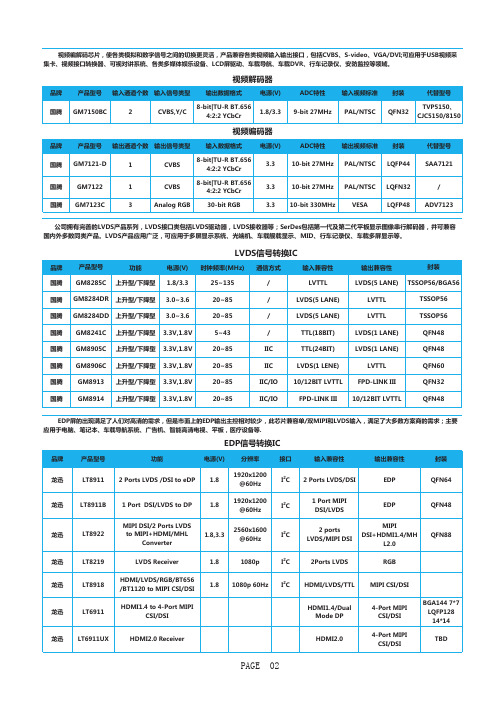
品牌功能电源(V)时钟频率(MHz)通信方式输入兼容性输出兼容性国腾上升型/下降型 1.8/3.325~135/LVTTL LVDS(5 LANE)国腾上升型/下降型 3.0~3.620~85/LVDS(5 LANE)LVTTL 国腾上升型/下降型 3.0~3.620~85/LVDS(5 LANE)LVTTL 国腾上升型/下降型 3.3V,1.8V 5~43/TTL(18BIT)LVDS(1 LANE)国腾上升型/下降型 3.3V,1.8V 20~85IIC TTL(24BIT)LVDS(1 LANE)国腾上升型/下降型 3.3V,1.8V 20~85IIC LVDS(1 LENE)LVTTL 国腾上升型/下降型 3.3V,1.8V 20~85IIC/IO 10/12BIT LVTTL FPD-LINK III 国腾上升型/下降型3.3V,1.8V20~85IIC/IOFPD-LINK III10/12BIT LVTTL公司拥有完善的LVDS 产品系列,LVDS 接口类包括LVDS 驱动器,LVDS 接收器等;SerDes 包括第一代及第二代平板显示图像串行解码器,并可兼容国内外多数同类产品。
LVDS 产品应用广泛,可应用于多屏显示系统、光端机、车载舰载显示、MID 、行车记录仪、车载多屏显示等。
LVDS 信号转换IC产品型号封装GM8285C TSSOP56/BGA56GM8284DR TSSOP56QFN48GM8284DD TSSOP56GM8241C QFN48GM8905C QFN48GM8906C QFN60GM8913QFN32GM8914品牌输出通道个数输出信号类型输入数据格式电源(V)ADC 特性输出视频标准封装代替型号国腾1CVBS 8-bit|TU-R BT.6564:2:2 YCbCr 3.310-bit 27MHz PAL/NTSC LQFP44SAA7121国腾1CVBS 8-bit|TU-R BT.6564:2:2 YCbCr3.310-bit 27MHz PAL/NTSC LQFN32/国腾3Analog RGB30-bit RGB3.310-bit 330MHzVESALQFP48ADV7123视频编解码芯片,使各类模拟和数字信号之间的切换更灵活,产品兼容各类视频输入输出接口,包括CVBS 、S-video 、VGA/DVI;可应用于USB 视频采集卡、视频接口转换器、可视对讲系统、各类多媒体娱乐设备、LCD 屏驱动、车载导航、车载DVR 、行车记录仪、安防监控等领域。
- 1、下载文档前请自行甄别文档内容的完整性,平台不提供额外的编辑、内容补充、找答案等附加服务。
- 2、"仅部分预览"的文档,不可在线预览部分如存在完整性等问题,可反馈申请退款(可完整预览的文档不适用该条件!)。
- 3、如文档侵犯您的权益,请联系客服反馈,我们会尽快为您处理(人工客服工作时间:9:00-18:30)。
ADDRESS: ........................................................................................................................18
w
PD Rev 4.1 June 2006 2
WM8729
FEATURES
• • Stereo DAC Audio Performance 106dB SNR (‘A’ weighted @ 48kHz) DAC -97dB THD DAC Sampling Frequency: 8kHz – 192kHz Pin Selectable Audio Data Interface Format I S or Right Justified 3.0V - 5.5V Supply Operation 16-lead SOIC Package Exceeds Dolby Class A Performance Requirements
WM8729
Production Data
TABLE OF CONTENTS
DESCRIPTION ............................................................................................................1 FEATURES..................................................................................................................1 APPLICATIONS ..........................................................................................................1 BLOCK DIAGRAM ......................................................................................................1 TABLE OF CONTENTS ..............................................................................................2 PIN CONFIGURATION................................................................................................3 ORDERING INFORMATION .......................................................................................3 PIN DESCRIPTION .....................................................................................................4 ABSOLUTE MAXIMUM RATINGS..............................................................................5 DC ELECTRICAL CHARACTERISTICS .....................................................................6 ELECTRICAL CHARACTERISTICS ...........................................................................6
To receive regular email updates, sign up at /enews/
Production Data, June 2006, Rev 4.1 Copyright 2006 Wolfson Microelectronics plc
RECOMMENDED ANALOGUE LOW PASS FILTER (OPTIONAL) .........................16 PACKAGE DRAWING...............................................................................................17 IMPORTANT NOTICE ...............................................................................................18
WM8729
Production Data
PIN CONFIGURATION
LRCIN DIN BCKIN MCLK DGND DVDD VOUTR AGND
1 ORMAT
DEM
MUTEB
WM8729
13 12 11 10 9
VREFP
VREFN
VMID VOUTL AVDD
w
24-bit, 192kHz Stereo DAC
DESCRIPTION
The WM8729 is a high performance stereo DAC designed for audio applications such as DVD, home theatre systems, and digital TV. The WM8729 supports data input word lengths from 16 to 24-bits and sampling rates up to 192kHz. The WM8729 consists of a serial interface port, digital interpolation filters, multi-bit sigma delta modulators and stereo DAC in a small 16-pin SOIC package. The WM8729 has a hardware control interface for selection of audio data interface format and de-emphasis. The WM8729 is an ideal device to interface to AC-3, DTS, and MPEG audio decoders for surround sound applications, or for use in DVD players, including supporting the implementation of 2 channels at 192kHz for high-end DVD-Audio applications.
2
• • • • •
APPLICATIONS
• • • • DVD-Audio and DVD ‘Universal’ Players Home theatre systems Digital TV Digital broadcast receivers
BLOCK DIAGRAM
WOLFSON MICROELECTRONICS plc
ORDERING INFORMATION
DIGITAL DE-EMPHASIS CHARACTERISTICS ........................................................14 APPLICATIONS INFORMATION ..............................................................................15
DEVICE DESCRIPTION..............................................................................................9
INTRODUCTION ................................................................................................................ 9 CLOCKING SCHEMES ...................................................................................................... 9 DIGITAL AUDIO INTERFACE ............................................................................................ 9 AUDIO DATA SAMPLING RATES.....................................................................................10 HARDWARE CONTROL MODES .....................................................................................11 DIGITAL FILTER CHARACTERISTICS.............................................................................13 DAC FILTER RESPONSES...............................................................................................13