四象限乘法器设计
四象限乘法器
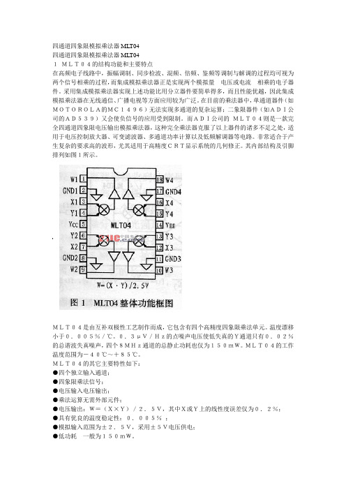
四通道四象限模拟乘法器MLT04四通道四象限模拟乘法器MLT041MLT04的结构功能和主要特点在高频电子线路中,振幅调制、同步检波、混频、倍频、鉴频等调制与解调的过程均可视为两个信号相乘的过程,而集成模拟乘法器正是实现两个模拟量电压或电流相乘的电子器件。
采用集成模拟乘法器实现上述功能比用分立器件要简单得多,而且性能优越,因此集成模拟乘法器在无线通信、广播电视等方面应用较为广泛。
在目前的乘法器中,单通道器件(如MOTOROLA的MC1496)无法实现多通道的复杂运算;二象限器件(如ADI公司的AD539)又会使负信号的应用受到限制。
而ADI公司的MLT04则是一款完全四通道四象限电压输出模拟乘法器,这种完全乘法器克服了以上器件的诸多不足之处,适用于电压控制放大器、可变滤波器、多通道功率计算以及低频解调器等电路。
非常适合于产生复杂的要求高的波形,尤其适用于高精度CRT显示系统的几何修正。
其内部结构及引脚排列如图1所示。
MLT04是由互补双极性工艺制作而成,它包含有四个高精度四象限乘法单元。
温度漂移小于0.005%/℃。
0.3μV/Hz的点噪声电压使低失真的Y通道只有0.02%的总谐波失真噪声,四个8MHz通道的总静止功耗也仅为150mW。
MLT04的工作温度范围为-40℃~+85℃。
MLT04的其它主要特性如下:●四个独立输入通道;●四象限乘法信号;●电压输入电压输出;●乘法运算无需外部元件;●电压输出:W=(X×Y)/2.5V,其中X或Y上的线性度误差仅为0.2%;●具有优良的温度稳定性:0.005%;●模拟输入范围为±2.5V,采用±5V电压供电;●低功耗一般为150mW。
2误差源和非线性模拟乘法器的静态误差主要由输入失调电压、输出偏置电压、比例系数以及非线性度引起。
在这四种误差源中,只有X和Y的输入失调电压可以由外部调整。
而MLT04的输出偏置电压在出厂时已由厂家调整至50mV,比例系数在整个量程之内被内部调整为2.5%。
基于模拟乘法器MC1496的混频器设计解读

基于模拟乘法器MC1496的混频器设计摘要集成模拟乘法器是继集成运算放大器后最通用的模拟集成电路之一,是一种多用途的线性集成电路。
可用作宽带、抑制载波双边平衡调制器,不需要耦合变压器或调谐电路,还可以作为高性能的SSB乘法检波器,AM调制/解调器、FM解调器、混频器、倍频器、鉴相器等,它与放大器相结合还可以完成许多的数学运算,如乘法、除法、乘方、开方等。
本设计主要应用集成模拟乘法器MC1496实现以上功能。
模拟乘法器的主要技术指标是工作象限、线性度和馈通度。
工作象限是指容许输入变量的符号范围。
只容许ux和uy均为正值的相乘器称为一象限的,而容许ux和uy都可以取正、负值的则称为四象限的。
线性度是指相乘器的输出电压uo与输入电压ux(或uy)成线性的程度。
馈通度是指两个输入信号中一个为零时,另一个在输出端输出的大小。
混频是将载波为高频的已调信号,不失真地变换为载波为中间的已调信号,必须保持①调制类型,调制参数不变,即原调制规律不变。
②频谱结构不变,各频率分量的相位大小,相互间隔不变。
由于设计和制作增益高, 选择性好, 工作频率较原载频低的固定中频放大器比较容易, 所以采用混频方式可大大提高接收机的性能。
此设计就是利用仿真软件,采用模拟相乘器实现混频电路的。
关键词:MATLAB,模拟乘法器,混频电路DESING OF MIXER BASED ON THE ANALOG MULTIPLIER MC1496AbstractAfter the integrated operational amplifier in the integrated analog multiplier is one of the most common analog integrated circuit, is a kind of multi-purpose linear integrated circuits.Modulator can be used as a broadband, suppressed carrier bilateral balance, don't need coupling transformeror tuned circuit, also can be used as a high-performance SSB multiplication detector, AM, FM demodulator, mixer/modem modulation, frequency multiplier, and phase discriminator, combiningit with amplifier can also do many mathematical operation, such as multiplication, division, chengfang, root, etc.This design mainly used integrated analog multiplier MC1496 achieve above functions. Analog multiplier is the main technique index quadrant, linearity and feed through work.Work quadrant refers to allow the input variable symbol scope.Only allow both ux and uy positive multiplier is called a quadrant, and allow the ux and uy can take the positive and negative is known as the four quadrants.Linearity refers to the multiplication of the input voltage and output voltage uo ux (or uy) into linear degree.Feed through degree is refers to the two input signals of ais equal to zero, the other in the size of the output terminal output.Mixing is the carrier for the high frequency modulated signal, no distortion for the carrier to transform to the middle of the modulated signal, must be kept in (1) modulation type, modulation parameters are the same, namely the original modulation law remains the same.The phase of each frequency component of the spectrum structure remains the same, (2) the size and the spacing between the same.Due to the design and production of high gain, good selectivity, and working frequency was lower than those of the original carrier frequency fixed intermediate frequency amplifier is easy, so the mixing method can greatly improve the performance of the receiver.This design is the use of simulation software, using analog multiplier to realize mixing circuit..Key words:MA TLAB, Analog multiplier, mixing circuit1.绪论混频技术在高频电子线路和无线电技术中应用的相当广泛。
集成模拟乘法器的设计及应用
信息系统综合设计报告书课题名称集成模拟乘法器的设计及应用 姓 名 学 号 院、系、部电气工程系 专 业电子信息工程 指导教师石家庄铁道大学四方学院2011年12月30日 ※※※※※※※※※※※ ※※※※ ※※※※※※※※※ 2008级信息系统综合设计集成模拟乘法器的设计及应用一、设计目的掌握集成模拟乘法器(MC1496)的基本工作原理及构成的振幅调制、同步检波电路的原理。
二、设计要求振幅调制电路设计,改变滑动变阻器的值实现抑制载波的振幅调制或有载波的振幅调制同步检波电路设计三、设计原理1.MC1496集成模拟相乘器基本工作原理及内部结构集成乘法器是完成两个模拟量(电压或电流)相乘的电子器件。
在高频电子线路中,振幅调制、同步检波、混频、倍频、鉴频、鉴相等调制与解调的过程,均可视为两个信号相乘或包含相乘的过程。
集成模拟乘法器MC1496是目前常用的平衡调制/解调器。
它的典型应用包括乘、除、平方、开方、倍频、调制、混频、检波、鉴相、动态增益控制等。
根据双差分对模拟相乘器基本原理制成的单片集成模拟相乘器MC1496是四象限的乘法器。
其内部电路如图1.(a)所示,其中 V7、R1、V8、R2、V9、R3和R5等组成多路电流源电路,V7、R5、R1为电流源的基准电路,V8、V9分别供给V5、V6管恒值电流I0/2,R5为外接电阻,可用以调节I0/2的大小。
由V5、V6 两管的发射极引出接线端2和3,外接电阻RY ,利用RY 的负反馈作用,以扩大输入电压U2的动态范围。
Rc 为外接负载电阻。
根据差分电路的基本工作原理,可以得到)2/(1521T c c c U u th i i i =- (1.1.1))2/(1631T c c c U u th i i i =- (1.1.2))2/(2065T c c U u th I i i =- (1.1.3)式中 ic1、ic2、ic3、ic4、ic5、ic6 分别是三极管V1、V2、V3、V4、V5、V6 的集电集电流。
MC1594L四象限模拟乘法器
MC1594L四象限模拟乘法器模拟相乘器是一种时变参量电路。
在高频电路中,相乘器是实现频率变换的基本组件,与一般非线性器件相比,相乘器可进一步克服某些无用的组合频率分量,使输出信号频谱得以净化。
在通信系统及高频电子技术中应用最广的乘法器有两种,一种是二极管平衡相乘器,另一种是由双极型或 MOS 器件构成的四象限模拟相乘器。
随着集成电路的发展,这些相乘器还具有工作频带宽、温度稳定性好等优点,广泛用于调制、解调及混频电路中。
四象限模拟乘法器又大致分为两种。
一种是在集成高频电路中经常用到的乘法器,它们大多属于非理想乘法电路,是为了完成某种功能而制成的一种专用集成电路,如电视接收机中的视频信号同步检波电路、相位检波电路以及调频立体声接收机中的立体声解码电路等。
这种乘法电路均采用差动电路结构。
另一种是较为理想的模拟乘法器,属于通用的乘法电路,用户可用这种乘法器按需要设计,完成其功能。
常用的集成化模拟乘法器的产品有 BG314 、MC1494L/MC1594L 、MC1495L/MC1595L 、XR-2208/XR2208M 、AD530 、AD532 、AD533 、A D534 、AD632 、BB4213 、BB421等。
相乘器的基本特性及实现方法:若输入信号分别用v 1 ( t ) 和v 2 ( t ) 表示,输出信号用v o ( t ) 表示,则理想模拟乘法器的传输特性方程可表示为v o ( t )= K v 1 ( t ) v 2 ( t ) (4-18)式中,K 是乘法器的比例系数或增益系数。
该式表明,对一个理想的相乘器,其输出电压的瞬时值v o ( t ) 仅与两个输入电压在同一时刻的瞬时值v 1 ( t ) 和v 2 ( t ) 的乘积成正比,而不包含任何其它分量。
输入电压v 1 ( t ) 和v 2 ( t ) 可以是任意的,即其波形、幅度、极性和频率 ( 包括直流 ) 均不受限制。
1.MC1594L四象限乘法器原理图:用MC1594L模拟乘法器做交流电压乘法器(其原理图):2.各部分电路进行分析:该电路主要分为三个部分:(1)电压调整器:电压调整器就是使输出电压在一定条件下保持稳定当输入电压改变,负载条件变时,输出电压要尽可能保持不变。
四象限乘法器

由式(4.3.1)可知, I0(t)与g(t)均是与u2无关的参数, 故iC与 u2可看成一种线性关系, 但是I0(t)与g(t)又是随时间变化的, 所以将这种工作状态称为线性时变工作状态。
若u1=Um1cosω1t, u2=Um2cos ω2t, 由图4.3.1可以看出, 在 周期性电压UQ+Um1cos·ω1t 作用下, g(t)也是周期性变化的,
对于变容二极管, 它的库伏特性不仅是一条曲线, 而且 它的法伏特性在C-u平面上也是一条曲线, 其表达式如第4章 (4.4.1)式所示。
由图例4.2可见, 当u=-UQ+Uscosωst时, 结电容Cj是一个 周期性的略为失真的余弦函数, 故可展开为傅里叶级数 Cj=C0+ cos nωst。将此式和u的表达式一起代入式(4.2.4), 可以求得i=-ωs
如果u2u1, 则可以认为晶体管的工作状态主要由UQ与u1
决定,
(UQ+u1)处将输出电流iC展开为幂
级数, 可以得到:
iC=f(uBE)=f(UQ+u1+u2)
=f(UQ+u1)+f′(UQ+u1)u2+ (UQ+u1)un2+…
f″(UQ+u1)u22+…+ f(n)
因为u2很小, 故可以忽略u2的二次及以上各次谐波分量, 由此简化为:
虽然在线性放大电路里也使用了晶体管这一非线性器 件, 但是必须采取一些措施来尽量避免或消除它的非线性效 应或频率变换效应, 而主要利用它的电流放大作用。 例如, 使小信号放大电路工作在晶体管非线性特性中的线性范围 内, 在丙类谐振功放中利用选频网络取出输入信号中才有的 有用频率分量而滤除其它无用的频率分量, 等等。
模拟乘法器及其应用

ωs >> Ω
UΩm 调 系 : = 幅 数 m Usm
调 波 uo =Usm ( + mcosΩ )cosωst 幅 : 1 t
=Usm cosωst + m sm cosΩ cosωst U t 1 =Usm cosωst + m sm cos( s +Ω t U ) ω 2 1 + m sm cos( s −Ω t U ω ) 2
2 2
1 = KU 2 1 u o = KU 2
Sm
(1 + cos 2 ω s t ) cos 2 ω s t
2 Sm
§4 其他应用
ui E x y K
uo
可控增益 放大器
uo = (K )ui E
绝对值电路
ui x y -K
uo
A
uo'
压控方波三角 波发生器
C Uc
UZ
uo1 = ± KU CU Z 可改变积分电容的充放电速率, 从而通过模拟乘法器实现频率可调
若 通 波 中 频 为 l −ωs, 宽 于 Ω 带 滤 器 心 率 ω 带 大 2 , 1 则 uo = K SmULm (1+mcosΩ )cos(ωl −ωs )t 有 U t 2
五 倍频
us
x y K
' uo
uo
高通滤波器
us = U
'
Sm
cos ω s t
2 Sm
u o = KU
cos ω s t
uo ' = KuiuR = KUsmURm (1+ mcosΩt) cos2 ωst 1 1 = KUsmURm (1+ mcosΩt)( + cos2ωst) 2 2 1 1 1 = KUsmURm (1+ cos2ωst + mcosΩt + mcosΩt cos2ωst) 2 2 2 1 1 = KUsmURm[1+ cos2ωst + mcosΩt 2 2 1 1 + mcos(2ωs + Ω)t + mcos(2ωs − Ω)t] 4 4
四象限乘法
四象限乘法器是一种可以在四个象限内进行精确模拟乘法的电子元件,两个输入可能为正也可能为负,输出同样也可以是正或负。
从电路角度来看,四象限乘法器可以被理解为两个输入信号均为双极性的模拟乘法器。
在实际应用中,DAC(数模转换器)本来就具备乘法器的功能,因此也被称为四象限乘法器DAC。
参考电压和输出的关系决定了DAC所处的象限:当参考电压为正,输出也为正时,该DAC属于第1象限;若参考电压为负,而输出为正,则该DAC属于第2象限;如果参考电压和输出的符号都可能发生反转,那么该DAC就属于 {1,4}象限;最后,如果参考电压和输出的符号都可能变为正负,那么该DAC就是四象限DAC。
在所有四个象限对信号做精确模拟乘法绝非易事,因为需要处理的信号可正可负,并且乘法结果的符号也需要正确。
然而,由于并非所有应用都需要全四象限乘法器,所以常常使用的是仅支持一象限或二象限的精密器件。
例如,AD539就是一款宽带双通道二象限乘法器,而AD734则是一款高精度、高速的10MHz四象限乘法器/除法器。
AD633四象限乘法器中文资料
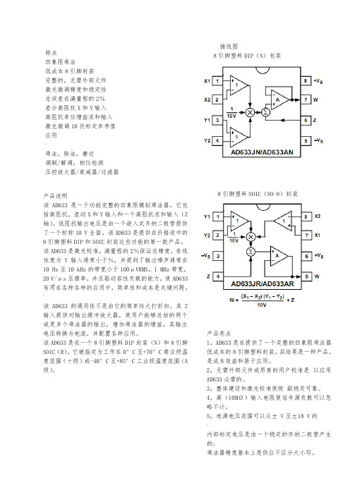
接线图8引脚塑料DIP (N )包装"~.特点 四象限乘法 低成本8引脚封装 完整的,无需外部元件 激光微调精度和稳定性 总误差在满量程的2% 差分高阻抗X 和Y 输入 高阻抗单位增益求和输入 激光微调10伏标定参考值 应用 ! 乘法,除法,磨边调制/解调,相位检测 压控放大器/衰减器/过滤器 产品说明 该AD633是一个功能完整的四象限模拟乘法器。
它包括高阻抗,差动X 和Y 输入和一个高阻抗求和输入(Z 轴)。
低阻抗输出电压是由一个嵌入式齐纳二极管提供了一个标称10 V 全面。
该AD633是提供在价格适中的8引脚塑料DIP 和SOIC 封装这些功能的第一款产品。
该AD633是激光校准,满量程的2%保证总精度。
非线性度为Y 输入通常小于%,并提到了输出噪声通常在10 Hz至10 kHz 的带宽小于100μVRMS 。
1 MHz 带宽,20 V/μs 压摆率,并且驱动容性负载的能力,使AD633有用在各种各样的应用中,简单性和成本是关键问题。
"该AD633的通用性不是由它的简单性大打折扣。
其Z 输入提供对输出缓冲放大器,使用户能够总结的两个或更多个乘法器的输出,增加乘法器的增益,其输出电压转换为电流,并配置各种应用。
该AD633是在一个8引脚塑料DIP 封装(N )和8引脚SOIC (R )。
它被指定为工作在0°C 至+70°C 商业级温度范围(十级)或-40°C 至+85°C 工业级温度范围(A 级)。
8引脚塑料SOIC (SO-8)封装 产品亮点1,AD633是在提供了一个完整的四象限乘法器 低成本的8引脚塑料封装。
其结果是一种产品,是成本效益和易于应用。
2,无需外部元件或昂贵的用户校准是 以应用AD633必需的。
3,整体建设和激光校准使脱 副稳定可靠。
4,高(10M Ω)输入电阻使信号源负载可以忽略不计。
5,电源电压范围可以从± V 至±18 V 的 /内部标定电压是由一个稳定的齐纳二极管产生的;乘法器精度基本上是供应不区分大小写。
- 1、下载文档前请自行甄别文档内容的完整性,平台不提供额外的编辑、内容补充、找答案等附加服务。
- 2、"仅部分预览"的文档,不可在线预览部分如存在完整性等问题,可反馈申请退款(可完整预览的文档不适用该条件!)。
- 3、如文档侵犯您的权益,请联系客服反馈,我们会尽快为您处理(人工客服工作时间:9:00-18:30)。
Design of an BJT analog multiplier1. IntroductionThe analog multiplier is a wildly used circuit that can take two analog inputs and produce an output proportional to their product. In modern IC industry, the analog multiplier is a very useful building block for the design of analog signal processing and the communication systems. Its application fields include signal modulation/demodulation, gain control, phase lock loops, frequency translation and waveform generation (Graeme, 1971). The purpose of this report is to explain the design method of a 4 quadrant analog multiplier using bipolar transistor. In this report, the theory of the analog multiplier is introduced. And then a suggested circuit based on the Gilbert multiplier provided. After that, the circuit simulation is processed with LTSPICE. In the last, the limitation and improvement of this design is being discussed.2. Principle of analog multiplier2.1 Characteristic of bipolar transistorThe basic cell of an analog multiplier is bipolar transistor. Here is a LTSPICE schematic diagram of a biased BJT.Fig.1. Schematic diagram of bipolar transistor Fig.2. I-V characteristic of bipolartransistorBecause of the semiconductor physical characteristic, the base-emitter voltage has an exponential relationship with the collector current (Ashburn, 2003). In most situations, the I-V characteristic can be written in the following equation:2exp()exp()nb i BE BE E C S th B AB qAD n V qV I I I V W N kT(Eq.1)Here, 2nb i S B AB qAD n I W N is saturation current of the base. th kT V q is thermal voltage, which can be considered equal to 26mV in room temperature. I C is the collector current. I E is the emitter current. V BE is the base-emitter voltage. I S is a constant which is determined by the geometric size of base and its doping density. V th is a constant which is only determined by the temperature. It can be seen from the equation that the collector current will exponential increase with the base-emitter voltage. Using LTSPICE DC simulation, the figure 2 can show this relationship directly. From the graph it can be seen that the I C equals nearly to 0 when V BE is less than 520mV. Also I C has a maximum value when V BE arrival 700mV. So the threshold voltage V T is in this range. And the exponential relationship only works in this range.2.2 Simple multiplierBased on the characteristic of bipolar transistor discussed above, a simple multiplier circuit can be developed. The structure of this circuit is shown in figure 3 and 4.Fig.3. the differential amplifier circuit Fig.4. 2 quadrant analog multiplier circuit In figure 3, Vx is the differential input. Io is the current source. Q1, Q2 are two NPN transistors. It can be seen that:And:According to these 2 equations, . From the Eq.1., we canobtain . In mathematics, when(about 2*26mV), . Thus we get:(Eq.2) The different current and can be used as the output, so we can get an output voltage which is proportional to the input voltage (Gray, 2001). This is:(Eq.3) The circuit of figure 4 is established on the circuit of figure 3. In this circuit, there isSubstitute this formula into the Eq.3, we have:(Eq.4) If, Eq.4 is approximately equal to:(Eq.5) In this equation, can be either positive or negative. But in order to ensure the Q3 is turned on, must be larger than , which means must be positive. Thus this analog multiplier can only work in 2 quadrants, the first quadrant and the second quadrant.2.3 The Gilbert CellThe basic Gilbert analog multiplier cell is presented in the figure 5.Fig.5 the circuit of Gilbert cellIn this circuit, the input voltage Vx and Vy can generate pairs of differential currents, which results in the collector currents of the transistors. According to Eq.2, there areThus, the combination of these 3 equations above gives the difference of two output currentsBecause the derivation of this derivation is based on the Eq.2, it must satisfy the same requirement, which is and . At this time, the output voltage isFrom this equation it can be seen that the output voltage is proportional to the product of Vx and Vy. However, different from the 2 quadrant multiplier, here the input signal Vy can be either positive or negative. So, an analog multiplier can be realised.3. Circuit design3.1 basic analog multiplier circuitThe circuit of the practical basic 4 quadrant multiplier build on the previous analysis is presented in the following figure.Fig.6 the 4 quadrant multiplier based on the Gilbert cellThe compositions of this circuit are resisters and transistors. For the rough design, current source is used directly. And the structure of two current sources is more sensitive than that of one current source, so the circuit will get a better balance characteristic. According to the analysis in 2.1, the exponential relationship between base-emitter voltage and collector current only remain in the range of 520mV-700mV. So the static base-emitter current can be chosen at 610mV, the middle point of thisrange. From figure 4, the corresponding collector current is about 0.2mA. In addition, the emitter current is approximately equal to the collector current. So 0.2mA can be set as the value of the current resources.In this circuit, the npn transistors are all 2N2222. It can be seen from the circuit that the function of the transistor pair Q7 and Q8 is transforming the voltage input signal into current input signal, so is the transistor pair Q5 and Q6. Thus, the multiplier operation is based on the variation of the currents. In addition, the four transistors Q7, Q8, Q9, Q10 and the resistor R2 consist of a block which can generate a signal of function. This current can compensate the function generated by the next transistors Q1, Q2, Q3 and Q4. Thus, the output current signal has no relationship with function, that means there is no limitation of (Gray, 2001). This feature significantly expands the input signal magnitude. The transistors Q5, Q6 and resistor R1 have the same feature and the limitation is also cancelled. The output of the nonlinear compensation block in the front of Gilbert cell isFor Ic7 and Ic8, there areSubstitute Ic7 and Ic8 into Eq.9, the output of the nonlinear compensation block is given byIn the Gilbert cell block, the emitter resistors of Q5 and Q6 are much smaller than R1, so we have . So Ic5 and Ic6 is given byUse Eq.11, Eq.12 and Eq.10 to calculate the output voltage based on the Eq.6, Eq.7 and Eq.8. Finally we can obtainFrom this equation and the above derivation, it can be seen that:When R1 and R2 is big enough, the output voltage Vo is proportional to theproduct of Vx and Vy. And the circuit will get the nearly ideal multiplierfunction.Both Vx and Vy can be positive and negative, so it is a 4 quadrant multiplier.The gain coefficient , which is determined by the paramount Rc,R1, R2 andK has no relationship with Vth, so this circuit has a nice thermal stability.In this circuit, because the current sources are all 0.2mA, a several independentcurrent sources based on the current mirror can be used.From Gray and Hurst, there are mainly 3 types of current mirrors: the simple current mirror, simple current mirror with beta () helper, and the Wilson current mirror (Gray, 2001). For the first one, the output current . For the third one, the outputcurrent is . It can easily be seen that the Wilson current mirror can geta much more precise output current. Thus, in this report, the Wilson current mirror isused as the current source. The whole structure is shown in figure 7.Fig.7 the circuit structure with mirror current sourceIn order to get a precise value of the current , a resistor is added between the Vdd and the current mirror transistor. The aimed current is 0.2mV, so the value of this resistor .Use LTSPICE to simulate the circuit. Here is the DC sweep for the circuit.Fig.8. The DC sweep simulation resultThe settings of this simulation are as the follows: sweep Vx from -13V to 13V, and the increment is 1V; sweep Vy from 13V to -13V, and the increment is 1V. During the design, it can be noticed that the magnitude of input signals have a proportional relationship with the product of and R1 (or R2). Besides, to get high amplitude of Vo, Eq.13 must be considered. In this report, the circuit has a nice linear range of output signal when the input signal varies from -13V to +13V. And the output signal has the same range with the input signals.In order to obtain this amplitude of output signal, the V dd and V EE are set up at +32V and -15V respectively.Transient simulation:Fig.8 simulation result for AC inputs Fig.10 simulation results for squareoperationThe settings of the simulation of figure 8 are as the follows:Vx: amplitude=13V; frequency=10 kHz; phase=0. Vy: amplitude=13V; frequency=10 kHz; phase=90o. The Vx input is a sin(t) signal, the Vy input is a cos(t) signal. In this simulation, the Vx and Vy contain all 4 quadrant inputs combinations in one period, which are (Vx>0, Vy>0), (Vx>0, Vy<0), (Vx<0, Vy<0), (Vx>0, Vy>0). So the results proved the circuit can work in 4 quadrants. Furthermore, the frequency of the output signal is twice as the input signals and the amplitude is about half of the input ones. These features satisfy the functionof. So the result proved the circuit can work as an analog multiplier.One useful application of analog multiplier is square operation. As the figure 10 shows, make the two pulse input signal same, then we can obtain a parabola output signal. So the results of can be calculated.Frequency response simulation:Fig.11 Simulation result of frequency responseThis figure shows the frequency response of the circuit. When theAmplitude-frequency characteristic decrease from -22dB to -25dB (increased by -3dB), the relative operation frequency is 500.4 kHz. Below this frequency, the circuit can work nicely.Another useful application of analog multiplier is modulator. In the modulator, the low frequency signal is used to modulate, and the high frequency signal acts as a carrier.Fig.12. modulator simulation: Vx has no DC offset Fig.13 modulator simulation: Vx has a 1.5V DC offsetIt can be seen from the above 2 figures, the frequency of the output signal can be changed by change the magnitude of the input signal.3.2 improvement of output signal amplifyThe output signal of the 3.1 circuit has double ends, which is not so convenient to the following circuits. Besides, for some applications, people need large output signals and a wide band width. This can be realised by adding a Double-ended input single-ended output circuit (shown in figure 14). This additional circuitconsist of a differential amplifier and a basic common collector circuit (shown infigure 15 and 16).Fig.14 2 ended inputs 1 ended output circuit Fig.15 LTP with activeloadFig.16 basic commoncollector circuitThe practical circuit with this addition output circuit is shown below.Fig.17 the circuit followed with 2 input ended 1 output ended circuit The DC sweep simulation is as follow (same setting as 3.1):Fig.18 the relative DC simulationCompared with figure 8, the output voltage increased, but the amplitude of output signal decreased. Furthermore, the common mode signal was amplified by the differential amplifier circuit, so the average value of output voltagebecomes to 22V. When Vx=0 or Vy=0, the output voltage equals to 22V. Thiscircuit can not operate as a multiplier. In a word, this additional circuit did not get the expected result.4. DiscussionAs the analysis showed in 3.1, the circuit of figure 6 can cancel the influence caused by temperature. This is because the differential and balance structure of the nonlinear composition block can remove the common mode signal. The temperature is physical paramount, which change by the same value in a small electric circuit. So noise caused by the temperature can be considered as the common mode signal. The circuit design in this report has a nice thermal stability.Use LTSPICE simulation, the power consumption of each and total elements can be detected easily. In order to reduce the power of the circuit, the current source should relatively be at a small value. But at the same time, the current should ensure the operation of the transistors.The limitation of this design is the same of the bipolar transistor. As the figure 2 shows, bipolar transistor has a limited exponential operation range. This feature asks for a highly accurate collector current control. To solve this problem, one way is to change the physical paramount of the transistor. For example, reduce the cross-section area. Another way is to use MOS transistors. Because the CMOS operation is based on the movement of majority carriers, there is no exponential relationship between drain current and drain-source voltage.5. ConclusionIn this report, an analog multiplier is proposed. Firstly, the principle of the design is introduced. Then a practical circuit is proposed. At the same time, the methods of how to change the paramount to achieve a suitable output signal are described. During the design, theory analyses and explains are also presented. The simulation is processed with LTSPICE. For this report, the results of simulation can satisfy the principle derivation. The designed circuit achieves its porpours.ReferenceGraeme.J.G., Tobey.G.E. and Huelsman. L.P. 1971. Operational Amplifiers: Design and Application. New York: McGRAW-HILL Book Company. (p.397-398)Peter Ashburn. 2003. SiGe Heterojunction Bipolar Transistors. West Sussex: John Wiley & Sons Ltd.GRAY Paul R. Analysis and design of analog integrated circuits. New York: John Wiley & Sons Ltd.。