合勤NXC5200
MPC5200中文简述
: 主要特点如下所示。 mpc603e 系列 G2_LE 核心 ——超标量体系结构的体系结构 - 760 MIPS 在 400 MHz(400 + 85 摄氏度) - 16 k 指令缓存,16 k 数据缓存 ——双精度 FPU MMU -指令和数据 ——标准和关键的中断功能 内部/ DDR 内存接口 - 132 - mhz 操作 ——更快和 DDR SDRAM 的支持 每 CS - 256 兆字节寻址范围,可用两个 CS ——32 位数据总线 ——内置的初始化和更新 测试/调试功能 JTAG(IEEE 1149.1 测试访问端口) ——常见的芯片上的处理器(COP)调试端口 车载锁相环和时钟的一代
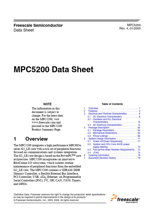
飞思卡尔半导体 中文数据表
MPC5200
MPC5200 数据表
请注意 本文档中的信息是可能发生变化。请关注 MPC5200 的最新数据。
概述
MPC5200 集成了一系列高性能 MPC603e G2_LE 核心与一组丰富的外围功能集中在通信 和系统集成。G2_LE 核心设计是基于 PowerPCTM 核心架构。MPC5200 包含一个创新 BestComm I / O 子系统,该隔离日常维护嵌入式 G2_LE 外围功能的核心。MPC5200 包含一个内部/ DDR 内存控制器,一个灵活的外部总线接口,PCI 控制器、USB、ATA,Etherne
霍尼韦尔门禁报价
产品型号描述Pro-Watch CE公司版管理软件 (CE) 3.8PWCESW8Pro-Watch 3.80 公司版服务器软件- (1个) 服务器软件许可证, (1个)PWCESW8CPro-Watch 3.80 公司版服务器软件- (1个) 服务器软件许可证, (1个)PW8SWCLPW3.80 PE/CE 单用户软件许可证PW8RDR32PWPE 和PWCE 32 读卡器软件许可证PW8RDR64PWPE 和PWCE 64 读卡器软件许可证PW8RDR128PWPE 和PWCE 128 读卡器软件许可证PW8RDR256PWPE 和PWCE 256 读卡器软件许可证PW8RDR512PWPE 和PWCE 512 读卡器软件许可证PW8MEDIA英文版PW3.80CD PW8BADGELPW3.80 PE/CE 传统并发卡证打印软件许可证PW8ABADGELPW3.80 PE/CE 高级并发卡证打印软件许可证冗余软件和冗余软件狗PWCESW8-RPro-Watch 3.80 公司版服务器软件- (1个) 服务器软件许可证, (1个)PWCESW8C-RPro-Watch 3.80 公司版服务器软件- (1个) 服务器软件许可证, (1个)PW8SWCL-R单用户企业工作站许可证-冗余PWCE8RDR32-RPWPE 和PWCE 32 读卡器软件许可证-冗余PWCE8RDR64-RPWPE 和PWCE 64 读卡器软件许可证-冗余PWCE8RDR128-RPWPE 和PWCE 128 读卡器软件许可证-冗余PWCE8RDR256-RPWPE 和PWCE 256 读卡器软件许可证-冗余PWCE8RDR512-RPWPE 和PWCE 512 读卡器软件许可证-冗余PW8BADGEL-R传统发卡证打印软件许可证PW8ABADGEL-R高级发卡证打印软件许可证Pro-Watch EE 公司版管理软件 (EE) 3.8PWEESW8Pro-Watch 3.80 企业版服务器软件- (1个) 企业版服务器许可, (1个)PWEE8SWCL单用户企业工作站许可PWEE8SWRS单区域服务器许可软件升级PWCR8UPGPro-Watch 公司版服务器软件3.7x 版升级3.80版, 60天质保期PWER8UPGPro-Watch 企业版服务器软件3.7x 版升级3.80版, 60天质保期UPG8ABADGEL PW3.80 PE/CE 传统并发卡证打印升级到高级并发卡证打印软件许Pro-Watch CE 公司版管理软件 (CE) 3.7PWCESW7Pro-Watch 公司版服务器软件- (1个) 服务器软件狗, (1个) 并发用户PWCE7SWCL单用户软件狗PWCE7SWCL55用户软件狗PWCE7SWCL1010用户软件狗PWCE7SWCL1515用户软件狗PWCE7SWCL2020用户软件狗PWCE7RDR3232 读卡器软件许可证PWCE7RDR6464 读卡器软件许可证PWCE7RDR128128 读卡器软件许可证PWCE7RDR256256 读卡器软件许可证PWCE7RDR512512读卡器软件许可证PWCE7BADGEL发卡证打印软件狗冗余软件和冗余软件狗PWCESW7-RPro-Watch 公司版服务器软件- (1个) 服务器软件狗, (1个) 并发用户PWCE7SWCL-R单用户软件狗 -冗余PWCE7SWCL5-R5用户软件狗-冗余PWCE7SWCL10-R 10用户软件狗-冗余< 2010霍尼韦尔企业级安防产品经销商价格表 - 门禁管理系Honeywell Security -China 生效日期:2011年4月1日¥58,928.99¥56,033.34¥12,192.20¥12,446.21¥24,384.41¥45,720.77¥90,425.51¥171,706.87¥406.41¥20,117.14¥30,277.31¥29,464.49¥26,360.56¥6,096.10¥6,223.10¥12,192.20¥22,860.38¥45,212.76¥85,853.44¥10,058.57¥15,138.65¥396,185.67¥18,288.31¥104,852.95¥36,820.46¥118,264.38¥10,160.17¥63,265.35¥19,507.53¥79,249.33¥158,498.65¥205,865.36¥262,193.35¥12,446.21¥24,384.41¥45,720.77¥90,425.51¥171,706.87¥24,140.56¥31,632.67¥9,753.76¥39,624.66¥79,249.33¥131,096.67¥6,223.10¥12,192.20¥22,860.38¥45,212.76¥85,853.44¥12,070.28¥396,187.43¥19,202.72¥91,187.53¥172,824.49¥244,809.30¥307,243.54¥104,852.95¥239,475.21¥480,017.23¥722,946.90¥971,413.86¥55,880.94¥19,583.65¥164,228.33¥30,480.51¥20,269.54¥0.00¥8,493.90¥8,397.38¥8,204.34¥0.00¥4,572.08¥4,368.87¥5,080.09¥1,097.30¥5,740.50¥279.24¥5,689.70¥1,428.59¥1,538.48¥3,186.86¥61.28¥61.12¥61.28¥112.42¥809.73¥809.73¥1,110.49¥17.35¥23.14¥1,388.11¥2,602.70¥2,487.02¥4,800.54¥3,123.24¥6,535.67¥74.50¥74.50¥125.20¥124.93¥92.54¥108.27¥179.98¥179.59¥201.89¥199.85¥174.47¥80.97¥169.04¥126.66¥1,214.59¥1,214.59¥1,850.81¥2,834.05¥2,834.05¥3,817.29¥7,923.78¥32.39¥2,240.00¥8,800.00¥12,724.31¥13,881.07¥14,459.45¥4,627.02¥5,783.78¥13,881.07¥462.70¥853.15¥853.15¥924.32¥1,086.73¥1,782.48¥1,144.88¥1,306.29¥200.50¥335.84¥174.44¥155.39¥453.14¥420.06¥374.94¥150.38¥114.29¥114.29¥194.49¥219.55¥501.26¥250.63¥310.78¥310.78¥323.81¥323.81¥1,306.29¥1,306.29¥36,240.47¥59,940.78¥3,840.05¥3,600.05¥3,600.05¥124,561.63¥56,640.74。
MPC5200资料
Freescale Semiconductor Data SheetMPC5200Rev. 4, 01/2005 Table of ContentsNOTEThe information in thisdocument is subject tochange. For the latest dataon the MPC5200, visit andproceed to the MPC5200Product Summary Page.1OverviewThe MPC5200 integrates a high performance MPC603e series G2_LE core with a rich set of peripheral functions focused on communications and systems integration. The G2_LE core design is based on the PowerPC TM core architecture. MPC5200 incorporates an innovative BestComm I/O subsystem, which isolates routine maintenance of peripheral functions from the embedded G2_LE core. The MPC5200 contains a SDRAM/DDR Memory Controller, a flexible External Bus Interface, PCI Controller, USB, ATA, Ethernet, six Programmable Serial Controllers (PSC), I2C, SPI, CAN, J1850, Timers, and GPIOs.1Overview. . . . . . . . . . . . . . . . . . . . . . . . . . . . . . . . 1 2Features . . . . . . . . . . . . . . . . . . . . . . . . . . . . . . . . 2 3Electrical and Thermal Characteristics. . . . . . . . . 63.1DC Electrical Characteristics. . . . . . . . . . . . . 63.2Oscillator and PLL ElectricalCharacteristics. . . . . . . . . . . . . . . . . . . . . . . 123.3AC Electrical Characteristics. . . . . . . . . . . . 14 4Package Description. . . . . . . . . . . . . . . . . . . . . . 644.1Package Parameters. . . . . . . . . . . . . . . . . . 644.2Mechanical Dimensions. . . . . . . . . . . . . . . . 644.3Pinout Listings. . . . . . . . . . . . . . . . . . . . . . . 66 5System Design Information. . . . . . . . . . . . . . . . . 715.1Power UP/Down Sequencing . . . . . . . . . . . 715.2System and CPU Core AVDD powersupply filtering . . . . . . . . . . . . . . . . . . . . . . . 735.3Pull-up/Pull-down Resistor Requirements. . 735.4JTAG . . . . . . . . . . . . . . . . . . . . . . . . . . . . . . 74 6Ordering Information. . . . . . . . . . . . . . . . . . . . . . 79 7Document Revision History. . . . . . . . . . . . . . . . . 79MPC5200 Data SheetFeatures2FeaturesKey features are shown below.•MPC603e series G2_LE core—Superscalar architecture—760 MIPS at 400 MHz (-40 to +85 o C)—16 k Instruction cache, 16 k Data cache—Double precision FPU—Instruction and Data MMU—Standard and Critical interrupt capability•SDRAM / DDR Memory Interface—up to 132-MHz operation—SDRAM and DDR SDRAM support—256-MByte addressing range per CS, two CS available—32-bit data bus—Built-in initialization and refresh•Flexible multi-function External Bus Interface—Supports interfacing to ROM/Flash/SRAM memories or other memory mapped devices —8 programmable Chip Selects—Non multiplexed data access using 8/16/32 bit databus with up to 26-bit address—Short or Long Burst capable—Multiplexed data access using 8/16/32 bit databus with up to 25-bit address •Peripheral Component Interconnect (PCI) Controller—Version 2.2 PCI compatibility—PCI initiator and target operation—32-bit PCI Address/Data bus—33- and 66-MHz operation—PCI arbitration function•ATA Controller—Version 4 ATA compatible external interface—IDE Disk Drive connectivity •BestComm DMA subsystem—Intelligent virtual DMA Controller—Dedicated DMA channels to control peripheral reception and transmission—Local memory (SRAM 16 kBytes)• 6 Programmable Serial Controllers (PSC), configurable for the following:—UART or RS232 interfaceFeatures—CODEC interface for Soft Modem, Master/Slave CODEC Mode, I2S and AC97—Full duplex SPI mode—IrDA mode from 2400 bps to 4 Mbps•Fast Ethernet Controller (FEC)—Supports 100Mbps IEEE 802.3 MII, 10 Mbps IEEE 802.3 MII, 10 Mbps 7-wire interface •Universal Serial Bus Controller (USB)—USB Revision 1.1 Host—Open Host Controller Interface (OHCI)—Integrated USB Hub, with two ports.•Two Inter-Integrated Circuit Interfaces (I2C)•Serial Peripheral Interface (SPI)•Dual CAN 2.0 A/B Controller (MSCAN)—Freescale Scalable Controller Area Network (F SCAN) architecture—Implementation of version 2.0A/B CAN protocol—Standard and extended data frames•J1850 Byte Data Link Controller (BDLC)—J1850 Class B data communication network interface compatible and ISO compatible for low speed (<125 kbps) serial data communications in automotive applications.—Supports 4X mode, 41.6 kbps—In-frame response (IFR) types 0, 1, 2, and 3 supported•Systems level features—Interrupt Controller supports four external interrupt request lines and 47 internal interrupt sources—GPIO/Timer functions–Up to 56 total GPIO pins (depending on functional multiplexing selections) that support a variety of interrupt/WakeUp capabilities.–Eight GPIO pins with timer capability supporting input capture, output compare, and pulse width modulation (PWM) functions—Real-time Clock with one-second resolution—Systems Protection (watch dog timer, bus monitor)—Individual control of functional block clock sources—Power management: Nap, Doze, Sleep, Deep Sleep modes—Support of WakeUp from low power modes by different sources (GPIO, RTC, CAN)Features•Test/Debug features—JTAG (IEEE 1149.1 test access port)—Common On-chip Processor (COP) debug port •On-board PLL and clock generationFigure1 shows a simplified MPC5200 block diagram.FeaturesFigure 1. Simplified Block Diagram—MPC5200603G 2_L E C o r eS D R A M / D D R J T A G / C O P I n t e r f a c eR e s e t / C l o c k MSCAN R e a l -T i m e C l o c kS y s t e m F u n c t i o n sI n t e r r u p t C o n t r o l l e rG P I O /T i m e r sP C I B u s C o n t r o l l e rL o c a l P l u s C o n t r o l l e r A T A H o s t C o n t r o l l e rS y s t e m s I n t e r f a c e U n i t (S I U )S D R A M / D D RC o m m B u sL o c a l BestComm DMASRAM 16KB u sJ1850USB SPII 2C EthernetPSC M e m o r y C o n t r o l l e rG e n e r a t i o n2x2x2x6xElectrical and Thermal Characteristics3Electrical and Thermal Characteristics3.1DC Electrical Characteristics3.1.1Absolute Maximum RatingsThe tables in this section describe the MPC5200 DC Electrical characteristics. Table 1 gives the absolute maximum ratings.3.1.2Recommended Operating ConditionsTable 2 gives the recommended operating conditions.Table 1. Absolute Maximum Ratings 1NOTES:1Absolute maximum ratings are stress ratings only, and functional operation at the maximums is not guaranteed. Stresses beyond those listed may affect device reliability or cause permanent damage.CharacteristicSymbol Min Max Unit SpecID Supply voltage - G2_LE core and peripheral logic VDD_CORE –0.3 1.8V D1.1Supply voltage - I/O buffers VDD_IO,VDD_MEM_IO –0.3 3.6V D1.2Supply voltage - System APLL SYS_PLL_AVDD –0.3 2.1V D1.3Supply voltage - G2_LE APLL CORE_PLL_AVDD–0.3 2.1V D1.4Input voltage (VDD_IO)Vin –0.3VDD_IO + 0.3V D1.5Input voltage (VDD_MEM_IO)Vin –0.3VDD_MEM_IO+ 0.3V D1.6Input voltage overshoot Vinos – 1.0V D1.7Input voltage undershoot Vinus – 1.0VD1.8Storage temperature rangeTstg–55150oCD1.9Table 2. Recommended Operating ConditionsCharacteristicSymbol Min 1Max (1)Unit SpecID Supply voltage - G2_LE core and peripheral logicVDD_CORE 1.42 1.58V D2.1Supply voltage - standard I/O buffers VDD_IO 3.0 3.6V D2.2Supply voltage - memory I/O buffers (SDR)VDD_MEM_IO SDR 3.0 3.6V D2.3Supply voltage - memory I/O buffers (DDR)VDD_MEM_IO DDR 2.42 2.63V D2.4Supply voltage - System APLL SYS_PLL_AVDD 1.42 1.58V D2.5Supply voltage - G2_LE APLL CORE_PLL_AVDD1.42 1.58V D2.6Input voltage - standard I/O buffers Vin 0VDD_IO V D2.7Input voltage - memory I/O buffers (SDR)Vin SDRVDD_MEM_IO SDRVD2.8Electrical and Thermal Characteristics3.1.3DC Electrical SpecificationsTable 3 gives the DC Electrical characteristics for the MPC5200 at recommended operating conditions (see Table 2).Input voltage - memory I/O buffers (DDR)Vin DDR 0VDD_MEM_IO DDRVD2.9Ambient operating temperature range 2T A -40+85o C D2.10Extended ambient operating temperature range 3T Aext -40+105oCD2.11Die junction operating temperature range Tj -40+115o C D2.12Extended die junction operating temperature rangeTjext-40+125o CD2.13NOTES:1These are recommended and tested operating conditions. Proper device operation outside these conditions is not guaranteed.2Maximum G2_LE core operating frequency is 400 MHz 3Maximum G2_LE core operating frequency is 264 MHzTable 3. DC Electrical SpecificationsCharacteristicConditionSymbol Min Max Unit SpecID Input high voltage Input type = TTLVDD_IO/VDD_MEM_IO SDRV IH 2.0—V D3.1Input high voltage Input type = TTL VDD_MEM_IO DDR V IH 1.7—V D3.2Input high voltage Input type = PCIVDD_IO V IH 2.0—V D3.3Input high voltage Input type = SCHMITTVDD_IOV IH 2.0—V D3.4Input high voltage SYS_XTAL_IN CV IH 2.0—V D3.5Input high voltage RTC_XTAL_IN CV IH 2.0—V D3.6Input low voltage Input type = TTLVDD_IO/VDD_MEM_IO SDRV IL —0.8V D3.7Input low voltage Input type = TTL VDD_MEM_IO DDR V IL —0.7V D3.8Input low voltage Input type = PCIVDD_IO V IL —0.8V D3.9Input low voltage Input type = SCHMITTVDD_IOV IL —0.8V D3.10Input low voltage SYS_XTAL_IN CV IL —0.8V D3.11Input low voltageRTC_XTAL_INCV IL—0.8VD3.12Table 2. Recommended Operating Conditions (continued)CharacteristicSymbol Min 1Max (1)Unit SpecIDElectrical and Thermal CharacteristicsInput leakage currentVin = 0 orVDD_IO/VDD_IO_MEM SDR(depending on input type 1)I IN—+10µAD3.13Input leakage current SYS_XTAL_IN Vin = 0 or VDD_IO I IN —+10µA D3.14Input leakage current RTC_XTAL_IN Vin = 0 or VDD_IOI IN —+10µA D3.15Input current, pullup resistorPULLUP VDD_IO Vin = 0I INpu40109µAD3.16Input current, pullup resistor - memory I/O buffersPULLUP_MEM VDD_IO_MEM SDRVin = 0I INpu41111µA D3.17Input current, pulldown resistorPULLDOWN VDD_IO Vin = VDD_IOI INpd36106µA D3.18Output high voltage IOH is driver dependent 2VDD_IO, VDD_IO_MEM SDR V OH 2.4—V D3.19Output high voltage IOH is driver dependent 2VDD_IO_MEM DDR V OHDDR 1.7—V D3.20Output low voltage IOL is driver dependent 2VDD_IO, VDD_IO_MEM SDR V OL —0.4V D3.21Output low voltageIOL is driver dependent 2VDD_IO_MEM DDRV OLDDR —0.4V D3.22DC Injection Current Per Pin 3I CS-1.0 1.0mA D3.23CapacitanceVin = 0V , f = 1 MHzC in—15pFD3.24NOTES:1Leakage current is measured with output drivers disabled and pull-up/pull-downs inactive.2See Table 4 for the typical drive capability of a specific signal pin based on the type of output driver associated with that pin as listed in Table 52.3All injection current is transferred to VDD_IO/VDD_IO_MEM. An external load is required to dissipate this current to maintain the power supply within the specified voltage range.Total injection current for all digital input-only and all digital input/output pins must not exceed 10 mA. Exceeding this limit can cause disruption of normal operation.Table 4. Drive Capability of MPC5200 Output PinsDriver Type Supply Voltage I OH I OL Unit SpecID DRV4VDD_IO = 3.3V 44mA D3.25DRV8VDD_IO = 3.3V88mAD3.26Table 3. DC Electrical Specifications (continued)CharacteristicConditionSymbol Min Max Unit SpecIDElectrical and Thermal Characteristics3.1.4Electrostatic DischargeCAUTIONThis device contains circuitry that protects against damage due tohigh-static voltage or electrical fields. However, it is advised that normal precautions be taken to avoid application of any voltages higher than maximum-rated voltages. Operational reliability is enhanced if unused inputs are tied to an appropriate logic voltage level (i.e., either GND or V CC ). Table 7 gives package thermal characteristics for this device.3.1.5Power DissipationPower dissipation of the MPC5200 is caused by 3 different components: the dissipation of the internal or core digital logic (supplied by VDD_CORE), the dissipation of the analog circuitry (supplied by SYS_PLL_A VDD and CORE_PLL_A VDD) and the dissipation of the IO logic (supplied byVDD_IO_MEM and VDD_IO). Table 6 details typical measured core and analog power dissipation figures for a range of operating modes. However, the dissipation due to the switching of the IO pins can not be given in general, but must be calculated by the user for each application case using the following formulaDRV8_OD VDD_IO = 3.3V -8mA D3.27DRV16_MEM VDD_IO_MEM = 3.3V 1616mA D3.28DRV16_MEM VDD_IO_MEM = 2.5V 1616mA D3.29PCIVDD_IO = 3.3V1616mAD3.30Table 5. ESD and Latch-Up Protection CharacteristicsSym RatingMin Max Unit SpecID V HBM Human Body Model (HBM)—JEDEC JESD22-A114-B 2000—V D4.1V MMMachine Model (MM)—JEDEC JESD22-A115200—V D4.2V CDM Charge Device Model (CDM)—JEDEC JESD22-C101500—V D4.3I LATLatch-up Current at T A =85o C positive negative+100-100—mAD4.4I LATLatch-up Current at T A =27o C positive negative+200-200—mAD4.5Table 4. Drive Capability of MPC5200 Output Pins (continued)Driver Type Supply Voltage I OH I OL Unit SpecID P IO P IOint N M∑+C VDD _IO 2f×××=Electrical and Thermal Characteristicswhere N is the number of output pins switching in a group M, C is the capacitance per pin, VDD_IO is the IO voltage swing, f is the switching frequency and PIOint is the power consumed by the unloaded IO stage. The total power consumption of the MPC5200 processor must not exceed the value, which would cause the maximum junction temperature to be exceeded.Table 6. Power DissipationCore Power Supply (VDD_CORE)SpecIDModeSYS_XTAL/XLB/PCI/IPG/CORE (MHz)Unit Notes33/66/33/33/26433/132/66/132/396TypTyp Operational 727.51080mW 1,2NOTES:1Typical core power is measured at VDD_CORE = 1.5 V , Tj = 25 C 2Operational power is measured while running an entirely cache-resident program with floating-point multiplication instructions in parallel with a continuous PCI transaction via BestComm.D5.1Doze —600mW 1,33Doze power is measured with the G2_LE core in Doze mode, the system oscillator, System PLL and Core PLL are active, all other system modules are inactive D5.2Nap —225mW 1,44Nap power is measured with the G2_LE core in Nap mode, the stem oscillator, System PLL and Core PLL are active, all other system modules are inactive D5.3Sleep —225mW 1,55Sleep power is measured with the G2_LE core in Sleep mode, the stem oscillator, System PLL and Core PLL are active, all other system modules are inactiveD5.4Deep-Sleep52.552.5mW1,66Deep-Sleep power is measured with the G2_LE core in Sleep mode, the stem oscillator, System PLL, Core PLL and all other system modules are inactive D5.5PLL Power Supplies (SYS_PLL_AVDD, CORE_PLL_AVDD)Mode Typ Unit NotesT ypical2mW77Typical PLL power is measured at SYS_PLL_AVDD = CORE_PLL_AVDD = 1.5 V , Tj = 25 CD5.6Unloaded I/O Power Supplies (VDD_IO, VDD_MEM_IO 8)8IO power figures given in the table represent the worst case scenario. For the mem_io rail connected to 2.5V the IO power is expected to be lower and bounded by the worst case with VDD_MEM_IO connected to 3.3V .Mode Typ Unit NotesT ypical33mW99Unloaded typical I/O power is measured in Deep-Sleep mode at VDD_IO = VDD_MEM_IOSDR = 3.3 V , Tj = 25 CD5.7P total P core P analog P IO ++=Electrical and Thermal Characteristics3.1.6Thermal Characteristics3.1.7Heat DissipationAn estimation of the chip-junction temperature, T J , can be obtained from the following equation:T J =T A +(R θJA × P D )Eqn.1where:T A =ambient temperature for the package (°C)R θJA =junction to ambient thermal resistance (°C/W)P D =power dissipation in package (W)The junction to ambient thermal resistance is an industry standard value, which provides a quick and easy estimation of thermal performance. Unfortunately, there are two values in common usage: the value determined on a single layer board, and the value obtained on a board with two planes. For packages such as the PBGA, these values can be different by a factor of two. Which value is correct depends on the power dissipated by other components on the board. The value obtained on a single layer board is appropriate for the tightly packed printed circuit board. The value obtained on the board with the internal planes is usually appropriate if the board has low power dissipation and the components are well separated.Table 7. Thermal Resistance DataRatingValueUnit NotesSpecID Junction to Ambient Natural Convection Single layer board (1s)R θJA 30°C/W 1,2NOTES:1Junction temperature is a function of die size, on-chip power dissipation, package thermal resistance, mounting site (board) temperature, ambient temperature, air flow, power dissipation of other components on the board, and board thermal resistance.2Per SEMI G38-87 and JEDEC JESD51-2 with the single layer board horizontal.D6.1Junction to Ambient Natural ConvectionFour layer board (2s2p)R θJMA 22°C/W 1,33Per JEDEC JESD51-6 with the board horizontal.D6.2Junction to Ambient (@200 ft/min)Single layer board (1s)R θJMA 24°C/W 1,3D6.3Junction to Ambient (@200 ft/min)Four layer board (2s2p)R θJMA 19°C/W 1,3D6.4Junction to Board R θJB 14°C/W 44Thermal resistance between the die and the printed circuit board per JEDEC JESD51-8. Board temperature is measured on the top surface of the board near the package.D6.5Junction to Case R θJC8°C/W 55Thermal resistance between the die and the case top surface as measured by the cold plate method (MIL SPEC-883 Method 1012.1).D6.6Junction to Package T opNatural ConvectionΨJT2°C/W66Thermal characterization parameter indicating the temperature difference between package top and the junction temperature per JEDEC JESD51-2. When Greek letters are not available, the thermal characterization parameter is written as Psi-JT.D6.7Electrical and Thermal CharacteristicsHistorically, the thermal resistance has frequently been expressed as the sum of a junction to case thermal resistance and a case to ambient thermal resistance:RθJA=RθJC+RθCA Eqn.2 where:RθJA=junction to ambient thermal resistance (°C/W)RθJC=junction to case thermal resistance (°C/W)RθCA=case to ambient thermal resistance (°C/W)RθJC is device related and cannot be influenced by the user. The user controls the thermal environment to change the case to ambient thermal resistance, RθCA. For instance, the user can change the air flow around the device, add a heat sink, change the mounting arrangement on printed circuit board, or change the thermal dissipation on the printed circuit board surrounding the device. This description is most useful for ceramic packages with heat sinks where some 90% of the heat flow is through the case to the heat sink to ambient. For most packages, a better model is required.A more accurate thermal model can be constructed from the junction to board thermal resistance and the junction to case thermal resistance1-3. The junction to case covers the situation where a heat sink will be used or where a substantial amount of heat is dissipated from the top of the package. The junction to board thermal resistance describes the thermal performance when most of the heat is conducted to the printed circuit board. This model can be used for either hand estimations or for a computational fluid dynamics (CFD) thermal model.To determine the junction temperature of the device in the application after prototypes are available, the Thermal Characterization Parameter (ΨJT) can be used to determine the junction temperature with a measurement of the temperature at the top center of the package case using the following equation:T J=T T+(ΨJT× P D)Eqn.3 where:T T=thermocouple temperature on top of package (°C)ΨJT=thermal characterization parameter (°C/W)P D=power dissipation in package (W)The thermal characterization parameter is measured per JESD51-2 specification using a 40-gauge type T thermocouple epoxied to the top center of the package case. The thermocouple should be positioned, so that the thermocouple junction rests on the package. A small amount of epoxy is placed over the thermocouple junction and over approximately one mm of wire extending from the junction. The thermocouple wire is placed flat against the package case to avoid measurement errors caused by cooling effects of the thermocouple wire.3.2Oscillator and PLL Electrical CharacteristicsThe MPC5200 System requires a system-level clock input SYS_XTAL. This clock input may be driven directly from an external oscillator or with a crystal using the internal oscillator.Electrical and Thermal CharacteristicsThere is a separate oscillator for the independent Real-Time Clock (RTC) system. The MPC5200 clock generation uses two phase locked loop (PLL) blocks. •The system PLL (SYS_PLL) takes an external reference frequency and generates the internal system clock. The system clock frequency is determined by the external reference frequency and the settings of the SYS_PLL configuration.•The G2_LE core PLL (CORE_PLL) generates a master clock for all of the CPU circuitry. The G2_LE core clock frequency is determined by the system clock frequency and the settings of the CORE_PLL configuration.3.2.1System Oscillator Electrical Characteristics3.2.2RTC Oscillator Electrical Characteristics3.2.3System PLL Electrical CharacteristicsTable 8. System Oscillator Electrical CharacteristicsCharacteristicSymbol NotesMin Typical Max Unit SpecID SYS_XT AL frequency f sys_xtal 15.633.335.0MHz O1.1Oscillator start-up timet up_osc——100µsO1.2Table 9. RTC Oscillator Electrical CharacteristicsCharacteristicSymbol NotesMin Typical Max Unit SpecID RTC_XTAL frequencyf rtc_xtal—32.768—kHzO2.1Table 10. System PLL SpecificationsCharacteristicSymbol NotesMin Typical Max Unit SpecID SYS_XT AL frequency f sys_xtal 1NOTES:1The SYS_XTAL frequency and PLL Configuration bits must be chosen such that the resulting system frequency, CPU (core) frequency, and PLL (VCO) frequency do not exceed their respective maximum or minimum operating frequencies.15.633.335.0MHz O3.1SYS_XT AL cycle time T sys_xtal (1)66.630.028.5ns O3.2SYS_XT AL clock input jitter t jitter 22This represents total input jitter - short term and long term combined - and is guaranteed by design. T wo different types of jitter can exist on the input to core_sysclk, systemic and true random jitter. True random jitter is rejected, but the PLL. Systemic jitter will be passed into and through the PLL to the internal clock circuitry, directly reducing the operating frequency.——150ps O3.3System VCO frequency f VCOsys (1)250533800MHz O3.4System PLL relock timet lock33Relock time is guaranteed by design and characterization. PLL-relock time is the maximum amount of time required for the PLL lock after a stable Vdd and core_sysclk are reached during the power-on reset sequence. This specification also applies when the PLL has been disabled and subsequently re-enabled during sleep modes.——100µsO3.5Electrical and Thermal Characteristics3.2.4G2_LE Core PLL Electrical CharacteristicsThe internal clocking of the G2_LE core is generated from and synchronized to the system clock by means of a voltage-controlled core PLL.3.3AC Electrical CharacteristicsHyperlinks to the indicated timing specification sections are provided below.AC Test Timing Conditions:Unless otherwise noted, all test conditions are as follows:Table 11. G2_LE PLL SpecificationsCharacteristicSymbol NotesMin Typical Max Unit SpecID G2_LE frequency f core 1NOTES:1The XLB_CLK frequency and G2_LE PLL Configuration bits must be chosen such that the resulting systemfrequencies, CPU (core) frequency, and G2_LE PLL (VCO) frequency do not exceed their respective maximum or minimum operating frequencies.50—550MHz O4.1G2_LE cycle time t core (1) 2.85—40.0ns O4.2G2_LE VCO frequency f VCOcore (1)400—1200MHz O4.3G2_LE input clock frequency f XLB_CLK 25—367MHz O4.4G2_LE input clock cycle time t XLB_CLK 2.73—50.0ns O4.5G2_LE input clock jitter t jitter 22This represents total input jitter - short term and long term combined - and is guaranteed by design. T wo different types of jitter can exist on the input to core_sysclk, systemic and true random jitter. True random jitter is rejected, but the PLL. Systemic jitter will be passed into and through the PLL to the internal clock circuitry, directly reducing the operating frequency.——150ps O4.6G2_LE PLL relock timet lock33Relock time is guaranteed by design and characterization. PLL-relock time is the maximum amount of time required for the PLL lock after a stable Vdd and core_sysclk are reached during the power-on reset sequence. This specification also applies when the PLL has been disabled and subsequently re-enabled during sleep modes.——100µsO4.7•AC Operating Frequency Data •USB •Clock AC Specifications •SPI •Resets•MSCAN •External Interrupts •I 2C •SDRAM •J1850•PCI•PSC•Local Plus Bus •GPIOs and Timers•ATA •IEEE 1149.1 (JTAG) AC Specifications•EthernetElectrical and Thermal Characteristics•TA = -40 to 85 o C •Tj = -40 to 115 o C•VDD_CORE = 1.42 to 1.58 V VDD_IO = 3.0 to 3.6 V •Input conditions:All Inputs: tr, tf <= 1 ns •Output Loading:All Outputs: 50 pF3.3.1AC Operating Frequency DataTable 12 provides the operating frequency information for the MPC5200.3.3.2Clock AC SpecificationsFigure 2. Timing Diagram—SYS_XTAL_INTable 12. Clock FrequenciesMinMax Units SpecID 1G2_LE Processor Core —400MHz A1.12SDRAM Clock —133MHz A1.23XL Bus Clock —133MHz A1.34IP Bus Clock—133MHz A1.45PCI / Local Plus Bus Clock —66MHz A1.56PLL Input Range15.635MHzA1.6t FALLt RISEt CYCLE SYSCLKt DUTY t DUTY CV IHCV ILV MV MV MElectrical and Thermal Characteristics3.3.3ResetsThe MPC5200 has three reset pins: •PORRESET - Power on Reset •HRESET - Hard Reset •SRESET - Software ResetThese signals are asynchronous I/O signals and can be asserted at any time. The input side uses a Schmitt trigger and requires the same input characteristics as other MPC5200 inputs, as specified in the DC Electrical Specifications section. Table 14 specifies the pulse widths of the Reset inputs.Notes:1.its minimum pulse width equals the minimum given for HRESET related to the same reference clock.2.The t VDD_stable describes the time which is needed to get all power supplies stable.3.For t lock, refer to the Oscillator/PLL section of this specification for further details.4.For t up_osc, refer to the Oscillator/PLL section of this specification for further details.5.Following the deassertion of PORRESET , HRESET and SRESET remain low for 4096 reference clock cycles.6.clock cycles.NOTEAs long as VDD is not stable the HRESET output is not stable.Table 13. SYS_XTAL_IN TimingSym DescriptionMin Max Units SpecID t CYCLE SYS_XT AL_IN cycle time.1NOTES:1CAUTION —The SYS_XT AL_IN frequency and system PLL_CFG[0-6] settings must be chosen such that theresulting system frequencies do not exceed their respective maximum or minimum operating frequencies. See the MPC5200 User Manual [1].28.664.1ns A2.1t RISE SYS_XT AL_IN rise time.— 5.0ns A2.2t FALL SYS_XT AL_IN fall time.— 5.0ns A2.3t DUTY SYS_XT AL_IN duty cycle (measured at V M ).2 2SYS_XTAL_IN duty cycle is measured at V M .40.060.0%A2.4CV IH SYS_XT AL_IN input voltage high 2.0—V A2.5CV ILSYS_XT AL_IN input voltage low—0.8VA2.6Table 14. Reset Pulse WidthName Description Min Pulse Width Max Pulse WidthReference Clock SpecID PORRESET Power On Reset t VDD_stable +t up_osc +t lock—SYS_XT AL_IN A3.1HRESET Hardware Reset 4 clock cycles —SYS_XT AL_IN A3.2SRESETSoftware Reset4 clock cycles—SYS_XT AL_INA3.3。
主要技术规格及参数要求

(一)主要技术规格及参数要求辅助配件线材台式6电脑8 )级联数量:时序器模式时可无限级联,电源控制器模式时可7台级联;9 )时序延时时间:0.5S-3.5S (可设定);10)尺寸(WX D X H): 488mr A< 260mrr X 66mm11)重量:6.2Kg。
注:一年保修1)音响线:规格: 4.2MM (322芯/0.10MM无氧铜)*2支;2)音响臂托架:产品性能:.可左右调节角度;可上下调节角度;.中间连接杆可伸缩调节;.用料扎实,稳定性强;调整角度:士15°中间连接杆可伸缩调节;用料扎实,稳定性强;3)信号跳线线:采用软橡胶皮等材料制造,线身柔软、弯曲性好,信号无任何衰减;采用高纯度无氧铜(OFQ导体、高屏蔽芯隔离音频线;防干扰电缆结构设计、最大限度的屏蔽一切干扰杂波和优质多层屏蔽线材素材构成;4)全铜地插电源、信号插座。
所以配件需达到国标要求。
显示器尺寸23.6英寸核心/线程数六核心/十二线程制程工艺14nm商用技术In tel 博锐技术存储设备内存容量16GB内存类型DDR4内存插槽4个DiMM插槽最大内存容量32GB硬盘容量512GB+仃B硬盘描述混合硬盘(SSD+HDD光驱类型蓝光刻录机光驱显卡/声卡显卡类型独立显卡显卡芯片NVIDIA GeForce GT 1050显存容量2GBDirectX DirectX 12显示器网络通信无线网卡支持802.11a/b/g/n/ac 无线协议有线网卡1000Mbps以太网卡I/O 接口数据接口2X USB2.0, 6X USB3.0音频接口耳机输岀接口,麦克风输入接口笔记7 本电脑视频接口VGA HDM, Displayport网络接口RJ45 (网络接口)其它接口电源接口其它参数电源280W电源机箱类型立式机箱颜色银黑色键鼠特性有线鼠标,有线键盘PC电脑附件主机x1显示器x1保修卡x1 包装清单说明书x1电源x1键鼠套装x1保修信息保修政策全国联保,享受三包服务质保时间2年1、处理器:英特尔双核i7-85002、内存:双通道DDR4内存8GB ;双内存插槽、单根最大支持16GB DDR43、硬盘:主512GSSD固态硬盘,;专属可拆卸后盖,可以非常方便地升级机械硬盘、固态硬盘和内存;支持双硬盘,支持M.2 SSD + 2.5 寸机械4、无线局域网卡:内置In tel 802.11bg n/ac 无线局域网卡,支持2x2 MIMO技术5、显示屏:14.0英寸全高清雾面防眩光超薄型液晶显示屏。
合勤科技墙插式无线解决方案NXC1500&WAP1000
WPA1000
பைடு நூலகம்
10
核心竞争力
低成本 高效能 智能型集中管控 综合安全机密验证 提供高私密性WLAN 设备适用场合广泛 市场前景可观
安全隧道加密技术 AP注册、配置导入
AC管理AP规模大 便于日后拓展
管理简便 无需专人值守
符合业内标准化设计 兼容性优良
11
NXC1500&NWA1330 Sales Kits
智能型AC+AP 轻松、快捷、安全、高效地部署您的WLAN
Charles 2012.6.4
NXC 1000系列智能型无线局域网控制器
主要特性
概况
隧道加密,统一下发管理配置 最大在线管理AP数量可达500台 WEP 64/128bit WPA WPA2 动态监测无线用户状态 事件、安全、告警、网络日志
3
WPA1000
托管AP WEB GUI 802.3af PoE 发射功率可调 墙面插入式 LAN接入 独立AP
AP集中式管理
完全托管,无需 手工干预 WPA1000 Station
PoE Switch
骨干Switch
集中下发AP管 理配置、监测 AP、STA状态
NXC1500 提供WLAN同 时支持有线接入
4
AP状态实时监控
△ AP注释信息
显示
△ 显示当前广
播的SSID
△ WLAN Station
连接数动态监测
△ 无线信道显
示
△ 直接管理AP
5
WLAN Station状态监测
△ 显示WLAN
Station MAC
△ 流量转发统
计 示
△ 连接速率指
△ 显示连接的
Voyager 5200 UC 无线耳机系统用户手册说明书
PLANTRONICS + POLYCOM.Voyager 5200 UCWireless Headset SystemUser GuideContentsHeadset Overview3Charge case overview4Charge case to PC or USB wall charger4Charge your Headset5Check Battery Level5Low battery warnings6Use charge case7Fit888Connect and pair9Connect to PC9Configure for media9Pair to mobile device9NFC pairing10Re-Pair the USB adapter10The Basics11Make/Take/End Calls11Mute11Adjust the volume11Voice assistant12Enable and use Amazon Alexa (smartphone feature)12Play or pause audio12Use sensors12Advanced features14Enable Tile14Voice alerts list14Adjust voice alert volume14Load software15Firmware Update16Headset recovery16Troubleshooting17What's in the box18Accessories19Specifications20Support21Charge portCall buttonBluetooth button (use when pairing a device)Siri, Google Now Virtual Personal Assistant (VPA) buttonAlexa**Alexa requires Plantronics Hub appMute buttonVolume buttonsIndicator lightPower buttonNear Field Communication Headset OverviewThe USB Bluetooth adapter is stored inside of the charge case.IMPORTANT The charge case is placed in deep sleep mode after manufacturing to save power and protect the battery. To wake-up the charge case, plug it into a power source for a minimum of 1minute. The LEDs flash when charging.Charge the case for 90 minutes before docking your headset. Once the case is fully charged, itcan recharge your headset twice while on the go before needing connection to a charge cableproviding up to 14 hours of talk time.Charge case overviewCharge case to PC or USB wall chargerYour new headset has enough power to pair and make a few calls directly out of the box. It takes approximately 90 minutes to fully charge the headset; the indicator light turns off once charging is complete.A micro USB cable is supplied to allow you to charge the headset with an AC wall charger (notincluded) or through a PC's USB port. The PC must be powered on to charge via USB 2.0 or higher.Or you can use the charge case.NOTE Always charge at near room temperatures; never charge battery at temperatures below 0°C(32°F) or above 40°C (104°F).There are multiple ways to check the battery level of the headset:•Listen to voice prompts on the headset by pressing the Call button.•Check the LED indicators on the headset or charging case.•Use the Plantronics Hub application for desktop or mobile. You can download the software byvisiting /software.Charge your HeadsetCheck Battery LevelHeadset LED behaviorOff Charging completeBattery highBattery mediumBattery lowBattery criticalLow battery warnings30 minutes of talk time remaining"Battery Low" repeats every 15 minutes10 minutes of talk time remaining"Recharge Headset" every 5 minutesUse charge caseA fully charged case can recharge your headset fully two times for an additional 14 hours ofheadset talk time.IMPORTANT The charge case is placed in deep sleep mode after manufacturing to save power andprotect the battery. To wake-up the charge case, plug it into a power source for a minimum of 1minute. The LEDs flash when charging.Check the charge case battery status by pressing the button on the side.Battery status LEDs for charge caseBattery highBattery mediumBattery lowBattery critical; Recharge case/headset1Slide headset over and behind your ear, then press gently toward your ear.NOTE Remove your eyeglasses before donning the headset for best fit.2Rotate microphone boom until it is pointed toward your mouth.3Mic boom moves up and down for a better fit.Change the eartip for a better fit.To wear the headset on your other ear, rotate the boom upwards then twist it around so the eartipis on the other side before lowering the mic boom.FitYour Bluetooth USB adapter comes pre-paired to your headset.2The USB adapter LED flashes blue and then turns solid blue to indicate the headset is connected to the USB adapter. If you are wearing your headset you will hear “PC connected” to indicate the connection has been established. When on a call, the LED on the USB adapter will flash blue.When not on a call the LED will be solid blue.3OPTIONAL Load Plantronics Hub for Windows and Mac by visiting /software . This will allow you to customize your headset behavior through advanced settings and options.Your USB Bluetooth adapter comes ready to take calls, but listening to music takes some additional configuration.Windows 1To configure your Bluetooth USB adapter to play music, go to Start menu > Control Panel > Sound > Playback tab . Select Plantronics BT600, set it as the Default Device and click OK.2To pause music when you place or receive calls, go to Start menu > Control Panel > Sound >Communications tab and select the desired parameter.Mac 1To configure the Bluetooth USB adapter, go to Apple menu > System Preferences > Sound . On both the Input and Output tabs, select Plantronics BT600.1To put your headset in pair mode, press and hold the Call button until you hear "pairing" and the2•iPhone Settings > Bluetooth > On*•Android Settings > Bluetooth: On > Scan for devices*NOTE *Menus may vary by device.3Select “PLT V5200 Series.”If necessary, enter four zeros (0000) for the passcode or accept the connection.Once successfully paired, you hear “pairing successful” and the headset LEDs stop flashing.NOTE Your headset can pair with up to 8 devices but only maintain 2 connections simultaneously;this includes the Plantronics Bluetooth USB adapter as one of the 2 simultaneously connected devices.Connect to PCConfigure for mediaPair to mobile deviceNFC pairing is an option if you have no more than one other device already connected. NFC pairing will not work if there are two devices connected already.1On your mobile phone ensure NFC is enabled and your phone’s display is unlocked. (Phones may vary and some phones may not have NFC support.)2With the headset powered on, lay the headset on the back of phone near the NFC tag on phone asshown until NFC pairing completes. If necessary, accept the connection.1Insert the USB Bluetooth adapter into your laptop or computer and wait for your computer torecognize it.2Put your USB Bluetooth adapter into pair mode by gently pressing and holding the pair button with a pen or paperclip until the USB Bluetooth adapter flashes red and blue. Put your headset in pair mode.3Put your headset in pair mode.Pairing is successful when you hear "pairing successful" and the Bluetooth USB adapter LED is solid blue.NFC pairingRe-Pair the USB adapterAnswer a call •Put the headset on to answer a call, or •Say “answer” after call is announced, or •Tap the Call button.Answer a second call on VOIP •First, double key press the Call button to put the first call on hold and answer the second call. To switch between calls, double press key the Call button. To end the second call and retrieve the first call, tap the Call button.End a call •Tap the Call button.Reject incoming call •Press the Call button for 2 seconds.Redial last outgoing call •Double-tap the Call button.Caller Announcement (mobile phone only)When wearing your headset, you will hear the name of a contact calling so you can decide whether to answer or ignore the call without having to check the phone screen.An incoming caller name is announced:•if your phone supports Phone Book Access Profile (PBAP)•if you granted access to your contacts during pairing process (for many mobile phones, this is preset out-of-the box and may not be necessary)•if the caller is stored in the phone's contacts list An incoming caller name is not announced: if the caller is unknown, unlisted, blocked, or the language is not supported.Press the Mute button to mute or unmute your headset during an active call. Customize mute settings in Plantronics Hub app.Press the Volume buttons up (+) or down (–) during a call or while streaming audio.While not on a call or streaming audio you can press the Volume buttons to adjust the volume level for Caller Announce and other voice prompts.The BasicsMake/Take/End CallsMuteAdjust the volumeAdjust headset microphone volume (softphone)Place a test softphone call and adjust softphone volume and PC sound volume accordingly.Siri, Google Assistant ™, Cortana Press and hold the Call button for 2 seconds to activate your phone's default voice assistant. Wait for the phone prompt to activate voice dialing, search, and other smartphone voice controls.With Alexa enabled on your headset, you can ask for directions, call friends, access Alexa Skills and more.NOTE Amazon Alexa isn't available in all languages and countries.1Enable Alexa A Pair the headset to your mobile device B Update your Plantronics Hub mobile app (software) if necessary C Launch Plantronics Hub app and ensure that your headset (firmware) is up-to-date D From Plantronics Hub main menu, choose Apps > Amazon Alexa > Enable E Launch the Amazon Alexa app and follow the instructions to set up your headset 2Use Alexa A To use Alexa, tap the Mute button and ask a question. You hear a tone when Alexa is activated.Tap the Call button.Smart sensors in this headset recognize if the headset is being worn and can automaticallyperform time-saving functions.Putting on your headset will:•Answer an incoming call•Transfer an active call from your phone•Resume streaming audioTaking off your headset will:•Transfer an active call to your phone•Pause streaming audioVoice assistantEnable and use Amazon Alexa (smartphone feature)Play or pause audioUse sensorsReset sensorsYou may need to reset the sensors if they are not working as expected.•Wearing the headset, tap the Call button to test sensors. A talk time voice alert means sensors are working. A tone or lack of voice prompts means sensors need to be reset.•To reset the sensors, power on the headset, connect the headset to a USB cable and plug the cable into your computer's USB port or an AC wall adapter (not included). Then place the headset on a•If you don't have your charging cable available you can also reset your sensors by first turning off the headset, then pressing and holding the Call and Mute buttons simultaneously until the LED turns off. Then put on your headset and turn it on.Disable sensors•You can disable your headset smart sensors through Plantronics Hub software under the Settings menu or in an idle state (not on a call or streaming music). Simultaneously press and hold the Call and Mute buttons for 5 seconds and a voice prompt will inform you of smart sensors status.Use the Tile app to ring your lost headset or locate it on a map and ask the Tile community for help.1Connect the headset to your mobile device 2Launch Plantronics Hub app and ensure that your firmware is up-to-date 3From Plantronics Hub main menu, choose Apps > Tile > Enable 4Launch the Tile app and follow the instructions to connect your headset Following is a list of common voice alerts, you can use Plantronics Hub to customize some of these alerts. Download Plantronics Hub at /software •"Answering call"•"Battery low"•"Redialing last outgoing call"•"Incoming call"•"Mute on/off/muted"•"No phone is connected"•"Pairing"•"Pairing incomplete, restart headset"•"Pairing successful"•"Power on/off"•"Phone X connected/disconnected"•"Recharge headset"•"Smart sensors on/off"•"Talk time X hours"•"Volume maximum/minimum"Toggle the volume button when the headset is powered on and idle (not on a call or streaming music) to adjust the volume of the headset's voice alerts.Advanced featuresEnable TileVoice alerts listAdjust voice alert volumeLoad softwareSome softphones require the installation of Plantronics Hub for Windows and Mac to enableheadset control (answer/end and mute) functionality.Install Plantronics Hub for Windows and Mac onto your computer by visiting /softwareManage your headset settings with your computer or mobile device with Plantronics Hub forWindows and Mac or Plantronics Hub for iOS and Android, respectively (/software).Plantronics Hub iOS and Android Windows and MacCall control for softphones XChange headset language X XUpdate firmware X XTurn features on/off X XView user guide X XBattery meter X XFirmware updates are designed to keep your headset current with the latest technology. Update your firmware to:•Change voice alert/command languages •Improve performance •Add new features to your device You can update your headset wirelessly using either your smartphone or your desktop PC with Plantronics Hub. Download at /software With Plantronics Hub for Android/iOS installed on your smartphone, check Settings to see if an update is available.With Plantronics Hub for Windows/Mac installed on your computer, check Updates to see if a new version of firmware is available for your device.Tips If you are performing an update using Plantronics Hub from your phone :•Remove your headset from your ear. Do not use your headset or smartphone until the update is complete.•Disconnect your headset from other devices such as phones, tablets and computers.•Do not start a second update from a second phone.•Do not play music on your phone during the update.•Do not answer or place a call during the update.NOTE If you receive a lot of calls, emails or texts that interrupt your update, try turning on the Do Not Disturb feature in your phone's setting while you update.If you are performing an update using Plantronics Hub for Windows from your computer using your wireless USB Bluetooth adapter:•Remove your headset from your ear. Do not use your headset or computer until the update is complete.•Disconnect your headset from other devices such as phones, tablets and computers.•Do not start a second update from another device such as a phone or another computer.•Disconnect other Bluetooth headsets from your computer.•Do not answer or place a call during the update.If you receive an over-the-air update failure message, or experience an update failure, take thefollowing steps:•Download and install Plantronics Hub for Windows/Mac at https:///product/plantronics-hub-desktop•Connect your headset to your computer using a USB cable.•Open Plantronics Hub, go to Help > Support > Firmware Updates & Recovery and enter your Product ID (PID) to complete the recovery.Firmware UpdateHeadset recoveryCallers can't hear me.•Ensure headset is paired and connected to your phone.•On iOS, check your audio output on your smartphone to make surethat the audio is directed to the headset and not another audiooutput.•Reposition headset on your ear as the sensors may not bedetecting it is on.•Reset your sensors (following above instructions) as they may needrecalibrating.•Disable your sensors as they may be incompatible with yourspecific ear shape.•Disable HD Voice (Wideband Audio) via Plantronics Hub applicationas this setting may be incompatible with your phone.I can't hear callers or music.•Ensure headset is paired and connected to your phone.•On iOS, check your audio output on your smartphone to make surethat the audio is directed to the headset and not another audiooutput.•Reposition headset on your ear as the sensors may not bedetecting it is on.•Reset your sensors (following above instructions) as they may needrecalibrating.•Disable your sensors as they may be incompatible with yourspecific ear shape.My headset will not report 7 hours of talk time after it is fully charged.•Ensure headset is paired and connected to your phone.•Disable HD Voice (Wideband Audio) which uses more power.•Completely discharge your headset's battery then give it a full charge.•Some phones have less efficient Bluetooth connections and thus will not allow for an optimal talk time of 7 hours. The talk time remaining estimate is partly calculated by your historical use so inconstancies in an estimate may occur based on your particular use patterns.TroubleshootingHeadsetCharge caseUSB Bluetooth adapterMicro USB cableEartips (S, M, L)What's in the boxSold separately at /accessories.Vehicle powerchargerEartips with foam coversWall charger AccessoriesSpecificationsTalk time Up to 7 hours talk time without using case; Up to 14hours additional talk time using fully-charged case.Bluetooth Version 4.1Standby time9 days if connected to a mobile device, 7 days ifconnected to the Plantronics USB Bluetooth adapter.Weight20 gramsSmart sensor technology Dual capacitive sensors wearing status for improvedreliability.Noise cancelling•Four-mic active Digital Signal Processing (DSP)•Acoustic echo cancellation•Sidetone detectionWater resistance P2i nano-coating on headset to repel moistureNFC pairing`Touch headset to NFC-enabled phones to completepairing processOperating distance (range)98 feet, 30 metersBluetooth profiles Advanced Audio Distribution Profile (A2DP), Phone BookAccess Profile (PBAP), Audio/Video Remote ControlProfile (AVRCP), Wideband Hands-free (HFP) Profile 1.6and Headset (HSP) Profile 1.2Mulltipoint technology Connect two Bluetooth devices and answer calls orstream media from either deviceBattery type Rechargeable, non-replaceable lithium-ion polymerCharge connector Micro USB charging on headsetHeadset battery meter Automatically shows on-screen for iPhone and iPad. WithPlantronics Hub for iOS/Android this shows on yoursmartphone screenCharge time (maximum)90 minutes for full chargeOperating and storage temperature32°F – 104°F (0 – 40°C)NOTE* Performance is dependent upon battery and may vary by device.SupportNEED MORE HELP?/supportPlantronics, Inc.Plantronics B.V.345 Encinal Street Santa Cruz, CA 95060 United States Scorpius 171 2132 LR Hoofddorp Netherlands© 2019 Plantronics, Inc. Plantronics and Voyager are trademarks of Plantronics, Inc. registered in the US and other countries, and OpenMic and PLT are trademarks of Plantronics, Inc. Bluetooth is a registered trademark of Bluetooth SIG, Inc. and any use by Plantronics, Inc. is under license. Google Play and the Google Play logo are trademarks of Google Inc. The N-Mark is a trademark or registered trademark of NFC Forum, Inc. in the United States and in other countries. All other trademarks are the property of their respective owners.206544-06 (10.19)。
moxa nport 5200 系列 2 端口 rs-232 422 485 串口设备联网服务器 用
NPort5200系列2端口RS-232/422/485串口设备联网服务器特点和优势•紧凑型设计,易于安装•接口模式:TCP server、TCP client、UDP•简单易用Windows管理工具,可配置多台设备联网服务器•ADDC®(数据流向自动控制),适用于2线和4线RS-485•支持SNMP MIB-II网络管理协议认证介绍NPort5200串口设备联网服务器助力串口设备轻松接入网络。
NPort5200串口设备联网服务器设计紧凑,是将PLC、仪表和传感器等RS-232(NPort 5210/5230/5210-T/5230-T)或RS-422/485(NPort5230/5232/5232I/5230-T/5232-T/5232I-T)串口设备连接至基于IP的以太网局域网的理想选择,您的软件可从任何地点通过本地局域网或互联网直接访问串口设备。
NPort5200系列配置多种实用功能,包括支持标准TCP/IP协议和多种操作模式、使用Real COM/TTY驱动程序管理现有软件,以及通过TCP/IP或传统COM/TTY端口远程控制串口设备。
标准TCP/IP协议和操作模式NPort5200设备联网服务器支持TCP Server、TCP Client或UDP操作模式,以确保与标准网络(例如:Winsock或BSD套接字)的API软件兼容。
Real COM/TTY驱动程序支持现有软件每台NPort提供的Real COM/TTY驱动程序,可立即将基于COM/TTY端口的通信软件无缝集成至TCP/IP网络中。
这个绝佳方法让您保留原有软件,并充分享受联网串口设备带来的优势。
通过TCP/IP或传统COM/TTY端口,远程控制串口设备通过指定NPort5200的IP地址和端口号,网络API接口可从任何支持TCP/IP通信协议的主机通过网络访问连接的串口设备。
基于COM或TTY的Windows或Linux传统软件通过Moxa的COM/TTY驱动程序,即可在网络中实现无缝操作。
A3打印机参数及报价
10999元
11800元
LJ6100
3849元
3699元
LJ6300
联想
LJ6300D
品牌 联想 Lenovo 型号 LJ6300 类型 激光打印机 幅面 A3和A3以上幅面 最高分辨率 300dpi/600dpi/增强1200dpi 打印速度 26ppm(A4) 首页出纸时间 小于6.5秒(A4) 打印介质 普通纸、透明胶片、厚纸、信封 纸、卡片纸、再生纸、牛皮纸、标签纸 A3(SEF),A4(LEF),A5(LEF),B4(SEF),B5(LE F)Letter(LEF),Legal14(SEF),Postcard(S EF),ReturnPostcard(SEF),Envelope(SEF) , 自定义纸张(W: 75-297mm; L: 148431.8mm),长纸(297x900mm) 4999元 预热时间 小于16秒 内存 32M 兼容系统 WIN9x/me/2000/XP/Vista 接口 IEE1284并口、USB2.0 耗材型号 LD2663 随机硒鼓6000页,零售硒鼓10000页 打印功能:水印打印、手动双面打印、多 页合并打印、打印页边框、页面顺序可以 选择(向右再向下,向下再向右、向左再 向下、向下再向左)、缩放打印功能(25400%)、自定义纸张打印、小册子打印、 动画出错提示功能 其他:逆序打印、旋转180度打印、负片打 印、省墨打印、镜像打印 产品类别: 黑白激光打印机 打印速度: 26页/分(A4) 分 辨 率: 300dpi/600dpi 最大打印幅面: A3 自动双面打印: 不支持 打印幅面: A3(SEF),A4(LEF),A5(LEF),B4(SEF),B5(LE F)Letter(LEF),Legal14(SEF),Postcard(S EF),ReturnPostcard(SEF),Envelope(SEF) ,自定义纸张(W:75-297mm;L:148431.8mm),长纸(297x900mm) 打印内存: 标准:32M;最大:64M 预热时间: 小于16秒 输入能力: 主纸盒250页,手动纸盒150页 输出能力: 250页 打印介质: 普通纸,透明胶片,厚纸,信封 纸,卡片纸,再生纸,牛皮纸,标签纸 接口类型: USB接口 耗材型号:LD2663;硒鼓寿命:随机硒鼓6000 页零售硒鼓10000页; 适用平台: WIN9x/me/2000/XP/Vista
欧姆龙继电器型号 文档 (2)
公司是欧姆龙一级代理商,价格优势明显,质量有保证,有大量库存,供货期短。
欢迎新老客户来电查询联系人:1 3 5 2 0 1 1 5 8 9 1 传0 1 0- 8 0 1 1 5 5 5 5转7 5 9 7 1 13F88L-RS173G3IV-PLKEB45P53G3JV-MANUAL3G3JZ-AB0223G3MV-A4075(YES)3G3MZ-A2004-ZV23G3MZ-A2007-ZV23G3MZ-A2015-ZV23G3MZ-A2055-ZV23G3RV-B418K-ZV13G3RV-B422K-ZV13G3RV-B4900-ZV13G3RX-A4220-Z43767-0010 MC374005-3066 UM5-3066C200H-ATT01C200H-BC101-V2C200H-CP114C200H-DA001C200H-DA002C200H-ID218C200H-ID501C200H-NC111C200H-OD501C200H-TS001C200HW-COM01C200HW-COM05-EV1C200HW-DRM21-V1C200HW-NC213C500-CE405CJ1W-OD263CP1W-20EDT1(Q)CP1W-40EDT1CPM1A-20EDT1CPM1A-40CDT-A-V1 CPM2A-20CDR-DCPM2A-20CDT-DCPM2A-30CDR-DCQM1-ID211CQM1-ME04RCQM1H-PLB21CRT1-AD04CS1D-CPU44SCS1H-CPU66HCS1H-CPU67HCS1W-BAT01CS1W-BI033CS1W-CN224CS1W-OC201CS1W-PDC55CS1W-SCU31-V1D4N-212GDRT1-232C2DRT2-AD04E2E-X10D1S DC12-24 2ME3X-DAC21-S 2ME5AZ-C3E5AZ-Q3E5AZ-R3E5CN-Q2HBT AC100-240 (Q)E5CN-R2HBT AC100-240 (Q)E5CN-R2T AC100-240 (Q)E5CZ-Q2 AC100-240E5CZ-R2MT AC100-240E5EZ-C3E6C2-CWZ6C 1024P/R 2M BY OMSG3JA-C425B AC100-240 FOR CHINA G3JA-C430B AC100-240 FOR CHINA G3JA-C437B AC100-240 FOR CHINA G3JA-D420B AC100-240 FOR CHINA G3JA-D425B AC100-240 FOR CHINA G3JA-D432B AC100-240 FOR CHINA G3JA-D451B AC100-240 FOR CHINA G3PB-535B-2N-VD DC12-24H5CN-XCN AC100-240H5F-BMKS2P DC12MKS3P-5 DC48MPT-CN550NS10-TV01B-V2R7A-CNB01S-ZR7A-CNB01SB-ZR7A-CNZ01C-ZR7D-AP04HR7D-AP08HR7D-BP01H-ZR7D-BP02H-ZR7D-BP02HH-ZR7D-BP04H-ZR7D-ZP01HR7D-ZP02HR7M-A40030-S1R7M-A75030-S1R7M-Z10030-S1ZR7M-Z20030-S1ZR88A-CNG01SB-ZR88D-GN01H-ML2-ZR88D-GN02H-ML2-ZR88D-GN04H-ML2-ZR88D-GN08H-ML2-ZR88D-GN10H-ML2-ZR88D-GN15H-ML2-ZR88D-GN20H-ML2-ZR88D-GN50H-ML2-ZR88D-GN75H-ML2-ZR88D-GT50H-ZR88D-GT75H-ZR88D-WN08H-ML2R88D-WN10H-ML2R88M-G10030H-BS2-Z R88M-G10030H-ZR88M-G1K020H-S2-Z R88M-G1K020H-ZR88M-G1K020T-BS2-Z R88M-G1K020T-S2-Z R88M-G1K020T-ZR88M-G1K030H-BS2-Z R88M-G1K030H-S2-Z R88M-G1K030H-ZR88M-G1K030T-S2-Z R88M-G1K520H-BS2-Z R88M-G1K520H-S2-Z R88M-G1K520H-ZR88M-G1K520T-BS2-Z R88M-G1K520T-S2-Z R88M-G1K520T-ZR88M-G1K530H-S2-Z R88M-G1K530T-S2-Z R88M-G20030H-BS2-Z R88M-G20030T-BS2-Z R88M-G20030T-S2-Z R88M-G2K010H-S2-Z R88M-G2K010H-ZR88M-G2K010T-S2-Z R88M-G2K010T-ZR88M-G2K020H-BS2-Z R88M-G2K020H-S2-Z R88M-G2K020H-ZR88M-G2K020T-S2-ZR88M-G2K030H-S2-Z R88M-G2K030T-S2-Z R88M-G3K010H-BS2-Z R88M-G3K010H-S2-Z R88M-G3K010H-ZR88M-G3K010T-S2-Z R88M-G3K020H-BS2-Z R88M-G3K020H-S2-Z R88M-G3K020H-ZR88M-G3K020T-S2-Z R88M-G3K020T-ZR88M-G3K030H-BS2-Z R88M-G3K030H-S2-Z R88M-G3K030H-ZR88M-G40030H-B-ZR88M-G40030H-BS2-Z R88M-G40030H-ZR88M-G40030T-BS2-Z R88M-G40030T-S2-Z R88M-G4K020H-BS2-Z R88M-G4K020H-S2-Z R88M-G4K020T-S2-Z R88M-G4K030H-BS2-Z R88M-G4K030H-S2-Z R88M-G4K510H-BS2-Z R88M-G4K510H-S2-Z R88M-G4K510T-S2-Z R88M-G5K020H-BS2-ZR88M-G5K030H-BS2-ZR88M-G5K030H-S2-ZR88M-G6K010H-BS2-ZR88M-G6K010H-S2-ZR88M-G75030H-BS2-ZR88M-G75030T-BS2-ZR88M-G75030T-S2-ZR88M-G7K515H-BS2-ZR88M-G7K515H-S2-ZR88M-G7K515T-S2-ZR88M-G90010T-S2-ZR88M-GP10030H-ZR88M-GP40030H-ZR88M-W10030T-S1SH-001-01MSH-001-03MSH-001-05MSH-001-10MV400-W23 3MV400-W24 3MWLCA32-41ZR-RX20A-CHROZR-RX40A-CHROZR-XRB1ZR-XRE1我公司是欧姆龙一级代理商,价格优势明显,质量有保证,有大量库存,供货期短。
NC5200C交换设备
No part of this documentation may be excerpted, reproduced, translated, annotated or duplicated, in any form or by any means without the prior written permission of GENEW Corporation.
目录
第 1 章 背景................................................................................................................................................1-1 1.1 传统语音通信网络 ......................................................................................................................... 1-1 1.2 VoIP 技术的发展 .............................................................................................................................1-1 1.3 应用 VoIP 技术的 IP-PBX..............................................................................................................1-2 1.4 语音网络建设的现状 ..................................................................................................................... 1-3 1.5 NuBiz®产品的设计思想 ................................................................................................................. 1-3
- 1、下载文档前请自行甄别文档内容的完整性,平台不提供额外的编辑、内容补充、找答案等附加服务。
- 2、"仅部分预览"的文档,不可在线预览部分如存在完整性等问题,可反馈申请退款(可完整预览的文档不适用该条件!)。
- 3、如文档侵犯您的权益,请联系客服反馈,我们会尽快为您处理(人工客服工作时间:9:00-18:30)。
NXC5200主要特性 NXC5200主要特性
的集中控制, 对AP的集中控制,最大支持 的集中控制 最大支持240台. 台 内置防火墙,可以保护无线网络中的数据传输安全. 内置防火墙,可以保护无线网络中的数据传输安全. 通过License方式可激活防病毒和入侵保护功能. 方式可激活防病毒和入侵保护功能. 通过 方式可激活防病毒和入侵保护功能 同时支持分布式和集中式的数据转发. 同时支持分布式和集中式的数据转发. 支持对用户的强制web身份认证. 身份认证. 支持对用户的强制 身份认证 用户认证功能可与AD, RADIUS 或 LDAP方式相结合. 用户认证功能可与 方式相结合. 方式相结合 支持居于"区域"的无线策略管理. 支持居于"区域"的无线策略管理. 支持最恶意AP的侦测和封杀. 支持最恶意 的侦测和封杀. 的侦测和封杀 被管理AP与控制器之间可自动连接. 被管理 与控制器之间可自动连接. 与控制器之间可自动连接 支持设备高可用性(HA)功能. 功能. 支持设备高可用性 功能 支持802.11n,与NWA5160N配合可组成 , 配合可组成802.11n方案,最高传输速 方案, 支持 配合可组成 方案 率150Mbps. .
需要License才能升级特征库,可提供1年期和 年期 license 才能升级特征库,可提供 年期和 年期和2年期 需要 才能升级特征库 防病毒特性: 防病毒特性
两种杀毒引擎"ZyXEL Anti-Virus"和"Kaspersky Anti-Virus"都通过了ICSA认 证 基于数据流的病毒检查 扫描HTTP/FTP/SMTP/POP3/IMAP4流量 无文件大小限制 支持黑白名单
NXC-5200——集中管理AP NXC-5200——集中管理AP ——集中管理
集中控制器上的AP列表 集中控制器上的 列表 Headquarters
对AP和Client的状 和 的状 态监控
默认可管理 48台 AP 使用 license, 最大可以扩展到 240台 AP 每台AP不需要预先配置 Internet
NXC5200 WLAN Controller NWA5160N Managed AP
NXC5200 硬件前面板
物理接口:
-
连接 AP数量可达 48/96/144/192/240 4个千兆以太网接口 (RJ-45) 1个扩展模块插槽 (4个RJ45 or SFP) Console接口 Reset按钮
RADIUS Servers
AP Profile 2 访客 SSID: Guest 用户身份检查 AP Profile 3 SSID: VoIP IP Phone
策略执行
Internet
基于Profile的AP接入
基于Profile的安全及 路径设置
或 RADIUS查询用 户身份信息 和有线用户执行相同的 身份认证
Branch Office 即插即用, 即插即用,自动侦测
Home Office
NXC-5200—— NXC-5200——配置分发 ——配置分发
控制器内部可预设 AP profile 和 monitoring profile.
SSID RF Channel/ Power Wireless Security VLAN Data Forwarding QoS
NXC5200 硬件后面板
电源部分: 270W ATX SPS 输入:100 ~ 240V 50-60Hz 电源风扇
系统风扇
Power Switch
NXC5200 性能参数
最大 AP 数量:240 数量: 用户数量:4,000 用户数量: MAC 地址数量:64,000 地址数量: VLAN IP 接口:512 接口: 千兆以太网口:4 千兆以太网口: 防火墙并发连接数:1,000,000 防火墙并发连接数: 防火墙吞吐量:4G 防火墙吞吐量:
Guest
Zy Eng
访客使用"Guest" SSID接入
NXC-5200——设备HA NXC-5200——设备HA ——设备
为保证网络的高可用性,NXC5200 支持: 为保证网络的高可用性, 支持:
-
Device HA 副控制器备份 备份中心 Configuration Back-up
Data Base 副控制器 主控制器
Profile A Profile B Profile Ck
被管理AP从控制器自动获取配置
NXC-5200—— NXC-5200——对用户的认证和授权 ——对用户的认证和授权
NWA 5000 系列 AP NXC5200 控制器 Finance 雇员 AP Profile 1 SSID: Staff Staff Engineer AD/ LDAP/ Data Center
Profile B Local Bridge Local Bridge Mode: - 流量进行 流量进行switch级的转发 级的转发 - 提高传输速率,保证重要应用的流畅 提高传输速率,
�
总部
一旦到主控制器的连接失效,被管理 AP可以去寻找副控制器.
X
Internet
Device H.A.
分支机构
数据转发模式-数据转发模式-- Local Bridge & Tunneled
NXC5200 可以同时支持 local bridge 和 tunneled 两种数据转发方式.
Tunneled Mode: - 到目的地的流量经过控制器转发 - 强制执行安全策略检查 Profile A Tunneled
入侵检测保护特性: 入侵检测保护特性
采用串联模式接入网络 基于区域的IDP检查 自定义的防护策略 基于特征库的深度包检测 支持对流量异常的侦测和保护 支持对flooding的侦测和保护 支持对协议异常的侦测和保护: HTTP/ICMP/TCP/UDP
NWA5160N 硬件介绍
物理接口: - 以太网口 1 GbE RJ45 - 电源 12V/ 1.5A - Console控制端口 - Reset 按钮 - Kensington Slot RF 特性: - 天线 增强型 3T * 3R - 标准 802.11a/g/n - 数据传输速率 最高 300Mbps - 吞吐量 最高 150Mbps
NXC5200 内置防火墙
不需要 License 防火墙功能通过了 防火墙功能通过了ICSA认证 认证 关键特性 关键特性: 基于区域的访问控制列表 数据包全状态监测 DoS/DDoS 攻击保护 用户认证策略的强制执行 支持自定义端口的ALG
NXC5200的 AV和 NXC5200的 AV和IDP
从AD
访客网络管理
NXC5200 支持对外来访客的强制 支持对外来访客的强制web身份认证 身份认证 基于SSID-profile的配置 的配置 基于 自定义 log-in 页面
登录成功,只能访问 Internet.
Internet
接入权限检查@自动弹出web 认证页面
ZyXEL SSID Profiles