M785-V1.1
M701 刷机指南说明书

MalaRom 1.1.0 flashing GuideIntroductionT his guide is ONLY valid for MalaRom 1.1.0 and ONLY for 256 Mb devices!Please make sure to read the entire guide before you begin. Also if you have flashed your tablet before!I have created some scripts to make things easier, so you might see something new.To flash MalaRom on to your M701 requires you to have the following ready:∙MalaRom 1.1.0 package unzipped. You must be sure to have the one that fits your model. Step 1 in this flashing guide shows you how to identify your model. If you got the wrong files, simplydownload the correct one, unzip it and open this guide from there.∙ A pc with either: Windows 2000/XP 32 bit, Windows Vista 32/64 bit or Windows 7 32/64 bit.Windows XP 64 bit is not supported. You must have administrative rights on this pc.∙Your M701 tablet fully charged, and power plugged in. Before you turn it on, remove the SD card.Make sure that USB debugging is enabled. You do that under Settings->Applications->Development. Google “enable USB debugging” if you are in doubt. There are plenty of guides.∙ A USB male A to male mini B cable. There is a white one supplied with the tablet (the long one). If you do not have that, you can use one from a USB hard drive for instance. But make sure its properquality. It should look somethinglike this:Flashing consists of 8 steps. The steps are as follow:1.Identify your tablet2.Install adb drivers and testing adb3.Back up your data and settings4.Install FWDN drivers5.Flash MalaRom to Tablet6.Restore settings7.Fix small issues on the tablet8.Install extra featuresThe steps should be followed in order as one process. Once you have turned on the tablet and connected it to the pc via USB, keep it turned on and keep the cable in until instructions says otherwise (in step 5).Sometimes during the process, you are instructed to turn off the tablet. If you use Androids “Turn Off” function, and the USB cable is inserted, you will experience that the tablet will not turn off. Just slide the switch to “Off”.PrepareTurn on the tablet. Plug in the USB cable to the tablet and the pc. Make sure that the time and date on the tablet is correct. If time is incorrect, you can get problems with Android Market later!Put on a pot of coffee. When it is finished you are ready to start the flashing process, which takes about same time as drinking one cup of coffee.1: Identify your tabletAndroid will tell you that USB is connected. Pull down the notification bar and turn on USB storage.On your windows pc open “My Computer”/”Computer” a nd notice the size of the new drive:3.08 GB means M701 4GB HY (Hynix)2.70 GB means M701 4GB MI (Micron)1.35 GB means M701 2GB SA (Samsung)Once finished, turn the tablet off and on again.2: Install adb drivers and testing adb.If you have used adb with this tablet on this pc, and therefore already have a working adb driver, you can skip this step. However it is a good idea to test adb as described in the end of this step.Adb is “Android debugging bridge”. It is software on both the pc and the device which enables them to communicate via USB. This can be used for all kind of things. You need it to back up and restore your settings and install extra features. Also if you read on forums you will often see references to adb. It is good to make it work and know what it is, in case you need it later.The pc software is included in the MalaRom package and you do not need to install it. But you do need to install a driver. The driver I located in the folder WindowsADBDriver.InstallationTo install it, click the start button and choose Run. In the run dialog write “devmgmt.msc” and click OK: This opens a window. In the window find ”Other devices”. Find the device with a yellow dot on it. It is probably named either “M57TE”, “tcc92xx” or “Android Eclair”:Right click on it and choose “Update Driver Software”.Then choose Browse for folder, and browse to the WindowsAdbDriver folder in the MalaRom package. Click yes, next and accept as needed until the driver is installed.TestTo test tha t adb works double click the file “adbshell.cmd” in the MalaRom package. It should bring up a black window like this:There might be a few strange lines in between. The important thing is that the last line is a “#”.This means that you have contact to the tablet and it is ready to receive commands.3: Back up your data and settings.You tablet has three different types of storage:∙Internal data storage. This is where apps, apps settings, and system settings are stored. All this is erased by flashing the new rom.∙Internal user storage. This is storage that you can use for what you want like music, movies etc. It is accessible via USB from the pc. The size of this is what we used to identify the tablet in step 1. All this is erased by flashing the new rom.∙External user storage (sd card). This should be removed before you started. If not turn off tablet, remove it and turn tablet on again.Everything on Internal user storage that you put there needs to be backed up manually. Some apps might also put some data there, but this can be difficult to recognize. If you are in doubt, you can just copy everything to your pc.In internal data storage you might want to back up some apps. I recommend the application Titanium backup from Android Market. It is not easy to use, but can back up everything of an app, also its data (also what is on the internal user storage). It uses the sd card to back up to. So you might want to reinsert it, and take it out (after turning off tablet) when you have finished.Titanium backup will not show all your apps. G o to settings and choose the option “Use system busybox” to fix this.IMPORTANT:There are a few settings that you really need and that can be backed out automatic. Simply double click the file “BackupSettings.cmd”. It will bring up a black window with the text something like this:Retrieving data...2 KB/s (36 bytes in 0.015s)0 KB/s (43 bytes in 1.000s)0 KB/s (249 bytes in 1.000s)1 KB/s (18 bytes in 0.015s)Press any key to continue . . .Press Enter to close window. Now a new folder called “TabletSettingsBackup” should appear in the package folder. Open it and verify that it has the three files:∙Pointercal. This is calibration data for the touchscreen. It is not very important, but it is much easier to restore this file, than to calibrate screen again after flashing.∙wpa_supplicant.conf. This is your remembered WiFi networks, with usernames and passwords.When restoring this after flashing, you immediately get access to you WiFi networks.∙TabletInfo.txt. This one contains information you will need in step 5 (Flash MalaRom to Tablet).You should open it and check that it has info something like:Serial number:F1003435FA021263101229151043018MAC address:0x3435FA 0x0212630x3435FA 0x021263If your current system is Android 2.1 (Éclair) this file might not have the serial number, and the first line of the MAC address might just be “0x”. But as long as you have one line with the full MACaddress you are safe.There should also be a file called softmac. In some cases it might not appear though. It is simply an extra backup of the MAC address of the WiFi card (is also in “TabletInfo.txt” file).The MAC address is important to keep, because it is unique to the tablet. It is used to identify this specific tablet in Android Market and other places.You might want to make a copy of the ”TabletSettingsBackup” folder somewhere else as backup and for future use and safety.If you choose to skip this this automatic backup, or for some reason the MAC address is not saved correctly in the “TabletSettingsBackup “ folder, be sure to note the MAC Address of your tablet.You can find it under Settings->Wireless and networks->WiFi settings->(Press Menu button)->Advanced. You will need the MAC address for step 5 (Flash MalaRom to Tablet).4: Install FWDN drivers.If you have flashed your tablet before on this pc, and therefore already have the VTC drivers installed, you can skip this step.Like adb FWDN is software on tablet and pc that allows them to communicate via USB. However FWDN is specific for this kind of tablet and is built directly in to the hardware. It can therefore work without Android started on the tablet. FWDN is used to do the actual flashing process.The software itself is part of the MalaRom package and do not need to be installed. However, as with adb you need to install a driver on the pc, if you do not have it already. The driver is called VTC driver and the installation files is in the WindowsVTCDriver folder in the MalaRom package.To install it, simply double click on the file that fits with you system. Press Next and Finish. You might get a message that “The program did not install correctly”. Just press cancel.5: Flash MalaRom to TabletSo finally you are ready for the actual flashing process.Turn off your tablet but leave the USB cable in. Slide the power switch to “Off”. Double click on “FWDN_V7_v2.13.exe” file in MalaRom package. This will open the FWDN main window. Configuring FWDN part 1Scroll the drop down box with “Default download” to “Low format whole memory before download”.If there are any filenames listed under “File Path” click on one of them and press delete on the keyboard. Continue till list is empty and the window looks like this:Click on the button labeled “…” which open s up a file selector:Scroll the “Files of type:” to “All files (*.*)Browse to MalaRom package and select file MalaRom-1.1.0_mtd_4GB_HY.img (might be 4GB_MI or2GB_SA depending of your model):Click “Open”, then the window closes.Then press the button “Add File”.The file should be seen in list under “File Path”.Click the “…” button again.This time hold down the Cntrl key on your keyboard and first click on the file “lk.rom”, then on “NAND Data.fai” so are they both are blue:Click “Open” and then the “Add File” button.You should now have 3 files listed in the window:Select Tools->Options in the menu. This brings up a new window.Put a mark in “Insert WiFI MAC Address”.Open the file “TabletInfo.txt” in the folder“TabletSettingsBackup” created in step 3.Copy-Paste the two numbers from the MAC Add ress line into the two fields “OUI:” and “NIC:”. IMPORTANT: Do NOT use the numbers from this example. It will give you problems!The window should now look like this (Here the MAC Address is set to the example from step 3):Click “OK”.Connect tablet to FWDNNow you need to do a bit difficult procedure:Hold the tablet with your left hand, so the USB cable points to the right. Hold it so that you press and hold the right rocker (Menu) button down. While holding it, slide the power switch to “On”.If you have an older tablet, you might have to hold both left and right side of the rocker down, while sliding the power switch to “On”.Do not release the rocker button yet!If you did not skip step 4 (Install FWDN drivers) a balloon should come up from windows saying something like “Installing device driver” etc.Then the FWDN window will open a new window:This window will quickly disappear by itself.Then a new window appears which will also disappear by itself.The tablet will show a “I love you”or a blue “Haipad” screen, which will stay on.Now let go of the tablet and rocker button.If you did the procedure incorrect, the tablet will start up normally and the two windows will not appear. Slide the power switch to “Off” and try again.Configure FWDN part 2The main window of FWDN has changed a bit after the two windows appeared and disappeared:P ress the big button called “NAND Data” on the right. This opens a new window:If you have used FWDN before on this pc, there might be a file in the field “Image File Path” Ignore that.Click on the button “…” and browse to the file “NAND Data.fai”:Click “Save”. A dialog comes up asking to overwrite. Answer “Yes”. Click on the “Create Image button” and a dialog comes up:Click “OK”Close window so you are back to the FWDN main window.Start flashingNow you are ready to start flashing. Click “Start”. This opens a sta tus window with a purple border:The status bar will progress 3 or 4 times. Sometimes fast sometimes slow. The whole process takes about 5 minutes. Now go get that cup of coffee you put on earlier.The flashing is finished when the border of the window turns green:If the border turns red and there is a text in the wind ow with the words “CRC Error” the tablet and rom are incompatible. Either you used the wrong rom (see step 1) or your tablet is not a Haipad M701 with 256 MB ram.Now close the green window, close FWDN main window turn of the tablet by sliding power switch to “Off”. The flashing is now complete.6: Restore settingsIf you completed step 3 (Back up your data and settings) you should now be able to restore your calibration and WiFi settings automatically.Slide the power switch to “On”. If the USB cable is still inserted, the tablet might turn on by itself. Otherwise turn it on normally. Wait for it to boot up. It takes a long time the first time.When it has started up, it will show a white calibration screen.D o not touch it! Simply double click the “RestoreSettings.cmd” file in the MalaRom package. It will bring up a black window with the text something like this:Uploading data...1 KB/s (43 bytes in 0.025s)17 KB/s (249 bytes in 0.014s)Tablet will reboot after you press returnPress any key to continue . . .Press Enter to close window. Wait for the tablet to reboot by itself. It will take 20-30 seconds.When the tablet is rebooted, it will reach a lock screen. Tip: You can unlock the tablet by pressing right rocker (Menu button) or the Menu button on the remote control.It is much easier than using the slider on the screen.Your tablet is now ready to use.7: Fix small issues on the tabletRequires working adb, see step 2.There are 2 known issues with this rom.∙Location by WiFi does not work in Google Maps.To fix this double click on the file “EnableLocationByWiFi.cmd” in the MalaRom package with thetablet connected to the pc with the USB cable.This will open a dialog on the tablet. Click “Next”. The dialog closes and now WiFi based locationworks.∙Right after a flash or a factory reset, the search button in the Market app will not work.To fix this, open the Google Search app on the tablet. Close Google Search app again.Now the search button works in Android Market.Sometimes the search stops working again. This is because Android market gets updated. Justrepeat the procedure above.8: Install extra featuresRequires working adb, see step 2.In the MalaRom package there are two extra sets of features:∙Adobe Flash Player 10.2. To install this, click on the “InstallFlashPlayer.cmd” file with the tablet connected to the pc via the USB cable.∙DriverPack. This is an advanced feature. It is a collection of linux drivers for USB devices, filesystems and much more. Most people will not need this.Its files are loc ated in the “DriverPack”. Please refer to the “ReadMe.txt” located in the folder.。
MA8601直接替换FE1.1S中文设计方案

MA8601是目前市面上普遍用来FE1.1替代,FE1.1S替代,台湾汤铭USB HBU,替代FE1.1S/ FE2.1/FE4.1/FE8.1的高性价比USB 2.0高速4端口USB HUB集线器.FE1.1替代,FE1.1S替代,台湾汤铭USB HUB,替代FE1.1S/ FE2.1/FE4.1/FE8.1替代产品名称: FE1.1替代,FE1.1S替代打印名称: MA8601 材料:无铅封装:SSOP28 包装:卷带盘装最小包装1000PCS/盒1、FE1.1替代,FE1.1S替代描述MA8601是一个高性能的符合USB 2.0高速4端口USB HUB集线器控制器.4个端口功能可同时工作,低功耗采用MA8601 USB HUB,不仅低成本,用户还可以通过外挂EEPROM,实现多个集线器配置选项.MA8601采用主流的SSOP28的封装,可同时实现4个USB口同时工作.FE1.1替代,FE1.1S替代注意事项:1、F1.1旧版用MA8601直接pin to pin替换:说明:用MA8601直接pin to pin替换旧版FE1.1,只需要调整3个元器件参数,另外再省3个元器件,无须更改电路板,如下:C2由10uF改为4.7uFC4由4.7uF改为10uFR5由2.7K改为330ohmC12移除省掉C11移除省掉C3移除省掉1 、F1.1新版用MA8601直接pin to pin替换:说明:用MA8601直接pin to pin替换新版FE1.1,只需要更改3个元器件参数即可,无须更改电路板,如下:C5由10UF更改为4.7UFC14由56pF更改为10UFR5由2.7更改为330ohm总结:由上表可得知,MA8601-D1版本, 无论在FE1.1新旧版的PCBA上都可做pin to pin替换的动作.在MA8601pin to pin替换FE1.1/FE1.1S有以下几点具有进争力的部分:1. 无论FE1.1新旧版我们都可直接做替换.2. 零件数上的表现都会比FE1.1的来得少.3.在效能省电上表现比FE1.1好.2.替代FE1.1S芯片MA8601特性符合USB2.0规格上行端口支持高速(480MHz)和全速(12MHz)速率可配置4/3/2下行端口支持速率为全速或低速向下兼容USB1.1符合USB电池充电规格BC1.2集成快速8051微处理器12MHz的时钟频率集成上下行1.5k上拉电阻独立的上下行(single TT)集成功率控制和下行端口电流检测领先的低功耗USB2.0集线器On chip 5V to 3.3V/1.2V regulator自供电和总线供电模式之间切换用于自定义信息存储的外部EEPROM接口外部EEPROM可设定产品的VID,PID外部EEPROM可设定产品下游端口数外部EEPROM可设定产品产品ID外部EEPROM可设定序列号支持两种LED端口显示模式:4下行端口发光二极管(启用绿色)和一个积极/暂停LED(红色)4端口端口(LED则使绿色)和一个有源/暂停发光二极管(红色)MA8601封装:SSOP28封装3. FE1.1替代,FE1.1S替代框图4. FE1.1替代,FE1.1S替代(SSOP28)4.1、FE1.1替代,FE1.1S替代引脚描述:5、FE1.1替代,FE1.1S替代电气特性6、FE1.1替代,FE1.1S替代功率消耗6.1、FE1.1替代,FE1.1S替代没有连接的设备功耗的测量7、FE1.1替代,FE1.1S替代封装SSOP28封装尺寸图8、FE1.1替代,FE1.1S替代原理图。
hd+HuaweiHS8145CGPONHuaweiHS8145V5GPONONUguan。。。

hd+HuaweiHS8145CGPONHuaweiHS8145V5GPONONUguan。
sHuawei EchoLife HS8145V5 GPON ONU(4⼝双频)/ 12v 1.5AIP地址192.168.1.1备注电源POWER RATING12v 1.5ADATA2020/07CMIIT ID2018AP2253192.168.1.1id:useradmin pwd:yzrgdWiFi :ChinaNet-kANC WiFi :ChinaNet-kANC-5G WPA-PSK/WPA2-PSK-PSK: vqzcra6gMAC E884C61E1288-C8(17)天翼⽹关光猫TEWA-600NEM破解教程获取超级管理员密码1、ssh admin@192.168.1.12、输⼊命令 dumpcfg ,导出配置⽂件3、获取配置⽂件搜索"Password"关键词即可得出超级管理员密码:telecomadmin********序号名称备注⽹关信息设备类型EPON天翼⽹关(4⼝单频) / baguazhou产品型号华为HS8145C5(PON ONT)产品序列号2C58E8-438322C58E878A7AC软件版本号V5.19.C20S050_JS1906MAC2C:58:E8:78:A7:ACLAN IP192.168.1.1LAN IPv6fe80::1WAN IP100.74.148.44WAN IPv6240e:3a0:a07:aba9:7563:395b:308:c486设备标识2C58E8-438322C58E878A7AC 发送光功率: 1.90dBm接收光功率:-18.36dBm宽带识别码(LOID): 259208AE47AA36B6⽆线名称(加密模式:TKIP+AES,认证模式:WPA-PSK/WPA2-PSK)Chinanet-sDht / evsywi7fuseradmin / upcwn有线设备84:9A:40:39:5C:7A / 192.168.1.6 68:6D:BC:82:30:D0 / 192.168.1.7 84:9A:40:39:59:B2/ 192.168.1.14⽆线设备IP: 192.168.1.15 / ThinkPad YogaIPv6: 240e:3a1:a7c:aa0:34d7:28e0:1c58:c9bc MAC: 10:02:B5:89:2B:6EHOSTNAME:Lindows-XJYYIP: 192.168.1.9 / ⼀加6IPv6: 240e:3a1:a7c:aa0:4c66:945e:5de5:f723 MAC: CA:C5:8F:86:99:35IP: 192.168.1.12IPv6: --MAC: C8:2B:96:54:68:9DONT光模块信息发送光功率: 2.03dBm接收光功率:-17.83dBmOLT光模块信息光模块类型:--发送光功率:--dBmPON⼝标识:--IPV4信息WAN连接名称使能状态连接状态地址获取⽅式IP地址⼦⽹掩码默认⽹关主⽤DNS备⽤DNS VLAN/优先级MAC地址连接1_TR069_R_VID_45启⽤已连接DHCP11.9.142.96255.255.240.011.9.128.112.240.129.112.242.129.145/760:2E:20:DD:5B:92AlwaysOn 2_INTERNET_R_VID_222启⽤已连接PPPoE100.82.251.82255.255.255.255100.82.128.1218.2.2.2218.4.4.4222/060:2E:20:DD:5B:93AlwaysOn 3_OTHER_B_VID_43启⽤已连接------------43/5--AlwaysOn 4_VOICE_R_VID_42启⽤已连接DHCP172.26.179.224255.255.248.0172.26.176.1172.30.2.1172.41.255.142/660:2E:20:DD:5B:95AlwaysOn IPV6信息WAN连接名称前缀获取⽅式前缀IP获取⽅式IP地址主⽤DNS备⽤DNS VLAN/优先级MAC地址2_INTERNET_R_VID_222PrefixDelegation240e:3a1:a56:8f10::/60AutoConfiguredLinkLocal240e:3a0:a05:8aef:484e:137e:240e:ecaffe80::484e:137e:240e:ecaf240e:5a::6666240e:5b::6666222/060:2E:20:DD:5B:93设备基本信息设备类型: Gpon⽣产⼚家: 华为设备型号: HS8145C设备标识号: 602E20-35845602E20DD5B91硬件版本: 1067.A软件版本: V3.17.C10S115_JS1707版本发布时间: 2017-07-03_00:54:37ONT注册状态: 成功 - 已注册已认证。
LMS111室外型激光扫描测量系统选型手册(中文版)

50m/18m
符 合EN60068-2-6(1995-04) 15g,11ms/10g,16ms 符 合EN61000-6-2(2005-08),EN61000-6-3(2007-01) 102*152*105mm³ 1.1Kg
要,设置各种图形的保护区域,且 可以根据现场的需要,随时简单的 修 改 图形 ),LMS111还具 有自 检 功 能,检测稳定,对低反射率物体不 敏感等优点,是室外型防 撞/障 碍 测量或物体外形测量的最佳方案。 其主要用于港口设备防撞,重型设 备室外防撞,高速公路车型分类及 超限检测,铁路路轨障碍物检测, 室外机器人防撞及导航等。
115.7 4.56
116
4.57
152
5.98
200
7.87
270°
Max. 200
Min. 15
北京华莱科尔电气有限公司 电话:010-58418528 传真:010-52680636
手机:13681531519 QQ:1596148857 www.kier-wier.com
874 识别与测量
LMS111
LMS111 近距离经济型
LMS111系 列 是SICK推 出的 一 款紧 凑型,经济型,主要用于室外区域 防撞、测量及安防的激光扫描器 。 LMS111同 西 克 其他 扫 描器 一样 , 采用成熟的激光-时间飞行原理, 非接触式检测,且加入了最新的多 次回波检测技术(两次回波),使 得LMS111即 使 在 恶 劣 环 境 下 也 能 准 确 测 量 。LMS111的 主要 特 点为 : Ip67的 防 护 等 级, 雾气 校 正功 能 及 内部集成加热器,保证其能用于户 外,大监控范围(270°的扫描角度), 灵活的区域配置(可以根据现场需
ZLG立功科技-致远电子ZM4xxS-M系列Sub-1G无线模块数据手册 V1.01
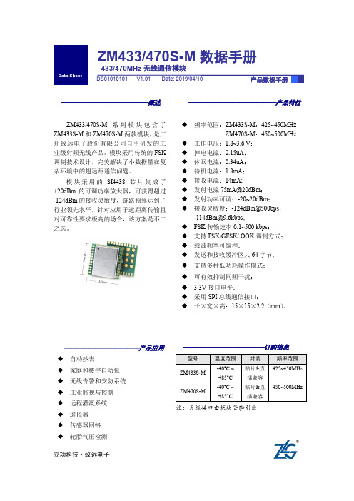
——————————————概述ZM433/470S-M 系列模块包含了ZM433S-M 和ZM470S-M 两款模块,是广州致远电子股份有限公司自主研发的工业级射频无线产品。
模块采用传统的FSK 调制技术设计,完美解决了小数据量在复杂环境中的超远距通信问题。
模块采用的SI4438芯片集成了+20dBm 的可调功率放大器,可获得超过-124dBm 的接收灵敏度,链路预算达到了行业领先水平,针对应用于远距离传输且对可靠性要求极高的场合,该方案是不二之选。
——————————————产品特性◆ 频率范围:ZM433S-M :425~450MHzZM470S-M :450~500MHz◆ 工作电压:1.8~3.6 V ; ◆ 掉电电流:0.15uA ; ◆ 休眠电流:0.34uA ; ◆ 待机电流:1.8mA ; ◆ 接收电流:14mA;◆ 发射电流75mA@20dBm ; ◆ 发射功率可调:-20~20dBm ; ◆ 接收灵敏度:-124dBm@500bps ,-114dBm@9.6kbps ;◆ FSK 传输速率0.1~500 kbps ;◆ 支持FSK/GFSK/ OOK 调制方式; ◆ 载波频率可编程;◆ 发送和接收缓冲区共64字节; ◆ 支持多种低功耗操作模式; ◆ 可有效抑制同频干扰;◆ 3.3V 接口电平;◆ 采用SPI 总线通信接口;◆ 长×宽×高:15×15×2.2(mm )。
————————————产品应用◆ 自动抄表 ◆ 家庭和楼宇自动化 ◆ 无线告警和安防系统 ◆ 工业监视与控制 ◆ 远程灌溉系统 ◆ 遥控器 ◆ 传感器网络 ◆ 轮胎气压检测ZM433/470S-M 数据手册433/470MHz 无线通信模块立功科技·致远电子修订历史目录1. 产品简介 (1)1.1产品简介 (1)1.2产品选型 (1)2. 尺寸图 (2)2.1产品尺寸 (2)2.2卷带包装 (2)3. 引脚说明 (5)3.1引脚排序 (5)3.2引脚定义 (5)4. 电气参数 (6)4.1极限参数 (7)4.2静态参数 (7)5. 射频参数 (8)6. 生产指导 (9)6.1推荐回流温度曲线 (9)7. 硬件设计注意事项 (10)7.1最小系统 (10)7.2电源设计 (10)7.3RF设计 (10)7.3.1PCB板载天线设计指导 (10)7.3.2外接天线设计指导 (11)7.3.3邮票孔天线接口设计指导 (11)7.3.4天线匹配 (13)8. 免责声明 (15)1. 产品简介1.1 产品简介ZM433/470S-M系列模块是广州致远电子股份有限公司基于Silicon Labs公司Si4438自主研发的一款工业级射频无线产品。
部分电视机CPU型号及简单代换

部分电视机CPU型号及简单代换部分电视机CPU型号及简单代换8879CPBNG6V38 海信CPU8873CPBNG6U73 创维CPUTOSHIBA-HAY-22、8873CSCNG6PR6 通用CPUTDA9373PS/N2/AI1115 SVA CPU13-TB73-TM1V001、LC863332A-5T25、LC863332A-5S97 夏华CPU88CS38N-3P48、TMP88PS38 夏华K2918、K2926,解码TB1251TDA9381PS/N3/2/1741 索尼CPUTDA9381PS/N2/3I0837 LG CPUTDA9381PS/N2/3I0975 三星CPUTDA9373PS/N2/AI0939(Haier9373-V2.0)Haier9373-V1.0 海尔CPU V1.0的可以换空白存储器,按遥控器数字8、V+ 进总线LC863324B-54M2、LC863324A-5W21、LC863324C-55M5 海信CPUOM8370-A-3NC、NOM8370-A-1NC 海信、西湖、夏华、彩星CP-2156TCL-M18V3PNICAN、TCL-M11V1P 王牌CPUH13V02-T0、8829CSNG5CJ2、H13V01-T0 TCL CPUTDA9370PS/N2/AI1429(4706-D93705-64)3P36、4P36 创维CPU 4706-D83702-64CH05T1501 长虹CHD2590M37210M3-551SP日立25M8C CPUTDA9373PS/N2/AI0911(A01V01-PH)TDA9373PS/N2/AI0996 TCL 2990UHD0401、S3F880AXZZ 创维(3S30/5S30/5S31)MN152811TJS 松下CPU 85元LC863524C-55L7、53P4、52Y7、TH-50J2 杂牌CPULC863524C-55L6、55Y5、55K8 杂牌CPU87CK38N-3647(TMP87CK38N-3675、1C48)澳柯玛、松王M37221M6-309S 厦华R2920 CPUTDA9380PS/N1/IS0380(TCL-UOC-V01)王牌CPU,用TDA9383PS代替要把60脚接地13-T00S23-03M01、8879CSBNG6K02 乐华25G6BCH08T2602(8873CSANG6JH8)长虹CPUOM8373PS/N3/2/1870(4706-D83732-64)创维短管机专用CPULC863328A-51J8 嘉华CPU8803CPAN-3PE8(8823CPNG4JR6)换存储器、39脚,C205换1UF,ST6378B1/FKF 4S02-3008 创维数码3008TMP47C434N-3526 通用王牌TCL M14VBC 王牌CPUST6367BB1/BFX 不详LC863324A-5N09 海信CPULC864512V-5C77 海信CPUM34300N4-565SPKY88C94 夏华CPUM34300N4-555SP 日立CPULC863328A-5S15 高路华、海信CPUMC8902A-5Y83 熊猫、高路华CPUMC8904A-5Z25 熊猫、高路华、海信、西湖CPUM37210M3-807SP 康力CPUT-P-16 8823CPNG5RH6 熊猫CPU SAA5647HL/M1 飞利蒲CPUOM8373PS/N3/A/1914(OM8373PS/N3/A/1854)康佳短管CPUTMP47C634AN RC18 厦华CPUHAIER1132S、HAIER1532S 海尔21T8D-S、21F9G-Shisense 8803-1(8803CPBNG3VG6)8823CPNG3PE8 海信TC2111A 换存储器、39脚,C205换1UF,OM8370PS/N3/1(HZ10V01)(TOUL 12-02M00)TCL CPUHAIER8829-V2.0(8829CPNG4PG3)海尔CPUCH0504、CH0503 长虹CPUM34302M8-612SP SONY CPUCH04T1306 长虹CPUNOM8370-A-11B 西湖CPUTCL-T00Y12-02M01(LA76931)、TOOY12-01M01 TCL CPUCKP1302S1(8829CPNG6FP6)CKP1302S 康佳CPUP88P8432N、S3C8849X13-AQB7 嘉华CPU OM8373-B-3NC 海信TF2507FLC863328C-55N6、5T45 康佳CPUTDA9373PS/N2/AI0889、4706-D93731-64 5P30 创维CPULC863328B-53P5、LC863328C-56M9、LC863328B-52E4、50J1 SVA CPUR2J10160G8-A12FP、R2J1016008-A06FP 数源S21A07 等13-TOOS13-08M01、8873CSBNG6N15 TCL CPU8873CPANG6HV9 数源TJ21A23 CPU87CM38N-1K45、87CM38N-1U87 夏华XT-259ATAVC139 三洋CPULC863320A-5N94、LC863320A-5N17(3Y01)创维CPUCH05T1604(TDA9370PS/N2/AI0848)长虹超级芯片CH05T1607(TDA9370PS/N2/AI1092)TDA9370PS 长虹超级芯片CH05T1606(TDA9373PS/N2/AI1087)TDA9373PS 长虹超级芯片CH05T1630、OM8373PS/N3/A/1842(CH05T1621)长虹,按键功能错乱,伴音失控。
ksz8851-16mll_ds芯片手册

KSZ8851-16MLL/MLLI/MLLUSingle-Port Ethernet MAC Controllerwith 8-Bit or 16-Bit Non-PCI InterfaceRevision 2.2General DescriptionThe KSZ8851M-series is a single-port controller chip witha non-PCI CPU interface and is available in 8-bit and 16-bit bus designs. This datasheet describes the 48-pin LQFPKSZ8851-16MLL for applications requiring high-performance from single-port Ethernet Controller with 8-bitor 16-bit generic processor interface. The KSZ8851-16MLL offers the most cost-effective solution for addinghigh-throughput Ethernet connectivity to traditionalembedded systems.The KSZ8851-16MLL is a single chip, mixed analog/digitaldevice offering Wake-on-LAN technology for effectivelyaddressing Fast Ethernet applications. It consists of a fastEthernet MAC controller, an 8-bit or 16-bit generic hostprocessor interface and incorporates a unique dynamicmemory pointer with 4-byte buffer boundary and a fullyutilizable 18KB for both TX (allocated 6KB) and RX(allocated 12KB) directions in host buffer interface.The KSZ8851-16MLL is designed to be fully compliant withthe appropriate IEEE 802.3 standards. An industrialtemperature-grade version of the KSZ8851-16MLLI and aqualified AEC-Q100 Automotive version of the KSZ8851-16MLLU are also available (see “Ordering Information”section).LinkMD®Physical signal transmission and reception are enhancedthrough the use of analog circuitry. This makes the designmore efficient and allows lower-power consumption. TheKSZ8851-16MLL is designed using a low-power CMOSprocess that features a single 3.3V power supply withoptions for 1.8V, 2.5V or 3.3V VDD I/O. The deviceincludes an extensive feature set that offers managementinformation base (MIB) counters and CPU control/datainterfaces with single shared data bus timing.The KSZ8851-16MLL includes a unique cable diagnosticsfeature called LinkMD®. This feature determines the lengthof the cabling plant and also ascertains if there is an openor short condition in the cable. Accompanying softwareenables the cable length and cable conditions to beconveniently displayed. In addition, the KSZ8851-16MLLsupports Hewlett Packard (HP) Auto-MDIX therebyeliminating the need to differentiate between straight orcrossover cables in applications.Functional DiagramFigure 1. KSZ8851-16MLL/MLLI Functional DiagramFeatures•Integrated MAC and PHY Ethernet Controller fully compliant with IEEE 802.3/802.3µ standards •Designed for high performance and high throughput applications•Supports 10BASE-T/100BASE-TX•Supports IEEE 802.3x full-duplex flow control and half-duplex backpressure collision flow control •Supports DMA-slave burst data read and write transfers•Supports IP Header (IPv4)/TCP/UDP/ICMP checksum generation and checking•Supports IPv6 TCP/UDP/ICMP checksum generation and checking•Automatic 32-bit CRC generation and checking •Simple SRAM-like host interface easily connects to most common embedded MCUs.•Supports multiple data frames for receive without address bus and byte-enable signals•Supports both Big- and Little-Endian processors •Larger internal memory with 12K Bytes for RX FIFO and 6K Bytes for TX FIFO. Programmable low, highand overrun watermark for flow control in RX FIFO •Shared data bus for Data, Address and Byte Enable •Efficient architecture design with configurable host interrupt schemes to minimize host CPU overhead and utilization•Powerful and flexible address filtering scheme •Optional to use external serial EEPROM configuration for MAC address•Single 25MHz reference clock for both PHY and MAC •HBM ESD Rating 6kVPower Modes, Power Supplies, and Packaging •Single 3.3V power supply with options for 1.8V, 2.5V and 3.3V VDD I/O•Built-in integrated 3.3V or 2.5V to 1.8V low noise regulator (LDO) for core and analog blocks •Enhanced power management feature with energy detect mode and soft power-down mode to ensurelow-power dissipation during device idle periodsComprehensive LED indicator support for link, activity and 10/100 speed (2 LEDs) - User programmable •Low-power CMOS design•Commercial Temperature Range: 0°C to +70°C •Industrial Temperature Range: –40°C to +85°C •Flexible package options available in 48-pin (7mm × 7mm) LQFP KSZ8851-16MLL or 128-pinPQFP KSZ8851-16/32MQLAdditional FeaturesIn addition to offering all of the features of a Layer 2 controller, the KSZ8851-16MLL offers:•Flexible 8-bit and 16-bit generic host processor interfaces with same access time and single bustiming to any I/O registers and RX/TX FIFO buffers •Supports to add two-byte before frame header in order for IP frame content with double word boundary •Micrel LinkMD® cable diagnostic capabilities to determine cable length, diagnose faulty cables, anddetermine distance to fault•Wake-on-LAN functionality– Incorporates Magic Packet™, wake-up frame, network link state, and detection of energy signaltechnology•HP Auto MDI-X™ crossover with disable/enable option •Ability to transmit and receive frames up to 2000 bytes Network Features•10BASE-T and 100BASE-TX physical layer support •Auto-negotiation: 10/100 Mbps full and half duplex •Adaptive equalizer•Baseline wander correctionApplications•Video/Audio Distribution Systems•High-end Cable, Satellite, and IP set-top boxes •Video over IP and IPTV•Voice over IP (VoIP) and Analog Telephone Adapters (ATA)•Industrial Control in Latency Critical Applications •Home Base Station with Ethernet Connection •Industrial Control Sensor Devices (Temperature, Pressure, Levels, and Valves)•Security, Motion Control and Surveillance Cameras •In-vehicle Diagnostics (OBD) & software download Markets•Fast Ethernet•Embedded Ethernet•Industrial Ethernet•Embedded Systems•Automotive EthernetOrdering InformationPart Number Temperature Range Package Lead Finish KSZ8851-16MLL 0°C to 70°C 48-Pin LQFP Pb-Free KSZ8851-16MLLI –40°C to +85°C 48-Pin LQFP Pb-Free KSZ8851-16MLLU(Automotive AEC-Q100 qualified)–40°C to +85°C 48-Pin LQFP Pb-Free KSZ8851-16MLL-Eval Evaluation Board for the KSZ8851-16MLLRevision HistoryRevision Date Summary of Changes1.0 06/30/2008 First released Information.1.1 2/13/2009 Improved EDS Rating up to 6KV, revised Ordering Information and Updated Table content and description.2.0 8/31/2009 Change revision ID from “0” to “1” in CIDER (0xc0) register. Update pins 8, 14 and 29 description for 1.8V VDD_IO supply. To add the command write (CMD=1) address index register in order for software to read back the CMD register value. To enable software read or write external EEPROM.2.104/30/2012 In 16-bit bus mode, the SD1 bit must set to “1” when CMD = 1 during DMA access. Remove auto-enqueue function, add the reset circuit. Update the description for the register PMECR Bits [1,0]. Add KSZ8851MLLU Automotive part. Add the description for the register TXCR bit 7. Update read/write timing diagram for Asynchronous Cycle. Add power sequence descriptions in the reset timing section.2.203/04/2014 Remove auto-enqueue function for transmit, Update the description for section of Asynchronous Interface. Update read/write timing diagram and table, add notes for timing table ,CIDER and RXFCTR registers. Update the defination for Register P1CR bit [9],P1MBCR bit [4] and RX/TX pair. Update the description in Half-Duplex Backpressure section. Change TTL to CMOS and updates min/max I/O voltage in different VDDIO.ContentsList of Figures (7)List of Tables (8)Pin Configuration (9)Pin Description (10)Pin for Strap-In Options (13)Functional Description (14)Functional Overview (14)Rx unused block disabled (14)Wake-up Packet (16)Physical Layer Transceiver (PHY) (17)Straight Cable (18)Crossover Cable (19)Access (21)Usage (21)Frame Queue (RXQ) Frame Format (29)EEPROM Interface (31)CPU Interface I/O Registers (33)I/O Registers (33)Internal I/O Registers Space Mapping (33)CIDER (37)0x887x (37)Reserved (38)Do Not Care (38)None (38)Register Map: MAC, PHY and QMU (39)Bit Type Definition (39)0x00 – 0x07: Reserved (39)Chip Configuration Register (0x08 – 0x09): CCR (39)0x0A – 0x0F: Reserved (39)Host MAC Address Registers: MARL, MARM and MARH (40)Host MAC Address Register Low (0x10 – 0x11): MARL (40)Host MAC Address Register Middle (0x12 – 0x13): MARM (40)Host MAC Address Register High (0x14 – 0x15): MARH (40)0x16 – 0x1F: Reserved (40)On-Chip Bus Control Register (0x20 – 0x21): OBCR (41)EEPROM Control Register (0x22 – 0x23): EEPCR (41)Memory BIST Info Register (0x24 – 0x25): MBIR (42)Global Reset Register (0x26 – 0x27): GRR (42)0x28 – 0x29: Reserved (42)Wakeup Frame Control Register (0x2A – 0x2B): WFCR (43)0x2C – 0x2F: Reserved (43)Wakeup Frame 0 CRC0 Register (0x30 – 0x31): WF0CRC0 (43)Wakeup Frame 0 CRC1 Register (0x32 – 0x33): WF0CRC1 (43)Wakeup Frame 0 Byte Mask 0 Register (0x34 – 0x35): WF0BM0 (44)Wakeup Frame 0 Byte Mask 1 Register (0x36 – 0x37): WF0BM1 (44)Wakeup Frame 0 Byte Mask 2 Register (0x38 – 0x39): WF0BM2 (44)Wakeup Frame 0 Byte Mask 3 Register (0x3A – 0x3B): WF0BM3 (44)0x3C – 0x3F: Reserved (44)Wakeup Frame 1 Byte Mask 0 Register (0x44 – 0x45): WF1BM0 (45)Wakeup Frame 1 Byte Mask 1 Register (0x46 – 0x47): WF1BM1 (45)Wakeup Frame 1 Byte Mask 2 Register (0x48 – 0x49): WF1BM2 (45)Wakeup Frame 1 Byte Mask 3 Register (0x4A – 0x4B): WF1BM3 (45)0x4C – 0x4F: Reserved (45)Wakeup Frame 2 CRC0 Register (0x50 – 0x51): WF2CRC0 (45)Wakeup Frame 2 CRC1 Register (0x52 – 0x53): WF2CRC1 (46)Wakeup Frame 2 Byte Mask 0 Register (0x54 – 0x55): WF2BM0 (46)Wakeup Frame 2 Byte Mask 1 Register (0x56 – 0x57): WF2BM1 (46)Wakeup Frame 2 Byte Mask 2 Register (0x58 – 0x59): WF2BM2 (46)Wakeup Frame 2 Byte Mask 3 Register (0x5A – 0x5B): WF2BM3 (46)0x5C – 0x5F: Reserved (46)Wakeup Frame 3 CRC0 Register (0x60 – 0x61): WF3CRC0 (46)Wakeup Frame 3 CRC1 Register (0x62 – 0x63): WF3CRC1 (47)Wakeup Frame 3 Byte Mask 0 Register (0x64 – 0x65): WF3BM0 (47)Wakeup Frame 3 Byte Mask 1 Register (0x66 – 0x67): WF3BM1 (47)Wakeup Frame 3 Byte Mask 2 Register (0x68 – 0x69): WF3BM2 (47)Wakeup Frame 3 Byte Mask 3 Register (0x6A – 0x6B): WF3BM3 (47)0x6C – 0x6F: Reserved (47)Transmit Control Register (0x70 – 0x71): TXCR (48)Transmit Status Register (0x72 – 0x73): TXSR (49)Receive Control Register 1 (0x74 – 0x75): RXCR1 (49)Receive Control Register 2 (0x76 – 0x77): RXCR2 (50)TXQ Memory Information Register (0x78 – 0x79): TXMIR (51)0x7A – 0x7B: Reserved (51)Receive Frame Header Status Register (0x7C – 0x7D): RXFHSR (51)Receive Frame Header Byte Count Register (0x7E – 0x7F): RXFHBCR (52)TXQ Command Register (0x80 – 0x81): TXQCR (52)RXQ Command Register (0x82 – 0x83): RXQCR (53)TX Frame Data Pointer Register (0x84 – 0x85): TXFDPR (54)RX Frame Data Pointer Register (0x86 – 0x87): RXFDPR (54)0x88 – 0x8B: Reserved (55)RX Duration Timer Threshold Register (0x8C – 0x8D): RXDTTR (55)RX Data Byte Count Threshold Register (0x8E – 0x8F): RXDBCTR (55)Interrupt Enable Register (0x90 – 0x91): IER (55)Interrupt Status Register (0x92 – 0x93): ISR (56)0x94 – 0x9B: Reserved (57)RX Frame Count & Threshold Register (0x9C – 0x9D): RXFCTR (57)TX Next Total Frames Size Register (0x9E – 0x9F): TXNTFSR (57)MAC Address Hash Table Register 0 (0xA0 – 0xA1): MAHTR0 (58)MAC Address Hash Table Register 1 (0xA2 – 0xA3): MAHTR1 (58)MAC Address Hash Table Register 2 (0xA4 – 0xA5): MAHTR2 (58)MAC Address Hash Table Register 3 (0xA6 – 0xA7): MAHTR3 (58)0xA8 – 0xAF: Reserved (58)Flow Control Low Watermark Register (0xB0 – 0xB1): FCLWR (58)Flow Control High Watermark Register (0xB2 – 0xB3): FCHWR (59)Flow Control Overrun Watermark Register (0xB4 – 0xB5): FCOWR (59)0xB6 – 0xBF: Reserved (59)Chip ID and Enable Register (0xC0 – 0xC1): CIDER (59)0xC2 – 0xC5: Reserved (59)0xCA – 0xCF: Reserved (60)Indirect Access Data Low Register (0xD0 – 0xD1): IADLR (60)Indirect Access Data High Register (0xD2 – 0xD3): IADHR (60)Power Management Event Control Register (0xD4 – 0xD5): PMECR (61)Go-Sleep and Wake-Up Time Register (0xD6 – 0xD7): GSWUTR (62)PHY Reset Register (0xD8 – 0xD9): PHYRR (62)0xDA – 0xDF: Reserved (62)0xE0 – 0xE3: Reserved (62)PHY 1 MII-Register Basic Control Register (0xE4 – 0xE5): P1MBCR (63)PHY 1 MII-Register Basic Status Register (0xE6 – 0xE7): P1MBSR (64)PHY 1 PHY ID Low Register (0xE8 – 0xE9): PHY1ILR (64)PHY 1 PHY ID High Register (0xEA – 0xEB): PHY1IHR (64)PHY 1 Auto-Negotiation Advertisement Register (0xEC – 0xED): P1ANAR (65)PHY 1 Auto-Negotiation Link Partner Ability Register (0xEE – 0xEF): P1ANLPR (66)0xF0 – 0xF3: Reserved (66)Port 1 PHY Special Control/Status, LinkMD (0xF4 – 0xF5): P1SCLMD (66)Port 1 Control Register (0xF6 – 0xF7): P1CR (67)Port 1 Status Register (0xF8 – 0xF9): P1SR (68)0xFA – 0xFF: Reserved (69)MIB (Management Information Base) Counters (70)Absolute Maximum Ratings (73)Operating Ratings (73)Electrical Characteristics (73)Timing Specifications (75)Asynchronous Read and Write Timing (Processor read and write) (75)Selection of Isolation Transformers (80)Selection of Reference Crystal (80)Package Information (81)Acronyms and Glossary (82)Figure 2. 48-Pin LQFP (9)Figure 3. Typical Straight Cable Connection (18)Figure 4. Typical Crossover Cable Connection (19)Figure 5. Auto Negotiation And Parallel Operation (20)Figure 6. Ksz8851-16mll 8-Bit And 16-Bit Data Bus Connections (25)Figure 8. Host Rx Single Or Multiple Frames In Auto-Dequeue Flow Diagram (30)Figure 9. Phy Port 1 Near-End (Remote) And Host Far-End (Local) Loopback Paths (32)Figure 10. Asynchronous Cycle (75)Figure 11. Auto Negotiation Timing (76)Figure 12. Reset Timing (77)Figure 13. Eeprom Read Cycle Timing Diagram (78)Figure 14. Recommended Reset Circuit (79)Figure 15. Recommended Circuit For Interfacing with Cpu/Fpga Reset (79)Table 1. Internal Function Blocks Status (14)Table 2. Mdi/Mdi-X Pin Definitions (18)Table 3. Address Filtering Scheme (23)Table 4. Bus Interface Unit Signal Grouping (24)Table 5. Frame Format For Transmit Queue (26)Table 6. Transmit Control Word Bit Fields (26)Table 7. Transmit Byte Count Format (27)Table 8. Registers Setting For Transmit Function Block (27)Table 9. Frame Format For Receive Queue (29)Table 10. Registers Setting For Receive Function Block (29)Table 11. Ksz8851-16mll Eeprom Format (31)Table 12. Format Of Mib Counters (70)Table 13. Port 1 Mib Counters Indirect Memory Offsets (71)Table 14. Asynchronous Cycle Timing Parameters (75)Table 15. Auto Negotiation Timing Parameters (76)Table 16. Reset Timing Parameters (77)Table 17. Eeprom Timing Parameters (78)Table 18. Transformer Selection Criteria (80)Table 19. Qualified Single Port Magnetics (80)Table 20. Typical Reference Crystal Characteristics (80)Figure 2. 48-Pin LQFPPin Number Pin Name Type Pin Function1 P1LED1 IPU/O Programmable LED output to indicate port activity/status.LED is ON when output is LOW; LED is OFF when output is HIGH.Port 1 LED indicators1 defined as follows:Chip Global Control Register: CGCR bit [9]0 (Default) 1P1LED1 100BT ACTP1LED0 LINK/ACT LINK1. Link = LED On; Activity = LED Blink; Link/Act = LED On/Blink;Speed = LED On (100BASE-T); LED Off (10BASE-T)Config Mode: The P1LED1 pull-up/pull-down value is latched as 16/8-bit mode during power-up / reset. See “Strapping Options” section for details2 P1LED0 OPU3 PME OPU Power Management Event (default active low): It is asserted (low or high depends on polarity set in PMECR register) when one of the wake-on-LAN events is detected by KSZ8851-16MLL. The KSZ8851-16MLL is requesting the system to wake up from low power mode.4 INTRN OPU Interrupt: An active low signal to host CPU to indicate an interrupt status bit is set, this pin need an external 4.7K pull-up resistor.5 RDN IPU Read Strobe NotAsynchronous read strobe, active low to indicate read cycle.6 WRN IPU Write Strobe NotAsynchronous write strobe, active low to indicate write cycle.7 DGND GND Digital ground8 VDD_CO1.8 P 1.8V regulator output . This 1.8V output pin provides power to pins 14 (VDD_A1.8) and 29 (VDD_D1.8) for core VDD supply.If VDD_IO is set for 1.8V then this pin should be left floating, pins 14 (VDD_A1.8) and 29 (VDD_D1.8) will be sourced by the external 1.8V supply that is tied to pins 27, 38 and 46 (VDD_IO) with appropriate filtering.9 EED_IO IPD/O In/Out Data from/to external EEPROM.Config Mode: The pull-up/pull-down value is latched as with/without EEPROM during power-up / reset. See “Strapping Options” section for details10 EESK IPD/O EEPROM Serial ClockA 4µs (OBCR[1:0]=11 on-chip bus speed @ 25MHz) or 800ns (OBCR[1:0]=00 on-chip bus speed @ 125MHz) serial output clock cycle to load configuration data from the serial EEPROM.Config Mode: The pull-up/pull-down value is latched as big/little endian mode during power-up / reset. See “Strapping Options” section for details11 CMD IPD Command TypeThis command input decides the SD[15:0] shared data bus access information.When command input is low, the access of shared data bus is for data access in 16-bit mode shared data bus SD[15:0] or in 8-bit mode shared data bus SD[7:0].When command input is high, the access of shared data bus is for address A[7:2] access at shared data bus SD[7:2], byte enable BE[3:0] at SD[15:12] and the SD[11:8] is “Do Not Care” in 16-bit mode. It is for address A[7:0] access at SD[7:0] in 8-bit mode.Pin Number Pin Name Type Pin Function12 CSN IPU Chip Select NotChip select for the shared data bus access enable, active Low.13 AGND GND Analog ground14 VDD_A1.8 P 1.8V analog power supply from VDD_CO1.8 (pin 8) with appropriate filtering. If VDD_IO is 1.8V, this pin must be supplied power from the same source as pins 27, 38 and 46 (VDD_IO) with appropriate filtering.15 EECS OPD EEPROM Chip SelectThis signal is used to select an external EEPROM device.16 RXP1 I/O Port 1 physical receive signal (+ differential).17 RXM1 I/O Port 1 physical receive signal (– differential).18 AGND GND Analog ground.19 TXP1 I/O Port 1 physical transmit signal (+ differential).20 TXM1 I/O Port 1 physical transmit signal (– differential).21 VDD_A3.3 P 3.3V analog VDD input power supply with well decoupling capacitors.22 ISET O Set physical transmits output current.Pull-down this pin with a 3.01K 1% resistor to ground.23 RSTN IPU Reset NotHardware reset pin (active Low). This reset input is required minimum of 10ms low after stable supply voltage 3.3V.24 X1 I 25MHz crystal or oscillator clock connection.Pins (X1, X2) connect to a crystal. If an oscillator is used, X1 connects to a 3.3V tolerant oscillator and X2 is a no connect.Note: Clock requirement is ±50ppm for either crystal or oscillator.25 X2 O26 DGND GND Digital ground27 VDD_IO P 3.3V, 2.5V or 1.8V digital VDD input power supply for IO with well decoupling capacitors.28 DGND GND Digital ground29 VDD_D1.8 P 1.8V digital power supply from VDD_CO1.8 (pin 8) with appropriate filtering. If VDD_IO is 1.8V, this pin must be supplied power from the same source as pins 27, 38 and 46 (VDD_IO) with appropriate filtering.30 SD15 I/O (PD) Shared Data Bus bit 15. Data D15 access when CMD=0. Byte Enable 3 at double-word boundary access (BE3, 4th byte enable and active high) in 16-bit mode when CMD=1. This pin must be tied to GND in 8-bit bus mode.31 SD14 I/O (PD) Shared Data Bus bit 14. Data D14 access when CMD=0. Byte Enable 2 at double-word boundary access (BE2, 3rd byte enable and active high) in 16-bit mode when CMD=1. This pin must be tied to GND in 8-bit bus mode.32 SD13 I/O (PD) Shared Data Bus bit 13. Data D13 access when CMD=0. Byte Enable 1 at double-word boundary access (BE1, 2nd byte enable and active high) in 16-bit mode when CMD=1. This pin must be tied to GND in 8-bit bus mode.33 SD12 I/O (PD) Shared Data Bus bit 12. Data D12 access when CMD=0. Byte Enable 0 at double-word boundary access (BE0, 1st byte enable and active high) in 16-bit mode when CMD=1. This pin must be tied to GND in 8-bit bus mode.34 SD11 I/O (PD) Shared Data Bus bit 11. Data D11 access when CMD=0. Do Not Care when CMD=1. This pin must be tied to GND in 8-bit bus mode.35 SD10 I/O (PD) Shared Data Bus bit 10. Data D10 access when CMD=0. Do Not Care when CMD=1. This pin must be tied to GND in 8-bit bus mode.Pin Number Pin Name Type Pin Function36 SD9 I/O (PD) Shared Data Bus bit 9. Data D9 access when CMD=0. Do Not Care when CMD=1. This pin must be tied to GND in 8-bit bus mode.37 DGND GND Digital ground38 VDD_IO P 3.3V, 2.5V or 1.8V digital VDD input power supply for IO with well decoupling capacitors.39 SD8 I/O (PD) Shared Data Bus bit 8. Data D8 access when CMD=0. Do Not Care when CMD=1. This pin must be tied to GND in 8-bit bus mode.40 SD7 I/O (PD) Shared Data Bus bit 7. Data D7 access when CMD=0. Address A7 access when CMD=1.41 SD6 I/O (PD) Shared Data Bus bit 6. Data D6 access when CMD=0. Address A6 access when CMD=1.42 SD5 I/O (PD) Shared Data Bus bit 5. Data D5 access when CMD=0. Address A5 access when CMD=1.43 SD4 I/O (PD) Shared Data Bus bit 4. Data D4 access when CMD=0. Address A4 access when CMD=1.44 SD3 I/O (PD) Shared Data Bus bit 3. Data D3 access when CMD=0. Address A3 access when CMD=1.45 SD2 I/O (PD) Shared Data Bus bit 2. Data D2 access when CMD=0. Address A2 access when CMD=1.46 VDD_IO P 3.3V, 2.5V or 1.8V digital VDD input power supply for IO with well decoupling capacitors.47 SD1 I/O (PD) Shared Data Bus bit 1. Data D1 access when CMD=0. In 8-bit mode, this is address A1 access when CMD=1. In 16-bit mode, this is “Do Not Care” when CMD=1.48 SD0 I/O (PD) Shared Data Bus bit 0. Data D0 access when CMD=0. In 8-bit mode, this is address A0 access when CMD=1. In 16-bit mode, this is “Do Not Care” when CMD=1.Legend:P = Power supplyGND = GroundI/O = Bi-directionalI = InputO = Output.IPD = Input with internal pull-down (58K ±30%).IPU = Input with internal pull-up (58K ±30%).OPD = Output with internal pull-down (58K ±30%).OPU = Output with internal pull-up (58K ±30%).IPU/O = Input with internal pull-up (58K ±30%) during power-up/reset; output pin otherwise. IPD/O = Input with internal pull-down (58K ±30%) during power-up/reset; output pin otherwise. I/O (PD) = Input/Output with internal pull-down (58K ±30%).Pin for Strap-In OptionsPin Number Pin Name Type Pin Function1 P1LED1 IPU/O 8 or 16-bit bus mode select during power-up / reset: NC or Pull-up (default ) = 16-bit busPull-down = 8-bit busThis pin value is also latched into register CCR, bit 6/7.9 EED_IO IPD/O EEPROM select during power-up / reset:Pull-up = EEPROM presentNC or Pull-down (default ) = EEPROM not present This pin value is latched into register CCR, bit 9.10 EESK IPD/O Endian mode select during power-up / reset:Pull-up = Big EndianNC or Pull-down (default) = Little EndianThis pin value is latched into register CCR, bit 10.When this pin is no connect or tied to GND, the bit 11 (Endian mode selection) in RXFDPR register can be used to program either Little (bit11=0 default) Endian mode or Big (bit11=1) Endian mode.Note: IPU/O = Input with internal pull-up (58K ±30%) during power-up/reset; output pin otherwise.IPD/O = Input with internal pull-down (58K ±30%) during power-up/reset; output pin otherwise.Pin strap-ins are latched during power-up or reset.Functional DescriptionThe KSZ8851-16MLL is a single-chip Fast Ethernet MAC/PHY controller consisting of a 10/100 physical layer transceiver (PHY), a MAC, and a Bus Interface Unit (BIU) that controls the KSZ8851-16MLL via an 8-bit or 16-bit host bus interface. The KSZ8851-16MLL is fully compliant to IEEE802.3u standards.Functional OverviewPower ManagementThe KSZ8851-16MLL supports enhanced power management feature in low power state with energy detection to ensure low-power dissipation during device idle periods. There are four operation modes under the power management function which is controlled by two bits in PMECR (0xD4) register as shown below:PMECR[1:0] = 00 Normal Operation ModePMECR[1:0] = 01 Energy Detect ModePMECR[1:0] = 10 Soft Power-down modePMECR[1:0] = 11 Power-saving modeTable 1 indicates all internal function blocks status under four different power management operation modes.KSZ8851-16MLL Function BlocksPower Management Operation ModesNormal Mode Power-saving mode Energy Detect Mode Soft Power-Down ModeInternal PLL Clock Enabled Enabled Disabled DisabledTx/Rx PHY Enabled Rx unused block disabled Energy detect at Rx DisabledMAC Enabled Enabled Disabled DisabledHost Interface Enabled Enabled Disabled DisabledTable 1. Internal Function Blocks StatusNormal Operation ModeThis is the default setting bit[1:0]=00 in PMECR register after the chip power-up or hardware reset (pin 67). When KSZ8851-16MLL is in this normal operation mode, all PLL clocks are running, PHY and MAC are on and the host interface is ready for CPU read or write.During the normal operation mode, the host CPU can set the bit[1:0] in PMECR register to transit the current normal operation mode to any one of the other three power management operation modes.Energy Detect ModeThe energy detect mode provides a mechanism to save more power than in the normal operation mode when the KSZ8851-16MLL is not connected to an active link partner. For example, if cable is not present or it is connected to a powered down partner, the KSZ8851-16MLL can automatically enter to the low power state in energy detect mode. Once activity resumes due to plugging a cable or attempting by the far end to establish link, the KSZ8851-16MLL can automatically power up to normal power state in energy detect mode.Energy detect mode consists of two states, normal power state and low power state. While in low power state, the KSZ8851-16MLL reduces power consumption by disabling all circuitry except the energy detect circuitry of the receiver. The energy detect mode is entered by setting bit[1:0]=01 in PMECR register. When the KSZ8851-16MLL is in this mode, it will monitor the cable energy. If there is no energy on the cable for a time longer than pre-configured value at bit[7:0] Go-Sleep time in GSWUTR register, KSZ8851-16MLL will go into a low power state. When KSZ8851-16MLL is in low power state, it will keep monitoring the cable energy. Once the energy is detected from the cable and is continuously presented for a time longer than pre-configured value at bit[15:8] Wake-Up time in GSWUTR register, the KSZ8851-16MLL will enter either the normal power state if the auto-wakeup enable bit[7] is set in PMECR register or the normal operation mode if both auto-wakeup enable bit[7] and wakeup to normal operation mode bit[6] are set in PMECR register.The KSZ8851-16MLL will also assert PME output pin if the corresponding enable bit[8] is set in PMECR (0xD4) register or generate interrupt to signal an energy detect event occurred if the corresponding enable bit[2] is set in IER (0x90) register. Once the power management unit detects the PME output asserted or interrupt active, it will power up the host CPU and issue a wakeup command which is a read cycle to read the Globe Reset Register (GRR at 0x26) to wake up the KSZ8851-16MLL from the low power state to the normal power state in case the auto-wakeup enable bit[7] is disabled. When KSZ8851-16MLL is at normal power state, it is able to transmit or receive packet from the cable.Soft Power-Down ModeThe soft power-down mode is entered by setting bit[1:0]=10 in PMECR register. When KSZ8851-16MLL is in this mode, all PLL clocks are disabled, the PHY and the MAC are off, all internal registers value will not change, and the host interface is only used to wake-up this device from current soft power-down mode to normal operation mode.In order to go back the normal operation mode from this soft power-down mode, the only way to leave this mode is through a host wake-up command which the CPU issues to read the Globe Reset Register (GRR at 0x26).Power-Saving ModeThe power-saving mode is entered when auto-negotiation mode is enabled, cable is disconnected, and by setting bit[1:0]=11 in PMECR register and bit [10]=1 in P1SCLMD register. When KSZ8851M is in this mode, all PLL clocks are enabled, MAC is on, all internal registers value will not change, and host interface is ready for CPU read or write. In this mode, it mainly controls the PHY transceiver on or off based on line status to achieve power saving. The PHY remains transmitting and only turns off the unused receiver block. Once activity resumes due to plugging a cable or attempting by the far end to establish link, the KSZ8851M can automatically enabled the PHY power up to normal power state from power-saving mode.During this power-saving mode, the host CPU can program the bit[1:0] in PMECR register and set bit[10]=0 in P1SCLMD register to transit the current power-saving mode to any one of the other three power management operation modes. Wake-on-LANWake-up frame events are used to wake the system whenever meaningful data is presented to the system over the network. Examples of meaningful data include the reception of a Magic Packet, a management request from a remote administrator, or simply network traffic directly targeted to the local system. In all of these instances, the network device is pre-programmed by the policy owner or other software with information on how to identify wake frames from other network traffic. The KSZ8851-16MLL controller can be programmed to notify the host of the wake-up frame detection with the assertion of the interrupt signal (INTRN) or assertion of the power management event signal (PME).A wake-up event is a request for hardware and/or software external to the network device to put the system into a powered state (working).A wake-up signal is caused by:1. Detection of energy signal over a pre-configured value (bit 2 in ISR register)2. Detection of a linkup in the network link state (bit 3 in ISR register)3. Receipt of a Magic Packet (bit 4 in ISR register)4. Receipt of a network wake-up frame (bit 5 in ISR register)There are also other types of wake-up events that are not listed here as manufacturers may choose to implement these in their own way.Detection of EnergyThe energy is detected from the cable and is continuously presented for a time longer than pre-configured value, especially when this energy change may impact the level at which the system should re-enter to the normal power state. Detection of LinkupLink status wake events are useful to indicate a linkup in the network’s connectivity status.。
OKI烙铁头型号表

OKI烙铁头型号表STTC系列烙铁头STTC系列烙铁头用于MX系列主机上,该烙铁头不能用于SP200系统,也不能用于镊型手柄和除锡手柄. 最常用的STTC烙铁头型号STTC-X37 凿型,横刃STTC-X36* 凿型,横刃形形30?,1.5mm(0.1″)30?,1.78mm(0.07″)多种用途烙铁头,如果是初次使用Metcal烙铁,建议选用于较长烙铁头的中到大的焊点用STTC-037STTC-X38* 凿型,横刃STTC- X25 凿型,横刃形形30?,1.5mm(0.053″) 30?,1.0mm(0.04″) 较STTC-037细.适用于中小焊点的通孔焊接和一般的表适合各种小焊点的焊接,STTC-025可作为SMT焊接的首面贴焊接选烙铁头STTC-X07 尖锥STTC-X22 尖锥型,1.0mm(0.04″) 型,0.4mm(0.016″)在焊接空间有限时的通用SMT和通孔焊接烙铁头适用于SMT器件和细线的焊接工作(不适用于通孔焊接)STTC-X06 尖锥STTC-X40 弯曲尖头型,0.4mm(0.016″) 30?,0.4mm(0.016″)适合焊接SMT器件,弯头使小电路板和PLCC器件的焊接用于焊接空间有限的SMT返修更加容易STTC-X45 斜面60?,0.4mm(0.016″) X-表示温度系列:X=5为500系列,X=0为600系列,X=1 为700系列,X=8为800系列为加长的尖细烙铁头,适用于SMT器件和细线的焊接工作(不适用于通孔焊接)温度500系列=5,600系列X=0,700系列,1,800系列X=8(带*)温度系列规格无铅应用华氏温度/摄氏温度500 STTC-5XX 温度敏感 575?/302?600 STTC-0XX 温度敏感 675?/357?700 STTC-1XX 玻璃纤维 775?/412?800 STTC-8XX 陶瓷 905?/487?其他的标准的STTC烙铁头型号STTC-X17* 特大凿STTC-X65 大凿形,5.0mm(0.2″) 形,5.0mm(0.2″)STTC-X20 加长凿形STTC-X03* 凿形12?,3.8mm(0.15″) 90?,3.0mm(0.12″)STTC-X13 凿形STTC-X33 凿形90?,3.0mm(0.07″) 90?,2.5m(0.10″)STTC-X04 凿形STTC-X42 加长凿形90?,1.78mm(0.07″60?,1.78(0.07″) )STTC-X98 弯曲凿型STTC-X99 弯曲凿型30?,1.78mm(0.07″30?,1.5m(0.47″) )STTC-X41 长头凿形STTC-X83 长头开槽30?,1.3mm(0.05″) 型,2.0m(0.08″)STTC-X32 尖锥STTC-X02 尖锥形,1.78mm(0.07″) 形,1.78mm(0.07″)STTC-X01 尖锥STTC-X31尖锥形,1.0mm(0.04″) 形,1.0m(0.04″)STTC-X43 尖锥STTC-X12 锥形,0.5mm(0.02″) 形,2.03mm(0.08″)STTC-X11 锥STTC-X16 锥形,0.5mm(0.02″) 形,0.5mm(0.02″)STTC-X44 尖弯STTC-X26 尖弯30?,0.5mm(0.02″) 30?,0.4mm(0.16″)STTC-X14 斜面STTC-X35 斜面45?,2.03mm(0.08″30?,1.78mm(0.07″) )STTC-X47 斜面STTC-X05 斜面60?,1.78mm(0.07″30?,1.78mm(0.07″) )STTC-X15, 斜面型STTC-X24, 斜面型30?,1.3mm(0.05″) 30 ?,1.0mm(0.04″)STTC-X97, 前上端开STTC-X70, 前端异槽,5.3mm(0.21″) 性,4.8mm(0.19″)STTC-X46, 斜面型STTC-X90 圆锥60?,1.0mm(0.04″) 形,0.25mm(0.01″)STTC-X14 倾斜形STTC-X45P 圆锥45?,2mm(0.08″) 形,0.4mm(0.016″)STTC-X01P圆锥STTC-X25P横刃形形,1mm(0.04″) 30?,1mm(0.04″)STTC-X38P横刃形STTC-X37P横刃形30?,1.5mm(0.06″) 30?,1.78mm(0.07″)STTC-X47P倾斜型STTC-X36P横刃形60?,1.78mm(0.07″30?,2.5mm(0.1″))STTC-X173P刀形,5mm(0.2″)温度500系列X=5,600系列=0,700系列X,1,800系列X=8(带*)温度系列规格无铅应用华氏温度/摄氏温度500 STTC-5XX 温度敏感 575?/302?600 STTC-0XX 温度敏感 675?/357?700 STTC-1XX 玻璃纤维 775?/412?800 STTC-8XX 陶瓷 905?/487?SMTC系列烙铁头我们还提供SMTC烙铁头,帮助您完成焊接,起拔芯片与清理焊盘的工作.她的形状有槽形,隧道形和方形.此外,SMTC烙铁头还有其他形状的烙铁头,如,马蹄形,用于托焊;扁铲形,用于清理焊盘;刀形,用于空间狭小的PLCC管脚焊-RM3E标准手柄,不能用于镊形手柄,除锡手柄和SP200,PS800系统. 接.SMTC烙铁头只用于MX槽型烙铁头SMT元件烙铁头尺寸(mm)编号 A B D 烙铁头型号 Chip0805 2.29 1.27 1.79 SMTC-X01 Chip1206,1210 3.56 1.52 1.79 SMTC-X02 Chip1808,1812 4.83 2.03 1.91 SMTC-X03Chip,BoxA(EIASOPM-3224) 3.43 2.03 3.05 SMTC-X35 Chip,BoxB(EIASOPM-3528) 3.81 2.41 2.54 SMTC-X32 Melf,BoxB(EIASOPM-4532) 4.83 2.79 4.06 SMTC-X36 Chip,BoxC(EIASOPM-6032) 6.35 2.41 3.30 SMTC-X33* Chip,BoxD(EIASOPM-7246) 7.62 2.54 3.56 SMTC-X34* SOT-23 1.73 2.54 1.27 SMTC-X05 SOT-89 2.80 6.35 2.03 SMTC-X08 Chip0402,0603,0805(angled) 2.03 1.27 1.52 SMTC-X88Chip0402,0603 1.78 1.02 1.02 SMTC-X96 温度500系列X=5, 600系列X=0, 700系列X=1, *:无500系列. 温度系列规格无铅应用华氏温度/摄氏温度 500 SMTC-5XX 温度敏感 575?/302?600 SMTC-0XX 温度敏感 675?/357?700 SMTC-1XX 玻璃纤维 775?/412?800 SMTC-8XX 陶瓷 905?/487?隧道型烙铁头适用于双排管脚元件SMT元件内部尺寸(mm)编号 A2 A B D 烙铁头型号 DPAC 8.51 8.51 6.35 5.08 SMTC-X47 SO-8 8.13 9.65 19.05 6.10 SMTC-X107 SO-16 8.38 8.38 12.07 5.84 SMTC-X46* SO-8 8.51 8.51 16.90 6.35 SMTC-X68** SOIC-8 5.08 5.08 4032 2.29 SMTC-X04 SOIC-14,-16 5.08 5.08 10.16 2.29 SMTC-X06 SOIC-14 5.18 5.18 8.89 2.54 SMTC-X142 SOIC-24(Mini flat pack) 7.11 7.11 15.75 3.18 SMTC-X77 SOIC-16(Wide) 8.138.13 11.94 6.86 SMTC-X124 SOIC-20 9.53 9.53 13.21 3.18 SMTC-X10 SOIC-249.53 9.53 15.75 3.18 SMTC-X09 SOIC-28,SOL-36 9.53 9.53 18.29 3.18 SMTC-X07 SOIC-32 13.21 13.21 20.45 4.32 SMTC-X42 SOJ-28,SOM-36 8.00 8.6418.80 1.88 SMTC-X26 SOJ-32,34 8.00 8.64 21.34 3.18 SMTC-X140 SOJ-40,SOM-32 10.41 11.43 25.91 1.91 SMTC-X40 SOJ-42 10.41 11.43 27.18 3.18 SMTC-X148 SOMC-14,-16,DB-20 6.86 6.86 11.18 2.29 SMTC-X20 SOP-20 6.86 6.86 7.24 2.54 SMTC-X138 SOP-28 10.67 10.67 18.29 3.18 SMTC-X39 SOP-40 11.68 12.95 25.4 3.18 SMTC-X134* SOP-44 12.95 14.35 27.18 2.67 SMTC-X83 TSOP-28 11.94 12.83 8.13 1.65 SMTC-X95 TSOP-40 18.54 19.30 10.16 3.05 SMTC-X154 TSOP-56 18.54 19.30 14.12 3.05 SMTC-X62 TSOP-32 18.51 19.30 8.13 3.05 SMTC-X84** 温度600系列X=0,700系列X=1,*:无600系列,**:无700系列. 温度系列规格无铅应用华氏温度/摄氏温度 500 SMTC-5XX 温度敏感 575?/302? 600 SMTC-0XX 温度敏感 675?/357? 700 SMTC-1XX 玻璃纤维 775?/412? 800 SMTC-8XX 陶瓷 905?/487?方形烙铁头用于PLCC元件SMT元件内部尺寸(mm)编号 A2 A B2 B D 烙铁头型号 PICC18 7.62 8.38 12.70 13.46 3.81 SMTC-X11 PICC20 9.14 10.16 9.14 10.16 3.81 SMTC-X12 PICC28 9.40 10.41 14.48 15.49 3.81 SMTC-X103 PICC32 11.43 12.70 13.97 15.24 3.81 SMTC-X16 PICC28 11.56 12.70 11.58 12.70 3.81 SMTC-X13 PICC44 16.76 12.78 16.76 17.783.81 SMTC-X14 PICC68 24.38 25.27 24.38 25.27 5.59 SMTC-X18* PICC68双主机 24.38 25.27 24.38 25.27 5.59 SMTC-X28 PICC84双主机 29.59 30.35 29.59 30.35 5.59 SMTC-X29 PICC52 19.30 20.32 19.30 20.32 3.81 SMTC-X17* PICC84 29.59 30.35 29.59 30.35 5.59 SMTC-X19* 温度600系列X=0,700系列X=1,所有方形元件推荐用700系列.*:无600系列.注:双主机系列需要二个手柄MX-RM3E和一个MX-DHS(建议使用) 温度系列规格无铅应用华氏温度/摄氏温度 500 SMTC-5XX 温度敏感 575?/302? 600 SMTC-0XX 温度敏感 675?/357? 700 SMTC-1XX 玻璃纤维 775?/412? 800 SMTC-8XX 陶瓷905?/487?方形烙铁头用于QFP元件SMT元件内部尺寸(mm)编号 A2 A B2 B D 烙铁头型号 SQFP48(EIAJ) 8.38 8.38 8.38 8.38 2.54 SMTC-X121 SQFP64(EIAJ) 11.18 11.18 11.18 11.18 2.54 SMTC-X120 TQFP4411.18 12.19 12.19 13.21 2.79 SMTC-X159 TQFP80 12.32 13.34 12.32 13.342.79 SMTC-X132 QFP48 13.97 13.97 13.97 13.97 3.30 SMTC-X115 VQFP100(EIAJ) 14.48 15.49 14.48 15.49 2.79 SMTC-X118 VQFP128(3.2mmfp) 15.75 15.7521.84 21.84 3.30 SMTC-X133 QFP44 16.13 16.13 16.13 16.13 3.30 SMTC-X21 QFP100(长方形) 16.51 16.51 22.48 22.48 3.30 SMTC-X43 QFP64,80 17.1517.15 23.11 23.11 3.30 SMTC-X15 QFP100 20.45 20.45 20.45 20.45 4.83 SMTC-X45* QFP144 20.45 21.34 20.45 21.34 1091 SMTC-X122 QFP132 25.0225.91 25.02 25.91 3.18 SMTC-X86 QFP100(方形) 26.42 26.42 26.42 26.423.30 SMTC-X44* QFP208(双主机) 28.58 44.96 28.58 44.96 2.90 SMTC-X81QFP120,160(双主机) 29.59 30.48 29.59 30.48 3.05 SMTC-X48 PQFP240()双主机32.77 33.78 32.77 33.78 2.79 SMTC-X125 QFP304(双主机) 40.64 41.91 41.91 40.64 5.08 SMTC-X158** 温度600系列X=0,700系列X=1,所有方形烙铁头建议使用700系列. *:不推荐用600系列;**:无600系列注:双主机系列需要二个手柄MX-RM3E和一个MX-DHS(建议使用). 温度系列规格无铅应用华氏温度/摄氏温度 500 SMTC-5XX 温度敏感 575?/302? 600 SMTC-0XX 温度敏感 675?/357? 700 SMTC-1XX 玻璃纤维 775?/412? 800 SMTC-8XX 陶瓷905?/487?方形烙铁头用于起拔PLCC元件插座SMD元件型号 A B D 烙铁头型号推荐烙铁头型号 PLCC-20SOCKET 9.14 9.14 2.91 SMTC-X144 SMTC-1144 PLCC-32SOCKET 11.58 14.12 3.05 SMTC-X109 SMTC-1109 PLCC-84SOCKET* 40.64 40.64 2.91 SMTC-X145 SMTC-1145 温度600系列X=0,700系列X=1,建议使用700系列 *:双主机系列需要二个手柄MX-RM3E和一个MX-DHS(建议使用) 温度系列规格无铅应用华氏温度/摄氏温度 500 SMTC-5XX 温度敏感 575?/302?600 SMTC-0XX 温度敏感 675?/357?700 SMTC-1XX 玻璃纤维 775?/412?800 SMTC-8XX 陶瓷 905?/487?用于MX系统的SMTC特殊形状烙铁头,用于焊盘清理使用Metcal的扁铲形烙铁头和铜编带配合使用可以清理两面和四面引脚芯片的焊盘,方便、快捷并且非常安全.在清理焊盘时请特别注意,不要用烙铁头和铜编带在焊盘来回拖动,这样会造成焊盘脱落.扁铲形烙铁头SMTC-X110* 扁铲形 SMTC-X62 扁铲形 SMTC-X61 扁铲形 SMTC-X60 扁铲形头宽39.37mm 头宽22.10mm 头宽15.75mm 头宽10.41mm温度500系列X=5,600系列X=0,700系列X=1,800系列X=8. *不提供500、800系列,双主机蹄形和刀形烙铁头,用于拖焊图示型号图示型号SMTC-X167**小蹄SMTC-X147* 蹄形形SMTC-X169*长蹄SMTC-X170*长蹄形形SMTC-X161*刀形, SMTC-X173刀形,涂锡面2.03mm 涂锡面5.84mm温度500系列X=5, 600系列X=0, 700系列X=1, 800系列X=8*无800系列, **无500、800系列其余SMTC特殊形状烙铁头SMTC-X98** SMTC-X100 SMTC-X136** 28针SMT连接头微型XMT头热板形烙铁头温度500系列X=5,600系列X=0,700系列X=1,800系列X=8 **:无500系列,800系列刀片形烙铁头刀片形烙铁头专门用于有效而快速的清洁PCB焊盘.MX-2010系统为此类刀片形烙铁头提供了充足的能量.Metal的TMSmartHeat技术可以确保极其迅速地响应负载要求,实现真正无风险的焊盘清洁过程. 图示型号图示型号SMTC-X64刀片形SMTC-X60刀片形5mm(0.2″) 10mm(0.4″)SMTC-X61刀片形SMTC-X62刀片形15.75mm(0.62″) 22mm(0.86″)SMTC-X63双加热器,刀片形45.46mm(1.79″)SMTC微型烙铁头微型烙铁头适用于间距很小的微型芯片.这种烙铁头既可以从用于拆除0402,0201微小元件,也可以用于微型的PLCC,QFP元件管脚上面的拖焊.您可以根据以下尺寸选择适合的型号:图示型号SMTC-X171适用于拆除0201,0402微型元件,因为弯头,便于观测和拆除.SMTC-X172适用于微细管脚拖焊和点对点的焊接,且便于清理连焊SMTC-X174适用于比小蹄型还小的密管脚处的拖焊SMTC-X175适用于比小蹄型还小的密管脚处的拖焊SMTC-X90适用于0201 ,0402微型元件精细焊接温度500系列 X=5,600系列X=0,700系列X=1,800系列X=8.温度系列规格无铅应用华氏温度/摄氏温度500 SMTC-5XX 温度敏感 575?/302?600 SMTC-0XX 温度敏感 675?/357?700 SMTC-1XX 玻璃纤维 775?/412?800 SMTC-8XX 陶瓷 905?/487?STDC除锡烙铁头(用于MX-5050和MX-500DS除锡系统) 应从下面的STDC系列烙铁头中选购最适合您的型号.它有两种供您选择:标准型和加长型.和所有OK烙铁头一样,更换STDC烙铁头,只需要几秒钟,非常方便.正确选择该烙铁头的型号和温度,对于有效完成通孔除锡十分重要.标准型STDC烙铁头型号与尺寸(mm)型号内径A(mm) 内径B(mm) STDC-X02 0.64 1.40STDC-X03 0.76 1.68STDC-X04 1.02 1.78STDC-X05 1.27 2.03STDC-X06 1.52 2.29STDC-X07 2.41 3.18温度 600系列X=0 700系列X=1 800系列X=8加长型STDC烙铁头型号与尺寸(mm)型号内径A 内径BSTDC-X03L 0.76 1.68STDC-X04L 1.02 1.79STDC-X05L 1.27 2.03温度700系列X=7 800系列X=8选择正确的温度(系列)STDC烙铁头寿命特别长,并且设计为用于传递高热量,使多层电路板的除锡轻而易举。
- 1、下载文档前请自行甄别文档内容的完整性,平台不提供额外的编辑、内容补充、找答案等附加服务。
- 2、"仅部分预览"的文档,不可在线预览部分如存在完整性等问题,可反馈申请退款(可完整预览的文档不适用该条件!)。
- 3、如文档侵犯您的权益,请联系客服反馈,我们会尽快为您处理(人工客服工作时间:9:00-18:30)。
5
4
3
2
1
Version
Date
Author
Change Note
Note
V1.0 V1.1
20130504 20130522
LVJQ LVJQ
First edictor 1: Change The ESD Component with Low capacitance(U143:ESDA6V8UD/AZC199-02S)In the USB port 2: Increase a pull-up resistor(R473:10K) to pin16 of the ACT8846QM460
C
RK3188
USB OTG2.0 USB HOST2.0
3G MODULE
GPS Demod OSC 24M 32K CLKIN
RESET IR IN GPIO &AD
B
B
DC JACK 5V/2A
PWR Supply
CHARGE& POWERSWITCH PMIC BATTRY DETECTOR Coulomb IC RESET
D
D
C
C
B
B
A
A
福州瑞芯微电子有限公司
Title:
Modify note
REV: 1.1 Page Num: 2 Page Total: 17
1
File: RK3188_Ref_HDMI_1CELL
Create Date: Friday, January 18, 2013 Modify Date:
5 4 3 2
ISET 1.5A 2A
6
7
8
ILIM=1.15*40000/R105(mA) ILIM
3 Q34 8050 SOT23 H19 H500X250
R29 100K 1 R0402 R152 CHG_VCC 10K R0402
1
1
1
1
2
H14 H500X250
H15 H500X250
H16 H500X250
REV: 1.1 Page Num: 4 Page Total:17
1
File: RK3188_Ref_HDMI_1CELL
Create Date: Modify Date:
Friday, January 18, 2013 Tuesday, August 13, 2013
5
4
3
2
1
1
T23 TEST T-1.0 T22 TEST T-1.0 DC5V VBUS0
DDR Interface
HSADC SDIO0 SDIO1 UART0
WIFI+BT+GPS+FM RK903 WIFI+BT+FM
LVDS PANEL
LVDS IC
LCDC1
HSIC
C
Audio output
I2S CODEC I2C DEVICE TOUCH PANEL& LIGHT SENSOR DEBUG I2C4 I2C0 I2C2 UART2 I2C1
Camera _1.8V
REG8 INL2 REG9
OUT8
VCCA_33
CODEC
OUT9
VCC_TP
TOUCH PANEL
REG10 INL3
B
OUT10
VCCIO_WL
WIFI
REG11
OUT11
VCC_18
WIFI/FLASH IO USB_PHY_1.8V RK3188_SAR-ADC_1.8V
Tuesday, August 13, 2013
5
4
3
2
1
NAND FLASH and iNAND select one
DDR3 *2 512M*8Bit
DDR3 *2 512M*8Bit
D
D
HDMI output
IT66121 FRONT/REAR CAMERA
LCDC0 CIF I2C3
iNAND NANDFLASH
No indicate
2
D
C6 4.7uF C0603
3
DC5V DC-AJ420-X-S
DC_DET Q2 8050 SOT23
7
1
R7 12K R0402
2
1
above 12 miles Under needs
D
D14 BAT54C SOT23 7 PWR_HOLD R6 1K R0402 D15 1N4148 SOD323
DPLL/CPLL/GPLL_1.0V
RESET VDD_12 VCCIO_WL
USB_PHY_1.0V
Vbat
Battery
C
REG6 VCC_IO INL1
OUT6
VDD_12
HDMI MIPI
VCC18_CIF VCCA_33 VCC_TP VCC28_CIF
C
VCC18_CIF REG7 OUT7
BATTERY
Modify Date:
5
4
3
2
1
5
4
3
2
1
PCB POWER WIRE WIDTH INDICATE
above 80 miles
U76 VSYS L4 2.2uH/1A IND-3X3 VCC_DDR C10 10uF C0603 C11 10uF C0603 R167 100R R0402 R168 4.99K R0402
DC1 1.5A DC2 2.8A
above 30 miles
No indicate
VCC_DDR
D
VDD_LOG Vdd_LOG R166 100R R0402 C7 10uF C0603
above 12 miles Under needs
D
27
C12 10uF C0603 VCC_IO C14 10uF C0603 VSYS VCC_IO L5 2.2uH/1.5A IND-4X4
3
DC IN
Note: Please use a 5V DC.
PWR_EN R10 100K R0402
6
POWER CONTROL
10K C176 10uF C0603 DC5V 20K R79
R133
R0402
U16 MP2625 QFN20-3x4
L7 3.3uH/2.5A IND-5X5
VSYS
B
A
A
福州瑞芯微电子有限公司
Title:
Index
REV: 1.1 Page Num: 1 Page Total:17 Friday, January 18, 2013 Tuesday, August 13, 2013
1
File: RK3188_Ref_HDMI_1CELL
Create Date: Modify Date:
1
1
1
1
1
1
B
1
1
B
VSYS Q28 WPM2341
L19 4.7uH/1.5A IND-4X4
D10 1N5819 SOD123
VCC50
2
C237 R268 0.1uF 100KSOT23 C0402
3
C307 10uF U23 C305 10uF C285 22pF C0402
1
5 4
R273 10K R275 100K Q29 8050
VIN EN GND
LX NC FB
1 6 3
R269 330K R0402
2
5
5V_DRV
TCS9208/SY7152ABC/LP6218 SOT26
R0402 43K R271
VBATT
P5
T16 TEST
BATT+
1
R28 200K R0402 BAT_DET R30 120K R0402 C18 0.1uF C0402 7
above 50 miles
VP2 VP2 SW2 SW2 OUT2 GP2 13 14 11 12 15 10 48 47 1 2 46 3
VDD_10 L3 2.2uH/3A IND-5X5 L2 2.2uH/3A IND-5X5 VSYS
30 28 29
R169 20K R0402
VP1 SW1 OUT1
9 10
CHGOK SYS ACOK SYSFB VCC PGND NTC BATT TMR ISET
EN M0
NC R0402 R150 R149 NC R0402 VBATT D32 NC/SS32 SOD128
C
CHG_VCC
CHG_VCC C181 1uF C0402 R107 NTC 10K R0402
B
REG12
OUT12 VRTC
VCC28_CIF VCC_RTC Interrupt to CPU
CAMERA _2.8V
RTC_1.8V
Low Votage Detection
ACT8846
A
A
福州瑞芯微电子有限公司
POWER DIAGRAM
5 4 3 2
Title:
System power diagram
5
4
3
2
1
CONTENT INDEXING
D
PCB POWER WIRE WIDTH INDICATE
above 80 miles above 50 miles above 30 miles