S108T01;S108T01F;S208T01;中文规格书,Datasheet资料
S208T01资料

S108T01/S108T02S208T01/S208T02S108T01/S108T02/S208T01/S208T02s Absolute Maximum Ratingss Outline Dimensions(Unit : mm)Low Profile Type Solid State Relays*1 Refer to Fig.2, Fig.3*2 60Hz sine wave, start at Tj =25°C *3 Isolation voltage measuring method(1) Dielectric withstand voltage tester with zero cross circuit shall be used.(2) The applied voltage waveform shall be sine wave.(3) Voltage shall be applied between input and output.(Input and output terminals shall be shorted respectively.)(4) AC 60Hz, 1min, 40 to 60%RH.*4 For 10sParameter Symbol Rating Unit I F V R 506Hz A/µs I n p u tO u t p u t400600400600V VVmA A rms Af 88050dI T /dt I T V DRMI surgeV DSM45 to 653.0260V iso Operating temperature Operating frequency Repetitivepeak OFF-state voltageCritical rate of rise of ON-state current Non-repetitivepeak OFF-state voltageForward current RMS ON-state current Peak one cycle surge current Reverse voltageT opr −30 to +125−25 to +100kV rms T solStorage temperature Isolation voltage Soldering temperature T stg °C°C °C *3*4*2*1(Ta =25°C)S108T01S208T01S108T01S208T01S108T02S208T02S108T02S208T02NoticeIn the absence of confirmation by device specification sheets, SHARP takes no responsibility for any defects that may occur in equipment using any SHARP devices shown in catalogs, data books, etc. Contact SHARP in order to obtain the latest device specification sheets before using any SHARP device.Internet Internet address for Electronic Components Group http://www.sharp.co.jp/ecg/s Features1. Programmable controllers2. Air conditioners3. Copiers4. Automatic vending machiness Applications1. Low profile type (height : 16mm)2. Built-in zero-cross circuit (S108T02/S208T02)3. RMS ON-state current I T : MAX. 8Arms4. Approved by TÜV, No. R9750791 (S208TY1/S208TY2)Input-Output : Basic Insulations Model line-upsFor 100V lines For 200V lines No zero-cross circuit Built-in zero-cross circuitS108T01S108T02S208T01S208T02S108T01/S108T02/S208T01/S208T02s Electrical CharacteristicsParameter Symbol MIN.TYP.MAX.Unit Forward voltage Reverse current ON-state voltage Critical rate of rise of OFF-state voltage Critical rate of rise of OFF-state voltage at commutaion Isolation resistance V F I R −−−−−−−−−−I F =20mA 1.4−−−−−−−1.24.540ΩV T I FTdV/dt (dV/dt)C R isot onR th (j-c)R th (j-a)V R =3V DC500V, 40 to 60%RH I T =2A rms , Resistance load, I F =20mAV D =12V, R L =30ΩV D =2/3V DRMT j =125°C, V D =2/3V DRM , dI t /dt =−4A/ms1.5−−−81101×10101×10−4305V A A V/µs V/µs V rms mA ms −−10ms°C/WMinimum trigger current Turn-on time Turn-offtime Thermal resistance (Between junction and case)Thermal resistance(Between junction and ambience)I n p u tO u t p u tT r a n s f e r c h a r a c t e r i s t i c s (Ta =25°C)Conditions −−V OX V D =6V, R L =30ΩI F =8mA35V Zero cross voltage Repetitive peak OFF-state current −−I DRM V D =V DRM1×10−4Holding current −−−I H 50mA S108T01/S208T01S108T02/S208T02S108T01S208T01S108T02S208T02S108T01S108T02S208T01S208T02S108T02/S208T02t offV D =100V rms , AC50Hz, I T =2A rms ,V D =200V rms , AC50Hz, I T =2A rms ,Resistance load, I F =20mA V D =100V rms , AC50Hz, I T =2A rms ,Resistance load, I F =20mA Resistance load, I F =20mA V D =200V rms , AC50Hz, I T =2A rms ,Resistance load, I F =20mAFig.1 Forward Current vs. AmbientTemperatureF o r w a r d c u r r e n t I F (m A )Ambient temperature T a (°C)060−2502550751001255040302010S108T01/S108T02/S208T01/S208T02Fig.3 RMS ON-state Current vs. CaseTemperatureFig.4 Forward Current vs. Forward VoltageR M S O N -s t a t e c u r r e n t I T (A r m s )Case temperature T C (°C) 010−25255075100125987654321Fig.5 Surge Current vs. Power-on CycleS u r g e c u r r e n tI s u r g e (A )Power-on cycle (Times)010*********Fig.2 RMS ON-state Current vs. AmbientTemperatureR M S O N -s t a t e c u r r e n t I T (A r m s )Ambient temperature T a (°C)0987654321(1)With infinite heat sink(2)With heat sink (200×200×2mm Al plate)(3)With heat sink (100×100×2mm Al plate)(4)With heat sink (50×50×2mm Al plate)(5)Without heat sink(Note)With the Al heat sink set up vertically, tighten thedevice with a torque of 0.4N•m and apply thermal conductive silicone grease on the mounting face of heat sink. Forced cooling shall not be carried out.(Please use an isolation sheet if necessary.)F o r w a r d c u r r e n t I F (m A )Forward voltage V F (mA)5010510.50.1S108T01/S108T02/S208T01/S208T02R e p e t i t i v e p e a k O F F -s t a t e c u r r e n t I D R M (A )Ambient temperature T a (°C)10−910−310−410−510−610−710−8 R e p e t i t i v e p e a k O F F -s t a t e c u r r e n t I D R M (A )Ambient temperature T a (°C)10−910−310−410−510−610−710−8Fig.8 Maximum ON-state Power Dissipationvs. RMS ON-state Current (Typical Value)M a x i m u m O N -s t a t e p o w e r d is s i p a t i o n (W )RMS ON-state current I T (A)010*********Fig.9 Repetitive Peak OFF-state Current vs.Ambient TemperatureFig.10 Repetitive Peak OFF-state Current vs.Ambient TemperatureFig.6 Minimum Trigger Current vs. AmbientTemperature (Typical Value)Fig.7 Minimum Trigger Current vs. AmbientTemperature (Typical Value)M i n i m u m t r i g g er c u r r e n t I F T (m A )Ambient temperature T a (°C)0108642M i n i m u m t r i g g e rc u r r e n t I F T (m A )Ambient temperature T a (°C)0108642Application CircuitsNOTICEq The circuit application examples in this publication are provided to explain representative applications of SHARP devices and are not intended to guarantee any circuit design or license any intellectual property rights. SHARP takes no responsibility for any problems related to any intellectual property right of a third party resulting from the use of SHARP's devices.q Contact SHARP in order to obtain the latest device specification sheets before using any SHARP device.SHARP reserves the right to make changes in the specifications, characteristics, data, materials, structure, and other contents described herein at any time without notice in order to improve design or reliability. Manufacturing locations are also subject to change without notice.q Observe the following points when using any devices in this publication. SHARP takes no responsibility for damage caused by improper use of the devices which does not meet the conditions and absolute maximum ratings to be used specified in the relevant specification sheet nor meet the following conditions:(i) The devices in this publication are designed for use in general electronic equipment designs such as:--- Personal computers--- Office automation equipment--- Telecommunication equipment [terminal]--- Test and measurement equipment--- Industrial control--- Audio visual equipment--- Consumer electronics(ii)Measures such as fail-safe function and redundant design should be taken to ensure reliability and safety when SHARP devices are used for or in connection with equipment that requires higher reliability such as:--- Transportation control and safety equipment (i.e., aircraft, trains, automobiles, etc.)--- Traffic signals--- Gas leakage sensor breakers--- Alarm equipment--- Various safety devices, etc.(iii)SHARP devices shall not be used for or in connection with equipment that requires an extremely high level of reliability and safety such as:--- Space applications--- Telecommunication equipment [trunk lines]--- Nuclear power control equipment--- Medical and other life support equipment (e.g., scuba).q Contact a SHARP representative in advance when intending to use SHARP devices for any "specific"applications other than those recommended by SHARP or when it is unclear which category mentioned above controls the intended use.q If the SHARP devices listed in this publication fall within the scope of strategic products described in the Foreign Exchange and Foreign Trade Control Law of Japan, it is necessary to obtain approval to export such SHARP devices.q This publication is the proprietary product of SHARP and is copyrighted, with all rights reserved. Under the copyright laws, no part of this publication may be reproduced or transmitted in any form or by any means, electronic or mechanical, for any purpose, in whole or in part, without the express written permission of SHARP. Express written permission is also required before any use of this publication may be made by a third party.q Contact and consult with a SHARP representative if there are any questions about the contents of this publication.。
易苏里奥无线开发套件(AN008)用户手册说明书

Application Note AN008 Wireless Development Kit – User GuideOverviewEZURiO’s Wireless Development Kit provides a platform for rapid prototyping of wireless connectivity, providing options for the development of Bluetooth, 802.11 and GPRS applications1. IntroductionThe EZURiO Wireless Development Kit is designed to support the rapid development of applications and software for the EZURiO range of Bluetooth and Wireless LAN modules. The development board will also allow you to develop applications and services for a Siemens MC55 GPRS module when connected to an external power supply.Package ContentsDevelopment Board The mother board is used to mount your chosen wireless module, providing the RS232 interface and access to all the module interface pins.USB cable The USB cable can be used as one of the options to provide power for the dev kit via the onboard connector.Serial cable RS232 interface cable to provide the communication between your host pc and your choice of wireless module. The serial cable canalso be used as an option to power the motherboard and modulefrom pin 9.Bluetooth USB adapter Versions of the Development Kit which include a Bluetooth module include a FREE USB Bluetooth adaptor and Windows protocols stack.Three Mounting Spacers Mounting spacers for securing your choice of Bluetooth or Wireless LAN module to the motherboardEZURiO terminal application PC based terminal emulation software, specifically designed to help the development and diagnostics of applications on the EZURiO range of modulesDocumentation A development kit user guide, board design circuit diagrams and aquick start guide2. Wireless Module Development BoardThe development board allows the EZURiO Bluetooth or Wireless LAN Module to be connected to a PC. The development board provides RS-232 level conversion through a standard 9 way D type connector to all pins of the 40 way and a 50 way Hirose connecters used by Bluetooth or Wireless LAN modules.A separate connector is provided for PCM audio for use with the 40 way EZURiO Bluetooth modules. This can be connected to a customer’s own evaluation board or a range of codec accessory boards that EZURiO will make available.3.Getting to know the Development Board40 way connector50 way connector9 way DEERS-232 Level ShifterPSU Options:USB 2.1mm JackScrews orReset SwitchPCM Output4. Power SupplyMinimum Typical Maximum Input Voltage3.6V5V6VThe development board provides a number of options to provide power to the module.• 5V Power from a USB port• Power from an external power supply via screw terminals• Power from a external mains power block via a 2.1mm DC connector • Power via Pin 9 of the RS232 adaptorThe developer kit includes a USB cable to provide power to the development board. This should be plugged into a PC USB port, a USB hub, or a mains adaptor with a USB output. If a hub is used, it should be a powered USB hub to ensure that sufficient current is available at the port being used. Both the Bluetooth Intelligent Serial Module (BISMII) and the Wireless LAN (WISM) modules can be driven by the current available at a USB port.When using a Siemens MC55 GPRS modem in the development board, an external power supply with a minimum current capacity of 2A MUST be used and connected to the power supply terminals.Jumper JP2 is used to select an external power source on the screw terminals.SW1 (slide switch) provides the power on / off for the module but does not isolate the power from other components of the development board.S1 (push button TACT switch) provides a reset signal to both the 40 way and 50 way connectors. Note that the reset polarity is different for the 40 and 50 way pinouts. This is accomplished by circuitry on the development board, providing an active HIGH reset for the 40 way connector and an active LOW for the 50 way connector. Users connecting a reset signal to the test points one the board, should be aware that there is a 10kΩpulldown on the 40 way reset pin, and a open collector transistor connected to the 50 way reset pin. Refer to the schematics on the CD.An alternative method of powering the development kit is to supply power to Pin 9 of the RS232 connector. If this method is used, no other power supplies should be connected to the board. Jumper 8 on the development board needs to be moved to allow power to be derived from pin 9 of the serial port. In this mode the ring indicator will not be available from the RS232 interface.5.RS-232 Serial InterfaceThis provides a direct interface to any standard RS-232 port on a PC or peripheral. The 9 way D type connector can be plugged straight into a serial port on a PC or peripheral. If access to the serial port is restricted, the serial cable provided can be used to connect the development board to the PC.The development board contains a level shifter on the RX, TX, CTS, RTS, DTR, DSR, RI and DCD signals that converts between the 3.3V levels required on the module to the standard RS-232 levels.The level shifter can have its outputs permanently enabled, or enabled only when themodule is active, i.e. not in sleep mode. The latter is useful when a defined state is required at the RS232 interface as the module enters and exits its low power modes.The behaviour is determined by the setting of J10, which is located behind the USB socket at the rear of the board. The normal setting is Always Enabled.Note that the 50 pin formats of the WISM and the Siemens MC55 do not support the output line to drive this input. When using modules on the 50 pin connector J10 must be set to Always Enabled.J10 SettingsIf digital signal levels are required at the RS232 connector, these can be achieved by removing the level shifter and populating the PCB pads that are then exposed with zero ohm links.6. SoftwareThe development board will connect any EZURiO Bluetooth or Wireless LAN Module to theserial port of a PC or other device. From a PC you can communicate with the module using any Terminal Emulator software such as HyperTerminal, Procomm or the EZURiOTerminal application supplied.EZURiO Terminal is a terminal emulation application capable of running on Windows 98, Me, 2000 and XP operating systems. It was developed specifically to aid development and testing of EZURiO Modules. It allows connection to serial devices using any combination of the following communications parameters:COM Port: 1 to 255Baud rate: 300 to 921600Parity: None,EvenOdd,Data Bits: 7 or 8Stop Bits: 1 or 2CTS/RTSHandshaking: NoneorThe benefits of using EZURiO Terminal are:•Status of DSR, CTS, DCD and RI are continuously displayed•DTR on the host PC can be directly controlled via a check box•RTS can be directly controlled•BREAK signals can be sent•Scripts can be run to assist•Additional built-in features speed developmentEZURiO includes a “Data Transfer Test” mode allowing data to be sent as fast as the handshaking will permit. This feature is useful for testing the bit transfer rate of a Bluetooth connection.The EZURiO terminal application is provided on the CD within this kit; updates are also available from our website: 7. Interface Specification7.1 Serial port connectorThe pin-out for the 9 way D type connector is shown in the table below.Note: The direction is as seen from the Module’s perspective.Pin Description Signal Direction1 Data Carrier Detect DCD Output2 Transmit Data TD Output3 Receive Data RD Input4 Data Set Ready DSR Input5 Ground GND ---6 Data Terminal Ready DTR Output7 Clear To Send CTS Input8 Request To Send RTS Output9 Board Power or Ring Indicator RI or Power Output7.2 Module Breakout connectorsAll of the pins from the 40 way and 50 way connectors, WITH THE EXCEPTION OF Vccare available on each of two rows of plated through holes on the long sides of the board. These translate directly to the pin layout of the module receptacles, allowing access to all of the module pins. Pin 1 is indicated by an ident on the silk screen.The format of the holes allows the fitting of your choice of connectors, or they can be used for directly soldering test wires to the board. Both are laid out on a standard 0.1” (2.54mm) pitch.7.3 PCM InterfaceThe Development board provides a dedicated audio interface for the Bluetooth modules. The pins provide the developer with access to the module’s PCM lines as well as providing power to allow additional audio hardware to be developed. EZURiO has developed a range of audio codec interface boards that can be plugged directly onto this interface to support audio application development.7.4 Board configuration jumpersJumper DescriptionJP1 Breaks the supply to the module for current measurementsJP2 Selects external power supply for Siemens modulesJP8 Selects pin 9 powerJ10 Selects low power mode for RS-232 level shifter8. Other Features8.1 Power Consumption MeasurementA removable jumper JP1 is provided to break the supply line directly to the modules, allowing the current consumption to be measured. For normal operation JP1 must be fitted.Note that this only measures the current consumption of the module, and not of the level shifter or other peripheral circuitry.8.1 USB AccessUSB access can be provided to allow a direct USB connection to a Bluetooth HCI module. To do this remove resistors R17 and R18 from the development kit and replace them with zero Ohm links.Note that if this is done and the unit is then connected to a USB host port, it will be powered from that same port. Do not attempt to use any other power source for the development kit when operating in this mode.This is not relevant for modules with a UART interface.9. WarrantyEZURiO warrants that its products shall conform to EZURiO’s published specifications and remain free from defects in materials and workmanship under normal, proper andintended use for a period of two (2) years from date of purchase, provided that proof of purchase be furnished with any returned equipment.If during the warranty period any component part of the equipment becomes defective by reason of material or workmanship, and EZURiO is immediately notified of such defect, EZURiO shall at its option supply a replacement part or request return of equipment, freight prepaid, to its designated facility for repair. In the event no trouble is found on products returned for repair, EZURiO reserves the right to charge the customer its standard published repair charge.This warranty shall not apply to any products that have been subject to misuse, bending, twisting, neglect, alteration, improper installation, testing or unauthorized repair performed by anyone other than an EZURiO designated repair facility. Any non-warranty repairs or maintenance shall be at EZURiO’s standard rates in effect at the time.This warranty is in lieu of all other warranties, whether expressed, implied, or statutory, including but not limited to, implied warranties or merchantability and fitness for a particular purpose. In no event shall EZURiO be liable, whether in contract, in part, or on any other basis, for any damage sustained by its customers or any other person arising from or related to loss of use, failure or interruption in the operation of any products, or delay in maintenance, or for incidental, consequential, in direct, or special damages or liabilities, or for loss of revenue, loss of business, or other financial loss arising out of or in connection with the sale, lease, maintenance, use, performance, failure, or interruption of these products.EZURiO LtdSaturn House, Mercury ParkWycombe Lane, Wooburn Green, HP10 0HHUnited KingdomTel: +44 1628 858 940Fax: +44 1628 528 382The information contained in this document is subject to change without notice. EZURiO Ltd makes no warranty of any kind with regard to this material including, but not limited to, the implied warranties of merchant ability and fitness for a particular purpose. EZURiO Ltd shall not be liable for errors contained herein or for incidental or consequential damages in connection with the furnishing, performance, or use of this material.© Copyright 2007 EZURiO Limited. All rights reserved. No part of this document may be photocopied, reproduced, or translated to another language without the prior written consent of EZURiO.BLUETOOTH is a trademark owned by Bluetooth SIG, Inc., U.S.A. and licensed to EZURiO Ltd.All other trademarks are the property of their respective owners.The information contained within this Application Note is provided as a guide and is subject to change.。
1FSD08110 产品说明书

1FSD08110产品说明书概述1FSD08110是为高压大功率IGBT开发的光纤接口的高性能数字驱动器,适用于两电平及多电平变流器,数字化控制可优化IGBT开关性能,同时集成了“智能故障管理系统”,为IGBT 提供最优化的保护,其良好的EMC特性,适用于恶劣的电磁场环境,已经在新能源、轨道交通、工业传动及智能电网等各个领域广泛使用。
1FSD08110是针对140×190mm 及140×130mm封装的模块,如Infineon IHM与ABB HiPak开发的即插即用型驱动器,适用于不同产商的相同封装IGBT。
图1 产品照片目录概述 (1)系统框架图 (3)使用步骤及注意事项 (4)机械尺寸图 (5)引脚定义 (7)状态指示灯说明 (8)驱动参数 (9)主要功能说明 (12)短路保护——didt (12)短路保护——电阻 (13)欠压保护 (13)软关断 (14)数控有源钳位 (15)分级关断 (16)脉冲异常保护 (17)不会坏的驱动 (18)智能故障管理系统 (19)故障编码返回 (21)光纤口告知信号 (21)环境过温保护 (23)门极电阻位置指示 (24)订购信息 (25)技术支持 (25)法律免责声明 (25)联系方式 (25)系统框架图图2 系统框架图原边电源输入直流电压15V,通过相关电路得到系统所需的供电电压,保证系统的能量来源;PWM信号经光纤传输直接到副边,经过相关单元电路的处理得到半导体器件IGBT的驱动信号。
当门极开通时,若没有发生短路故障,则主功率器件饱和导通,IGBT-CE两端电压接近于零,IGBT-CE检测被复位,相应的软关断电路不启动;若发生短路故障,门极开通的过程中,主功率器件退出饱和,IGBT-CE两端电压接近于母线电压,IGBT-CE检测被置位,相应的软关断电路被启动来保护主功率器件不被损坏,同时故障信号经光纤传到上位机;当没有PWM信号输入时,门极则一直处于负压关断状态。
WSS-10扩频微波产品说明书(8E1)

2.1 系统的组成 ..............................................................................................................Байду номын сангаас................... 5 2.2 设备接口 ...................................................................................................................................... 6 2.2.1 中频单元的前面板接口 ....................................................................................................... 6 2.2.2 中频单元的后面板接口 ....................................................................................................... 6 2.2.3 射频单元接口 ....................................................................................................................... 7 2.3 技术指标 ...................................................................................................................................... 7 2.3.1 2.4 G、5.8G 扩频通信产品 RF 单元技术指标 .................................................................. 7 2.3.2 WSS-10/8E1 中频单元技术指标 .......................................................................................... 8 第三章 使用说明................................................................................................................................. 9
众信A88说明书

目录1.安全信息 (2)2.基本介绍 (3)3.按键定义 (3)4.屏幕图标 (4)5.基本功能 (4)5.1 开机/关机 (4)5.2 免提通话 (4)5.3 拨号 (4)5.4 接听 (5)5.5 安全锁 (5)5.6 键盘锁 (5)5.7 手机锁 (5)6.手机菜单使用说明 (5)6.1 对讲机 (5)6.2 短信息 (5)6.2.1写信息 (6)6.2.2 收件箱 (6)6.2.3发件箱 (7)6.2.4 草稿箱 (7)6.2.5 收藏夹 (7)6.2.6 范本 (7)6.2.7 删除信息 (7)6.2.8 信息设置 (8)6.2.9存储状态 (8)6.3 通讯录 (8)6.4 通话管理 (9)6.5 多媒体 (9)6.5.1 音乐播放器 (9)6.5.2 录音 (9)6.6 工具箱 (10)6.6.1 倒计时 (10)6.6.2 记事本 (10)6.7设置 (10)6.7.1 情景模式 (10)6.7.2 显示设置 (10)6.7.3 手机设置 (10)6.7.4 通话设置 (10)6.7.5 网络设置 (11)6.7.6 安全设置 (11)6.7.7防火墙 (11)6.7.8 数据连接 (12)7. 环保信息 (12)1.安全信息为了正确和安全的使用您的无线设备,请您仔细阅读本安全须知。
医疗设备在明文规定禁止使用无线设备的医疗和保健场所,请遵循该场所的规定,关闭本无线设备。
某些无线设备可能会干扰助听器,如果发生干扰,请关闭无线设备,并咨询您的医生。
如果使用其他人身医疗器械,请向医生及器械制造商咨询,本无线设备的操作是否会干扰医疗器械。
交通安全请遵守所在国家或地区的当地法律或法规关于在驾驶车辆时对无线设备使用的相关规定。
射频信号可能会影响汽车电子系统,更多信息请向汽车制造厂商咨询。
请勿将无线设备放在汽车保险气囊上方或气囊展开后能够触及的区域内,否则气囊膨胀或破裂时,无线设备就会受到很强的外力,可能对车内人员造成严重伤害。
S108T02;S108T02F;S208T02;中文规格书,Datasheet资料
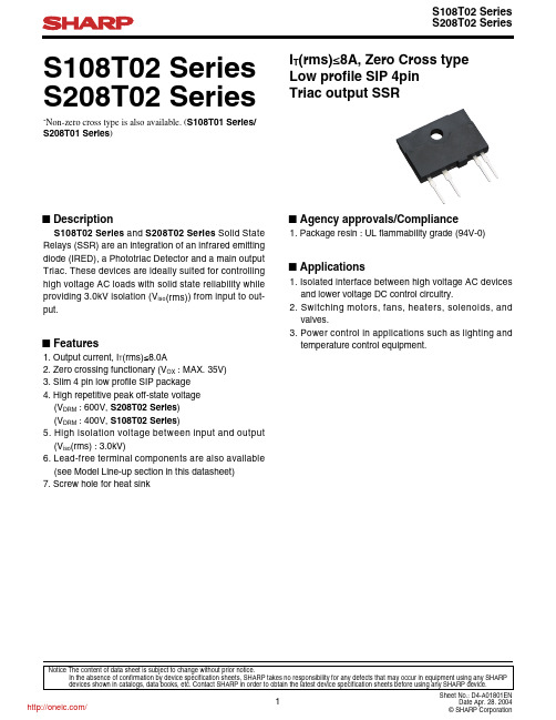
S108T02 Series S208T02 Series■ FeaturesI T (rms)≤8A, Zero Cross type Low profile SIP 4pin Triac output SSR1. Output current, I T (rms)≤8.0A2. Zero crossing functionary (V OX : MAX. 35V)3. Slim 4 pin low profile SIP package4. High repetitive peak off-state voltage (V DRM : 600V, S208T02 Series ) (V DRM : 400V, S108T02 Series )5. High isolation voltage between input and output (V iso (rms) : 3.0kV)6. Lead-free terminal components are also available (see Model Line-up section in this datasheet)7. Screw hole for heat sink■ DescriptionS108T02 Series and S208T02 Series Solid State Relays (SSR) are an integration of an infrared emitting diode (IRED), a Phototriac Detector and a main output Triac. These devices are ideally suited for controlling high voltage AC loads with solid state reliability while providing 3.0kV isolation (V iso (rms)) from input to out-put.Notice The content of data sheet is subject to change without prior notice.In the absence of confirmation by device specification sheets, SHARP takes no responsibility for any defects that may occur in equipment using any SHARP ■ Agency approvals/Compliance1. Isolated interface between high voltage AC devices and lower voltage DC control circuitry.2. Switching motors, fans, heaters, solenoids, and valves.3. Power control in applications such as lighting and temperature control equipment.■ Applications1. Package resin : UL flammability grade (94V-0)∗Non-zero cross type is also available. (S108T01 Series/S208T01 Series)∗ : Do not allow external connection.( ) : Typical dimensions■ Internal Connection Diagram+)−)■ Outline Dimensions(Unit : mm)Date code (2 digit)Rank markThere is no rank mark indicator and currently there are no rank offered for this device.A.D.199019911992199319941995199619971998199920002001MarkABCDEFHJKLMN Mark P R S T U V W X A B C Mark 123456789O N DMonth January February March April May June July August September October November December A.D 20022003200420052006200720082009201020112012······2nd digitMonth of production 1st digitYear of productionCountry of originJapanrepeats in a 20 year cycle■ Electro-optical CharacteristicsParameter Symbol Unit InputOutput (T a =25˚C)Forward voltageReverse currentRepetitive peak OFF-state currentON-state voltageHolding currentCritical rate of rise of OFF-state voltageCritical rate of rise of OFF-state voltage at commutaion Minimum trigger currentZero cross voltageIsolation resistanceTurn-on time Turn-off timeThermal resistanceV F I R I DRM V T (rms)I H dV/dt (dV/dt)c I FT V OX R ISO t ont off R th (j-c)R th (j-a)I F =20mA V R =3V V D =V DRM I T (rms)=2A, Resistance load, I F =20mA −V D =2/3•V DRM T j =125˚C , V D =2/3•V DRM , dI T /dt =−4.0A/msV D =6V, R L =30ΩI F =8mA DC500V, 40 to 60%RH V D (rms)=100V, AC50Hz, I F =20mAI T (rms)=2A, Resistance load V D (rms)=200V, AC50Hz, I F =20mA I T (rms)=2A, Resistance load V D (rms)=100V, AC50Hz, I F =20mAI T (rms)=2A, Resistance loadV D (rms)=200V, AC50Hz, I F =20mAI T (rms)=2A, Resistance loadBetween junction and case Between junction and ambience Conditions MIN.TYP.MAX.Transfer charac-teristics S108T02S208T02S108T02S208T02−−−−−305−−1010−−−−−−1.2−−−−−−−−−−−−−4.5401.41001001.550−−835−10101010−−V µA µA V mA V/µs V/µs mA V Ωmsms˚C /W ■ Absolute Maximum RatingsParameter Symbol Rating UnitInputOutput(T a =25˚C)Forward current Reverse voltage RMS ON-state current Peak one cycle surge current Repetitive peak OFF-state voltage Non-Repetitive peak OFF-state voltage Critical rate of rise of ON-state current Operating frequency Isolation voltage Operating temperature Storage temperature Soldering temperature *2*1I FV R I T (rms)I surge V DRMV DSMdI T /dt fV iso (rms)T opr T stg T solmA V A A VVA/µs Hz kV ˚C ˚C ˚C*3*3*45068804006004006005045 to 653.0−25 to +100−30 to +125260*1 40 to 60%RH, AC for 1minute, f =60Hz *2 For 10s*3 Refer to Fig.1, Fig.2*4 f =60Hz sine wave, T j =25˚C startS108T02S208T02S108T02S208T02Soldering areaShipping PackageModel No.Sleeve 25pcs/sleeve S108T02F S208T02FI FT [mA](V D =6V, R L =30Ω)MAX.8400MAX.8600V DRM [V]Please contact a local SHARP sales representative to see the actual status of the production.■ Model Line-up (1) (Lead-free terminal components)■ Model Line-up (2) (Lead solder plating components)Shipping PackageModel No.Sleeve 25pcs/sleeve S108T02S208T02I FT [mA](V D =6V, R L =30Ω)MAX.8400MAX.8600V DRM [V]F o r w a r d c u r r e n t I F (m A )Ambient temperature T a (˚C)060−2502550751001255040302010Fig.1 Forward Current vs. AmbientTemperatureFig.2 RMS ON-state Current vs.Ambient TemperatureF o r w a r d c u r r e n t I F (m A )Forward voltage V F (mA)1010.1100Fig.4 Forward Current vs. Forward VoltageFig.3 RMS ON-state Current vs.Case TemperatureR M S O N -s t a t e c u r r e n t I T (r m s )(A )Case temperature T C (°C)010−25255075100125987654321R M S O N -s t a t e c u r r e n t I T (r m s )(A )Ambient temperature T a (˚C)0987654321−25100755025125(1)(2)(3)(4)(5)(1)With infinite heat sink(2)With heat sink (200×200×2mm Al plate)(3)With heat sink (100×100×2mm Al plate)(4)With heat sink (50×50×2mm Al plate)(5)Without heat sink(N ote)In natural cooling condition, please locate Al platevertically, spread the thermal conductive silicone grease on the touch surface of the device and tighten up the device in the center of Al plate at the torque of 0.4N•m.Fig.8-b Repetitive Peak OFF-state Current vs.Ambient Temperature (S208T02)Fig.8-a Repetitive Peak OFF-state Current vs.Ambient Temperature (S108T02)R e p e t i t i v e p e a k O F F -s t a t e c u r r e n t I D R M (A )Ambient temperature T a (˚C)10−910−310−410−510−610−710−8R e p e t i t i v e p e a k O F F -s t a t e c u r r e n t I D R M (A )Ambient temperature T a (˚C)10−910−310−410−510−610−710−8Remarks : Please be aware that all data in the graph are just for reference.Fig.5 Surge Current vs. Power-on CycleFig.6 Minimum Trigger Current vs.Ambient TemperatureFig.7 Maximum ON-state Power Dissipationvs. RMS ON-state CurrentM i n i m u m t r i g g e r c u r r e n t I F T (m A )Ambient temperature T a (°C)0108642S u r g e c u r r e n t I s u r g e (A )Power-on cycle (Times)10080604020120M a x i m u m O N -s t a t e p o w e r d i s s i p a t i o n (W )RMS ON-state current I T (rms)(A)010864297531■ Design ConsiderationsIn order for the SSR to turn off, the triggering current (l F ) must be 0.1mA or less.When the input current (I F ) is below 0.1mA, the output Triac will be in the open circuit mode. However, if the voltage across the Triac, V D , increases faster than rated dV/dt, the Triac may turn on. To avoid this situation, please incorporate a snubber circuit. Due to the many different types of load that can be driven, we can merely recommend some circuit vales to start with : Cs=0.022µF and Rs=47Ω. The operation of the SSR and snubber circuit should be tested and if unintentional switching occurs, please adjust the snubber circuit component values accordingly.When making the transition from On to Off state, a snubber circuit should be used ensure that sudden drops in current are not accompanied by large instantaneous changes in voltage across the Triac.This fast change in voltage is brought about by the phase difference between current and voltage. Primarily, this is experienced in driving loads which are inductive such as motors and solenoids. Following the procedure outlined above should provide sufficient results. For over voltage protection, a Varistor may be used.Any snubber or Varistor used for the above mentioned scenarios should be located as close to the main out-put triac as possible.Particular attention needs to be paid when utilizing SSRs that incorporate zero crossing circuitry.If the phase difference between the voltage and the current at the output pins is large enough, zero crossing type SSRs cannot be used. The result, if zero crossing SSRs are used under this condition, is that the SSR may not turn on and off irregardless of the input current. In this case, only a non zero cross type SSR should be used in combination with the above mentioned snubber circuit selection process.The load current should be within the bounds of derating curve. (Refer to Fig.2) Also, please use the optional heat sink when necessary.In case the optional heat sink is used and the isolation voltage between the device and the optional heat sink is needed, please locate the insulation sheet between the device and the heat sink.When the optional heat sink is equipped, please set up the M3 screw-fastening torque at 0.3 to 0.5N•m.In order to dissipate the heat generated from the inside of device effectively, please follow the below sugges-tions.● Design guide● Recommended Operating ConditionsParameterS108T02S208T02Symbol Unit InputOutputInput signal current at ON state Input signal current at OFF state Load supply voltage Load supply currentFrequencyOperating temperatureI F (ON)I F (OFF)V OUT (rms)I OUT (rms)f T oprmA mA V mA Hz ˚C−−−Locate snubber circuit between output terminals(Cs =0.022µF, Rs =47Ω)−−Conditions(∗) See Fig.2 about derating curve (I T (rms) vs. ambient temperature).16080800.147−20240.1120240I T (rms)×80%(∗)6380MIN.MAX.✩ For additional design assistance, please review our corresponding Optoelectronic Application Notes.● Standard CircuitV +V S108T02● DegradationIn general, the emission of the IRED used in SSR will degrade over time.In the case where long term operation and / or constant extreme temperature fluctuations will be applied to the devices, please allow for a worst case scenario of 50% degradation over 5years.Therefore in order to maintain proper operation, a design implementing these SSRs should provide at least twice the minimum required triggering current from initial operation.(a) Make sure there are no warps or bumps on the heat sink, insulation sheet and device surface.(b) Make sure there are no metal dusts or burrs attached onto the heat sink, insulation sheet and device sur-face.(c) Make sure silicone grease is evenly spread out on the heat sink, insulation sheet and device surface.Silicone grease to be used is as follows;1) There is no aged deterioration within the operating temperature ranges.2) Base oil of grease is hardly separated and is hardly permeated in the device.3) Even if base oil is separated and permeated in the device, it should not degrade the function of a device. Recommended grease : G-746 (Shin-Etsu Chemical Co., Ltd.): G-747 (Shin-Etsu Chemical Co., Ltd.): SC102 (Dow Corning Toray Silicone Co., Ltd.) In case the optional heat sink is screwed up, please solder after screwed.In case of the lead frame bending, please keep the following minimum distance and avoid any mechanical stress between the base of terminals and the molding resin.Some of AC electromagnetic counters or solenoids have built-in rectifier such as the diode.In this case, please use the device carefully since the load current waveform becomes similar with rectangu-lar waveform and this results may not make a device turn off.■ Manufacturing Guidelines● Soldering MethodFlow Soldering (No solder bathing)Flow soldering should be completed below 260˚C and within 10s.Preheating is within the bounds of 100 to 150˚C and 30 to 80s.Please solder within one time.Other noticesPlease test the soldering method in actual condition and make sure the soldering works fine, since the impact on the junction between the device and PCB varies depending on the tooling and soldering conditions.分销商库存信息:SHARP-MICROELECTRONICSS108T02S108T02F S208T02。
华为H3C S1208以太网交换机 说明书

H3C S1208以太网交换机用户手册杭州华为三康技术有限公司资料版本:T1-UM-20061116-1.03声明Copyright ©2005-2006 杭州华为三康技术有限公司版权所有,保留一切权利。
非经本公司书面许可,任何单位和个人不得擅自摘抄、复制本书内容的部分或全部,并不得以任何形式传播。
H3C、Aolynk、、IRF、H3Care、、Neocean、、TOP G、SecEngine、SecPath、COMWARE、VVG、V2G、V n G、PSPT、NetPilot、XGbus均为杭州华为三康技术有限公司的商标。
对于本手册中出现的其它公司的商标、产品标识及商品名称,由各自权利人拥有。
除非另有约定,本手册仅作为使用指导,本手册中的所有陈述、信息和建议不构成任何明示或暗示的担保。
如需要获取最新手册,请登录。
技术支持用户支持邮箱:soho@技术支持热线电话:400-810-0504网址:前言本书约定1. 各类标志本书还采用各种醒目标志来表示在操作过程中应该特别注意的地方,这些标志的意义如下:小心、注意:提醒操作中应注意的事项,不当的操作可能会导致数据丢失或者交换机损坏。
说明、提示、窍门、思考:对操作内容的描述进行必要的补充和说明。
环境保护本产品符合关于环境保护方面的设计要求,产品的存放、使用和弃置应遵照相关国家法律、法规要求进行。
目录第1章产品介绍...............................................................................1-11.1 产品简介.............................................................................1-11.2 产品特性.............................................................................1-11.3 硬件介绍.............................................................................1-21.3.1 产品外观..................................................................1-21.3.2 指示灯说明...............................................................1-3第2章安装......................................................................................2-12.1 安装前的准备......................................................................2-12.1.1 安全注意事项...........................................................2-12.1.2 安装场所要求...........................................................2-22.1.3 电磁环境要求...........................................................2-22.2 安装....................................................................................2-32.2.1 脚垫安装..................................................................2-32.2.2 电源线连接...............................................................2-32.2.3 安装完成后检查.......................................................2-3第1章产品介绍1.1 产品简介H3C S1208以太网交换机(以下简称S1208)是一款无管理的二层线速千兆以太网交换产品。
Lenovo CE0128T交换机说明书

Lenovo CE0128T Switch (Gigabit Ethernet)Product Guide (withdrawn product)The Lenovo CE0128T Switch is a 1 Gb Ethernet (GbE) switch that delivers a compact, high-density, cost-effective GbE solution for small network environments where space and power are at a premium. Featuring a small, 1U footprint, this switch is designed for access-layer deployments in branches, retail and workgroup environments, and network access in larger networks.The CE0128T Switch offers 24x 10/100/1000BASE-T ports for server, storage, and network connectivity and 4x 1 GbE SFP uplink ports for connections to higher-layer devices.The CE0128T Switch supports a wide range of L2 and L3 features that provide performance, availability, security, and manageability for campus networks.The Lenovo CE0128T Switch is shown in the following figure.Figure 1. Lenovo CE0128T SwitchDid you know?The CE0128T Switch is designed to deliver non-blocking, line-rate throughput.The CE0128T Switch supports the GARP VLAN Registration Protocol (GVRP) protocol for simplifying and automating VLAN configuration.The CE0128T Switch supports stacking, enabling up to eight interconnected CE0128T Switch devices to be managed as a single logical device.The CE1028T Switch supports Zero Touch Provisioning, which enables a switch to automatically provision itself using the resources available on the network, without manual intervention.Click here to check for updatesFigure 2. Front panel of the CE0128T SwitchThe front panel of the CE0128T Switch contains the following components: 24x 1000BASE-T Ethernet ports for 10/100/1000 Mbps connections.4x SFP ports for 1 GbE transceivers: 1000BASE-T, SX, or LX.1x RJ-45 RS-232 console port for configuring the switch.LEDs that display the status of the switch and the network.Reset button.Figure 3. Rear panel of the CE0128T SwitchThe rear panel of the CE0128T Switch contains the following components: AC / HVDC power connector (IEC 320-C14).Ventilation holes.Grounding pole.Storage connectivityThe following table lists the storage systems that Lenovo offers in China that can be used with the CE0128T Switch for external 1 GbE NAS or 1 Gb iSCSI SAN storage connectivity.Table 7. External storage systemsDescription Part numberLenovo ThinkSystem DS Series Storage (1 Gb iSCSI connectivity)Lenovo ThinkSystem DS2200 LFF FC/iSCSI Dual Controller Unit (Simplified Chinese documentation)4599A3C Lenovo ThinkSystem DS2200 SFF FC/iSCSI Dual Controller Unit (Simplified Chinese documentation)4599A1C Lenovo ThinkSystem DS4200 LFF FC/iSCSI Dual Controller Unit (Simplified Chinese documentation)4617A3C Lenovo ThinkSystem DS4200 SFF FC/iSCSI Dual Controller Unit (Simplified Chinese documentation)4617A1C Lenovo ThinkSystem DS6200 SFF FC/iSCSI Dual Controller Unit (Simplified Chinese documentation)4619A1C Lenovo Storage V Series (1 Gb iSCSI connectivity)Lenovo Storage V3700 V2 LFF Control Enclosure6535C1D Lenovo Storage V3700 V2 LFF Control Enclosure (TopSeller)6535EC1 Lenovo Storage V3700 V2 SFF Control Enclosure6535C2D Lenovo Storage V3700 V2 SFF Control Enclosure (TopSeller)6535EC2 Lenovo Storage V3700 V2 XP LFF Control Enclosure6535C3D Lenovo Storage V3700 V2 XP LFF Control Enclosure (TopSeller)6535EC3 Lenovo Storage V3700 V2 XP SFF Control Enclosure6535C4D Lenovo Storage V3700 V2 XP SFF Control Enclosure (TopSeller)6535EC4 Lenovo Storage V5030 LFF Control Enclosure 3Yr S&S6536C12 Lenovo Storage V5030 LFF Control Enclosure 5Yr S&S6536C32 Lenovo Storage V5030 SFF Control Enclosure 3Yr S&S6536C22 Lenovo Storage V5030 SFF Control Enclosure 5Yr S&S6536C42 Lenovo Storage V5030F SFF Control Enclosure 3Yr S&S6536B1F Lenovo Storage V5030F SFF Control Enclosure 5Yr S&S6536B2F Lenovo Storage V7000 SFF Control Enclosure 3Yr S&S PRC6538R11^ Lenovo Storage V7000 SFF Control Enclosure 5Yr S&S PRC6538R21^ Lenovo Storage V7000F SFF Control Enclosure 3Yr S&S PRC6538R1G^ Lenovo Storage V7000F SFF Control Enclosure 5Yr S&S PRC6538R2G^ IBM Storwize for Lenovo (1 Gb iSCSI connectivity)IBM Storwize V3500 3.5-inch Dual Control Storage Controller Unit6096CU2 IBM Storwize V3500 2.5-inch Dual Control Storage Controller Unit6096CU3 IBM Storwize V7000 SFF Control Enclosure, 3YR SWMA6195C32 IBM Storwize V7000 SFF Control Enclosure, 5YR SWMA6195C52 Lenovo Storage DX8200N Series (1 GbE NAS, 1 Gb iSCSI connectivity)Lenovo Storage DX8200N with 1x N2226 HBA (Requires a supported external drive enclosure)5128C1C Lenovo Storage DX8200N with 2x N2226 HBAs (Requires a supported external drive enclosure)5128C2C Lenovo Storage DX8200C Series (1 GbE S3 cloud storage)Lenovo Storage DX8200C 56TB (14x 4TB HDDs) with Cloudian HyperStore - 3yr HW/SW S&S5120D1C Lenovo Storage DX8200C 84TB (14x 6TB HDDs) with Cloudian HyperStore - 3yr HW/SW S&S5120D2CPower distribution unitsThe following table lists the power distribution units (PDUs) that are offered by Lenovo that can be used with the CE0128T Switch in IT solutions.Table 9. Power distribution unitsDescription Part number0U Basic PDUs0U 36 C13/6 C19 32A/200-240V 1 Phase PDU with IEC60309 332P6 line cord00YJ777 0U 21 C13/12 C19 32A/200-240V/346-415V 3 Phase PDU with IEC60309 532P6 line cord00YJ778 0U 21 C13/12 C19 48A/200-240V 3 Phase PDU with IEC60309 460P9 line cord00YJ779 Switched and Monitored PDUs0U 20 C13/4 C19 Switched and Monitored 32A/200-240V/1Ph PDU w/ IEC60309 332P6 line cord00YJ780 0U 18 C13/6 C19 Switched / Monitored 32A/200-240V/346-415V/3Ph PDU w/ IEC60309 532P6 cord00YJ782 0U 12 C13/12 C19 Switched and Monitored 48A/200-240V/3Ph PDU w/ IEC60309 460P9 line cord00YJ783 1U 9 C19/3 C13 Switched and Monitored DPI PDU (without line cord)46M4002 1U 9 C19/3 C13 Switched and Monitored 60A 3Ph PDU with IEC 309 3P+Gnd cord46M4003 1U 12 C13 Switched and Monitored DPI PDU (without line cord)46M4004 1U 12 C13 Switched and Monitored 60A 3 Phase PDU with IEC 309 3P+Gnd line cord46M4005 Ultra Density Enterprise PDUs (9x IEC 320 C13 + 3x IEC 320 C19 outlets)Ultra Density Enterprise C19/C13 PDU Module (without line cord)71762NX Ultra Density Enterprise C19/C13 PDU 60A/208V/3ph with IEC 309 3P+Gnd line cord71763NU C13 Enterprise PDUs (12x IEC 320 C13 outlets)DPI C13 Enterprise PDU+ (without line cord)39M2816 DPI Single Phase C13 Enterprise PDU (without line cord)39Y8941 C19 Enterprise PDUs (6x IEC 320 C19 outlets)DPI Single Phase C19 Enterprise PDU (without line cord)39Y8948 DPI 60A 3 Phase C19 Enterprise PDU with IEC 309 3P+G (208 V) fixed line cord39Y8923 Front-end PDUs (3x IEC 320 C19 outlets)DPI 32amp/250V Front-end PDU with IEC 309 2P+Gnd line cord39Y8934 DPI 60amp/250V Front-end PDU with IEC 309 2P+Gnd line cord39Y8940 DPI 63amp/250V Front-end PDU with IEC 309 2P+Gnd line cord39Y8935 Universal PDUs (7x IEC 320 C13 outlets)DPI Universal 7 C13 PDU (with 2 m IEC 320-C19 to C20 rack power cord)00YE443 Line cords for PDUs that ship without a line cordDPI 32a Line Cord (IEC 309 P+N+G)40K9612 DPI 32a Line Cord (IEC 309 3P+N+G)40K9611 DPI 60a Cord (IEC 309 2P+G)40K9615 DPI 63a Cord (IEC 309 P+N+G)40K9613For more information, see the list of Product Guides in the PDU category:https:///servers/options/pdu#rt=product-guideUninterruptible power supply unitsUninterruptible power supply unitsThe following table lists the uninterruptible power supply (UPS) units that are offered by Lenovo that can be used with the CE0128T Switch in IT solutions.Table 10. Uninterruptible power supply unitsDescription Part numberRT1.5kVA 2U Rack or Tower UPS (200-240VAC) (8x IEC 320 C13 10A outlets)55941KX RT2.2kVA 2U Rack or Tower UPS (200-240VAC) (8x IEC 320 C13 10A, 1x IEC 320 C19 16A outlets)55942KX RT3kVA 2U Rack or Tower UPS (200-240VAC) (8x IEC 320 C13 10A, 1x IEC 320 C19 16A outlets)55943KX RT5kVA 3U Rack or Tower UPS (200-240VAC) (8x IEC 320 C13 10A, 2x IEC 320 C19 16A outlets)55945KX RT6kVA 3U Rack or Tower UPS (200-240VAC) (8x IEC 320 C13 10A, 2x IEC 320 C19 16A outlets)55946KX RT8kVA 6U Rack or Tower UPS (200-240VAC) (4x IEC 320-C19 16A outlets)55948KX RT11kVA 6U Rack or Tower UPS (200-240VAC) (4x IEC 320-C19 16A outlets)55949KX RT8kVA 6U 3:1 Phase Rack or Tower UPS (380-415VAC) (4x IEC 320-C19 16A outlets)55948PX RT11kVA 6U 3:1 Phase Rack or Tower UPS (380-415VAC) (4x IEC 320-C19 16A outlets)55949PXFor more information, see the list of Product Guides in the Uninterruptible Power Supply Units category: /servers/options/ups#rt=product-guideLenovo Financial ServicesLenovo Financial Services reinforces Lenovo’s commitment to deliver pioneering products and services that are recognized for their quality, excellence, and trustworthiness. Lenovo Financial Services offers financing solutions and services that complement your technology solution anywhere in the world.We are dedicated to delivering a positive finance experience for customers like you who want to maximize your purchase power by obtaining the technology you need today, protect against technology obsolescence, and preserve your capital for other uses.We work with businesses, non-profit organizations, governments and educational institutions to finance their entire technology solution. We focus on making it easy to do business with us. Our highly experienced team of finance professionals operates in a work culture that emphasizes the importance of providing outstanding customer service. Our systems, processes and flexible policies support our goal of providing customers with a positive experience.We finance your entire solution. Unlike others, we allow you to bundle everything you need from hardware and software to service contracts, installation costs, training fees, and sales tax. If you decide weeks or months later to add to your solution, we can consolidate everything into a single invoice.Our Premier Client services provide large accounts with special handling services to ensure these complex transactions are serviced properly. As a premier client, you have a dedicated finance specialist who manages your account through its life, from first invoice through asset return or purchase. This specialist develops an in-depth understanding of your invoice and payment requirements. For you, this dedication provides a high-quality, easy, and positive financing experience.For your region specific offers please ask your Lenovo sales representative or your technology provider about the use of Lenovo Financial Services. For more information, see the following Lenovo website: Related publications and linksTrademarksLenovo and the Lenovo logo are trademarks or registered trademarks of Lenovo in the United States, other countries, or both. A current list of Lenovo trademarks is available on the Web athttps:///us/en/legal/copytrade/.The following terms are trademarks of Lenovo in the United States, other countries, or both:Lenovo®RackSwitchThinkSystem®TopSellerOther company, product, or service names may be trademarks or service marks of others.。
- 1、下载文档前请自行甄别文档内容的完整性,平台不提供额外的编辑、内容补充、找答案等附加服务。
- 2、"仅部分预览"的文档,不可在线预览部分如存在完整性等问题,可反馈申请退款(可完整预览的文档不适用该条件!)。
- 3、如文档侵犯您的权益,请联系客服反馈,我们会尽快为您处理(人工客服工作时间:9:00-18:30)。
S108T01 Series S208T01 Series■ FeaturesI T (rms)≤8A, Non-Zero Cross type Low profile SIP 4pin Triac output SSR1. Output current, I T (rms)≤8.0A2. Non-zero crossing functionary3. Slim 4 pin low profile SIP package4. High repetitive peak off-state voltage (V DRM : 600V, S208T01 Series ) (V DRM : 400V, S108T01 Series )5. High isolation voltage between input and output (V iso (rms) : 3.0kV)6. Lead-free terminal components are also available (see Model Line-up section in this datasheet)7. Screw hole for heat sink■ DescriptionS108T01 Series and S208T01 Series Solid State Relays (SSR) are an integration of an infrared emitting diode (IRED), a Phototriac Detector and a main output Triac. These devices are ideally suited for controlling high voltage AC loads with solid state reliability while providing 3.0kV isolation (V iso (rms)) from input to out-put.Notice The content of data sheet is subject to change without prior notice.In the absence of confirmation by device specification sheets, SHARP takes no responsibility for any defects that may occur in equipment using any SHARP ■ Agency approvals/Compliance1. Isolated interface between high voltage AC devices and lower voltage DC control circuitry.2. Switching motors, fans, heaters, solenoids, and valves.3. Phase or power control in applications such as light-ing and temperature control equipment.■ Applications1. Package resin : UL flammability grade (94V-0)∗Zero cross type is also available. (S108T02 Series/S208T02 Series)∗ : Do not allow external connection.( ) : Typical dimensions■Internal Connection DiagramOutput (Triac T1)Output (Triac T2)Input (+)Input (−)■ Outline Dimensions(Unit : mm)Date code (2 digit)Rank markThere is no rank mark indicator and currently there are no rank offered for this device.A.D.199019911992199319941995199619971998199920002001MarkABCDEFHJKLMN Mark P R S T U V W X A B C Mark 123456789O N DMonth January February March April May June July August September October November December A.D 20022003200420052006200720082009201020112012······2nd digitMonth of production 1st digitYear of productionCountry of originJapanrepeats in a 20 year cycle■ Electro-optical CharacteristicsParameter Symbol Unit InputOutput (T a =25˚C)Forward voltageReverse currentRepetitive peak OFF-state currentON-state voltageHolding currentCritical rate of rise of OFF-state voltageCritical rate of rise of OFF-state voltage at commutaion Minimum trigger currentIsolation resistanceTurn-on time Turn-off timeThermal resistanceI F =20mA V R =3V V D =V DRM I T (rms)=2A, Resistance load, I F =20mA −V D =2/3•V DRM T j =125˚C , V D =2/3•V DRM , dI T /dt =−4.0A/msV D =12V, R L =30ΩDC500V, 40 to 60%RH V D (rms)=100V, AC50Hz, I F =20mAI T (rms)=2A, Resistance loadV D (rms)=200V, AC50Hz, I F =20mAI T (rms)=2A, Resistance load V D (rms)=100V, AC50Hz, I F =20mAI T (rms)=2A, Resistance loadV D (rms)=200V, AC50Hz, I F =20mAI T (rms)=2A, Resistance loadBetween junction and case Between junction and ambience Conditions MIN.TYP.MAX.Transfer charac-teristicsS108T01S208T01S108T01S208T01V µA µA V mA V/µs V/µs mA Ωmsms˚C /W −−−−−305−1010−−−−−−1.2−−−−−−−−−−−−4.5401.41001001.550−−8−111010−−V F I R I DRM V T (rms)I H dV/dt(dV/dt)c I FT R ISO t ont off R th (j-c)R th (j-a)■ Absolute Maximum RatingsParameter Symbol Rating UnitInputOutput(T a =25˚C)Forward current Reverse voltage RMS ON-state current Peak one cycle surge current Repetitive peak OFF-state voltage Non-Repetitive peak OFF-state voltage Critical rate of rise of ON-state current Operating frequency Isolation voltage Operating temperature Storage temperature Soldering temperature *2*1I FV R I T (rms)I surge V DRMV DSMdI T /dt fV iso (rms)T opr T stg T solmA V A A VVA/µs Hz kV ˚C ˚C ˚C*3*3*45068804006004006005045 to 653.0−25 to +100−30 to +125260*1 40 to 60%RH, AC for 1minute, f =60Hz *2 For 10s*3 Refer to Fig.1, Fig.2*4 f =60Hz sine wave, T j =25˚C startS108T01S208T01S108T01S208T01Soldering areaShipping PackageModel No.Sleeve 25pcs/sleeve S108T01F S208T01FI FT [mA](V D =12V, R L =30Ω)MAX.8400MAX.8600V DRM [V]Please contact a local SHARP sales representative to see the actual status of the production.■ Model Line-up (1) (Lead-free terminal components)■ Model Line-up (2) (Lead solder plating components)Shipping PackageModel No.Sleeve 25pcs/sleeve S108T01S208T01I FT [mA](V D =12V, R L =30Ω)MAX.8400MAX.8600V DRM [V]F o r w a r d c u r r e n t I F (m A )Ambient temperature T a (˚C)060−2502550751001255040302010Fig.1 Forward Current vs. AmbientTemperatureFig.2 RMS ON-state Current vs.Ambient TemperatureR M S O N -s t a t e c u r r e n t I T (r m s )(A )Ambient temperature T a (˚C)0987654321−25100755025125(1)(2)(3)(4)(5)(1)With infinite heat sink(2)With heat sink (200×200×2mm Al plate)(3)With heat sink (100×100×2mm Al plate)(4)With heat sink (50×50×2mm Al plate)(5)Without heat sink(N ote)In natural cooling condition, please locate Al platevertically, spread the thermal conductive silicone grease on the touch surface of the device and tighten up the device in the center of Al plate at the torque of 0.4N•m.F o r w a r d c u r r e n t I F (m A )Forward voltage V F (mA)1010.1100Fig.4 Forward Current vs. Forward VoltageFig.3 RMS ON-state Current vs.Case TemperatureR M S O N -s t a t e c u r r e n t I T (r m s )(A )Case temperature T C (°C) 010−25255075100125987654321Fig.8-b Repetitive Peak OFF-state Current vs.Ambient Temperature (S208T01)Fig.8-a Repetitive Peak OFF-state Current vs.Ambient Temperature (S108T01)R e p e t i t i v e p e a k O F F -s t a t e c u r r e n t I D R M (A )Ambient temperature T a (˚C)10−910−310−410−510−610−710−8R e p e t i t i v e p e a k O F F -s t a t e c u r r e n t I D R M (A )Ambient temperature T a (˚C)10−910−310−410−510−610−710−8Remarks : Please be aware that all data in the graph are just for reference.Fig.5 Surge Current vs. Power-on CycleFig.6 Minimum Trigger Current vs.Ambient TemperatureFig.7 Maximum ON-state Power Dissipationvs. RMS ON-state CurrentM i n i m u m t r i g g e r c u r r e n t I F T (m A )Ambient temperature T a (˚C)0108642S u r g e c u r r e n t I s u r g e (A )Power-on cycle (Times)10080604020120M a x i m u m O N -s t a t e p o w e r d i s s i p a t i o n (W )RMS ON-state current I T (rms)(A)010864297531■ Design ConsiderationsIn order for the SSR to turn off, the triggering current (l F ) must be 0.1mA or less.In phase control applications or where the SSR is being by a pulse signal, please ensure that the pulse width is a minimum of 1ms.When the input current (I F ) is below 0.1mA, the output Triac will be in the open circuit mode. However, if the voltage across the Triac, V D , increases faster than rated dV/dt, the Triac may turn on. To avoid this situation, please incorporate a snubber circuit. Due to the many different types of load that can be driven, we can merely recommend some circuit vales to start with : Cs=0.022µF and Rs=47Ω. The operation of the SSR and snubber circuit should be tested and if unintentional switching occurs, please adjust the snubber circuit component values accordingly.When making the transition from On to Off state, a snubber circuit should be used ensure that sudden drops in current are not accompanied by large instantaneous changes in voltage across the Triac.This fast change in voltage is brought about by the phase difference between current and voltage. Primarily, this is experienced in driving loads which are inductive such as motors and solenoids. Following the procedure outlined above should provide sufficient results.Any snubber or Varistor used for the above mentioned scenarios should be located as close to the main out-put triac as possible.The load current should be within the bounds of derating curve. (Refer to Fig.2) Also, please use the optional heat sink when necessary.In case the optional heat sink is used and the isolation voltage between the device and the optional heat sink is needed, please locate the insulation sheet between the device and the heat sink.When the optional heat sink is equipped, please set up the M3 screw-fastening torque at 0.3 to 0.5N•m.In order to dissipate the heat generated from the inside of device effectively, please follow the below sugges-tions.(a) Make sure there are no warps or bumps on the heat sink, insulation sheet and device surface.(b) Make sure there are no metal dusts or burrs attached onto the heat sink, insulation sheet and device sur-face.(c) Make sure silicone grease is evenly spread out on the heat sink, insulation sheet and device surface.● Design guide● Recommended Operating ConditionsParameterS108T01S208T01Symbol Unit InputOutputInput signal current at ON state Input signal current at OFF state Load supply voltage Load supply currentFrequencyOperating temperatureI F (ON)I F (OFF)V OUT (rms)I OUT (rms)f T oprmA mA V mA Hz ˚C−−−Locate snubber circuit between output terminals(Cs =0.022µF, Rs =47Ω)−−Conditions(∗) See Fig.2 about derating curve (I T (rms) vs. ambient temperature).16080800.147−20240.1120240I T (rms)×80%(∗)6380MIN.MAX.✩ For additional design assistance, please review our corresponding Optoelectronic Application Notes.● Standard CircuitV 1+V CCS108T01● DegradationIn general, the emission of the IRED used in SSR will degrade over time.In the case where long term operation and / or constant extreme temperature fluctuations will be applied to the devices, please allow for a worst case scenario of 50% degradation over 5years.Therefore in order to maintain proper operation, a design implementing these SSRs should provide at least twice the minimum required triggering current from initial operation.Silicone grease to be used is as follows;1) There is no aged deterioration within the operating temperature ranges.2) Base oil of grease is hardly separated and is hardly permeated in the device.3) Even if base oil is separated and permeated in the device, it should not degrade the function of a device. Recommended grease : G-746 (Shin-Etsu Chemical Co., Ltd.): G-747 (Shin-Etsu Chemical Co., Ltd.): SC102 (Dow Corning Toray Silicone Co., Ltd.) In case the optional heat sink is screwed up, please solder after screwed.In case of the lead frame bending, please keep the following minimum distance and avoid any mechanical stress between the base of terminals and the molding resin.Some of AC electromagnetic counters or solenoids have built-in rectifier such as the diode.In this case, please use the device carefully since the load current waveform becomes similar with rectangu-lar waveform and this results may not make a device turn off.■ Manufacturing Guidelines● Soldering MethodFlow Soldering (No solder bathing)Flow soldering should be completed below 260˚C and within 10s.Preheating is within the bounds of 100 to 150˚C and 30 to 80s.Please solder within one time.Other noticesPlease test the soldering method in actual condition and make sure the soldering works fine, since the impact on the junction between the device and PCB varies depending on the tooling and soldering conditions.分销商库存信息:SHARP-MICROELECTRONICSS108T01S108T01F S208T01。