3362M中文资料
新型窄带调频接收机集成电路MC3362,MC3363,MC3364,MC3367的应用
新型窄带调频接收机集成电路MC3362,MC3363,MC3364,MC3367的应用单片接收机电路MC3362系列的出现,大大地推动了移动通信电台的革新。
这些集成电路芯片的共同特点是:功能强,单片化,电压低,低功耗,灵敏度高。
新型的低功耗窄带FM单片接收机电路MC3362,已经包含了除高放外的前端电路,而且还增加了载波检测电路和用于FSK检测的比较器,它适用于窄带话音与数据链路的通信。
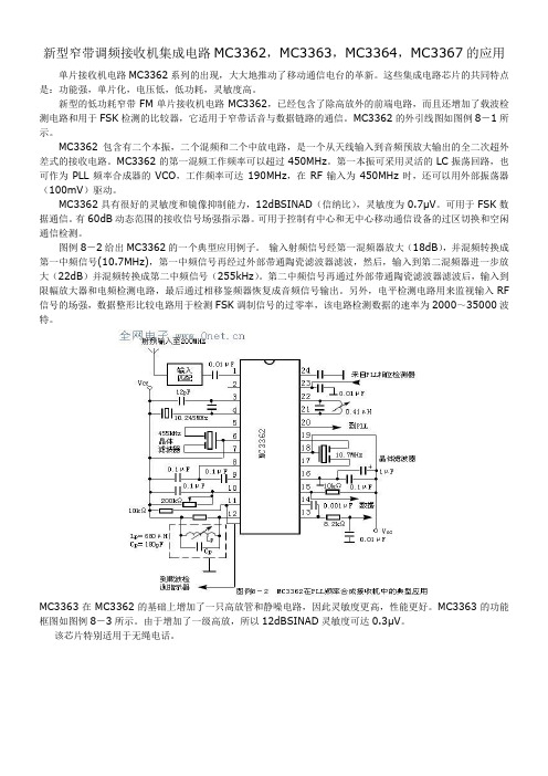
MC3362的外引线图如图例8-1所示。
MC3362包含有二个本振,二个混频和二个中放电路,是一个从天线输入到音频预放大输出的全二次超外差式的接收电路。
MC3362的第一混频工作频率可以超过450MHz。
第一本振可采用灵活的LC振荡回路,也可作为PLL频率合成器的VCO,工作频率可达190MHz,在RF输入为450MHz时,还可以用外部振荡器(100mV)驱动。
MC3362具有很好的灵敏度和镜像抑制能力,12dBSINAD(信纳比),灵敏度为0.7μV。
可用于FSK数据通信。
有60dB动态范围的接收信号场强指示器。
可用于控制有中心和无中心移动通信设备的过区切换和空闲通信检测。
图例8-2给出MC3362的一个典型应用例子。
输入射频信号经第一混频器放大(18dB),并混频转换成第一中频信号(10.7MHz),第一中频信号再经过外部带通陶瓷滤波器滤波,然后,输入到第二混频器进一步放大(22dB)并混频转换成第二中频信号(255kHz)。
第二中频信号再通过外部带通陶瓷滤波器滤波后,输入到限幅放大器和电频检测电路,最后通过相移鉴频器恢复成音频信号输出。
另外,电平检测电路用来监视输入RF 信号的场强,数据整形比较电路用于检测FSK调制信号的过零率,该电路检测数据的速率为2000~35000波特。
MC3363在MC3362的基础上增加了一只高放管和静噪电路,因此灵敏度更高,性能更好。
MC3363的功能框图如图例8-3所示。
由于增加了一级高放,所以12dBSINAD灵敏度可达0.3μV。
电位器3362

*RoHS Directive 2002/95/EC Jan 27 2003 including Annex.†“Fluorinert” is a registered trademark of 3M Co.Specifications are subject to change without notice.Customers should verify actual device performance in their specific applications.Electrical Characteristics Standard Resistance Range..................................10 to 2 megohms(see standard resistance table)Resistance Tolerance............±10 % std.(tighter tolerance available)Absolute Minimum Resistance......................................1 % or 2 ohms(whichever is greater)Contact Resistance Variation.............................1 % or 3 ohms max.(whichever is greater)AdjustabilityVoltage....................................±0.05 %Resistance..............................±0.15 %Resolution.....................................Infinite Insulation Resistance................500 vdc.1,000 megohms min.Dielectric StrengthSea Level .................................900 vac 80,000 Feet..............................350 vac Adjustment Angle..................240 °nom.Environmental Characteristics Power Rating (300 volts max.)70 °C......................................0.50 watt 125 °C.........................................0 watt Temperature Range.................................-55 °C to +125 °C Temperature Coefficient........................................±100 ppm/°C Seal Test........................85 °C Fluorinert †-STD-202 Method 10396 hours(2 % ∆TR; 10 Megohms IR)Vibration.........30 G (1 % ∆TR; 1 % ∆VR)Shock...........100 G (1 % ∆TR; 1 % ∆VR)Load Life ..1,000 hours 0.5 watt @ 70 °C(3 % ∆TR; 3 % or 3 ohms,whichever is greater, CRV)Rotational Life........................200 cycles(4 % ∆TR; 3 % or 3 ohms,whichever is greater, CRV)Physical CharacteristicsMechanical Angle..................270 °nom.Torque .............................3.0 oz-in. max.Stop Strength..................7.0 oz -in. min.Terminals........................Solderable pins Weight ........................................0.02 oz.Marking .......................Resistance code,terminal numbers, manufacturer’smodel number, styleand date codeWiper................50 % (Actual TR) ±10 %Flammability ..........................U.L. 94V-0Standard Packaging.....50 pcs. per tube Adjustment Tool..............................H-902.293362H3362M3362ZDIA.3362CLOCKWISEDIMENSIONS ARE:MM (INCHES)TOLERANCES: ±0.25 (.010) EXCEPT WHERE NOTED*Ro H S C O M P L I A N T V E R S I O N S A V A I L A B L ESpecifications are subject to change without notice.Customers should verify actual device performance in their specific applications.Resistance Resistance (Ohms)Code 1010020200505001001012002015005011,0001022,0002025,00050210,00010320,00020325,00025350,000503100,000104200,000204250,000254500,0005041,000,0001052,000,000205Standard Resistance TablePopular distribution resistance values listed in boldface. Special resistances available.REV. 04/06How to Order3362 P - 1 - 502 T __ LFModel StyleStandard or Modified Product Indicator-1 = Standard Product Resistance Code Optional Suffix LetterT =Knob*Packaging DesignatorBlank =Tube (Standard)R =Tape and Reel(M, U and P Pin Styles Only)A =Ammo Pack(M, U and P Pin Styles Only)TerminationsLF =100 % Tin-plated (RoHS compliant)Blank =90 % Tin / 10 % Lead-plated(Standard)*Knob option is available only in standard Tube packaging for terminal styles H, P , R and U.Consult factory for other available options.Packaging Specifications ALL PINS IN-LINE ON CENTERDIMENSIONS:1000/REEL/BOX2.54(.100) MM(INCHES) TOP ADJUST3362U-1, 3362P-1SIDE VIEW 3362U-1SIDE VIEW 3362P-1ALL PINS IN-LINE ON CENTERDIMENSIONS:750/REEL 1000/BOX2.54(.100) MM(INCHES) Meets EIA Specification 468.Top adjust models 3362H, P , R and U are available with a knob for finger adjustment.Add suffix letter “T” to order code.DIMENSIONS: MM/(INCHES)TOLERANCES: ±.25/(±.010) EXCEPT WHERE NOTEDProduct Dimensions。
3362P精密可调电位器
产品名称Product Name 精密电位器
型
号Model No
JML3362系列
≤1%R or 2Ω
5.接触电阻变化Contact Resistance Variation 3%R or 3Ω 6.绝缘电阻Insulation resistance 7.耐电压Withstand Voltage 8.有效电行程Effective Electrical Travel R1≥1GΩ 101.3 KPa 500V, 8.5Kpa315V 210º ±10º
B.环境特性Environmental Characteristics
1.额定功率(最高工作电压300V) Rated Power(max. working voltage 300V) 2.工作温度范围Temperature Range 3.温度系数TCR 4.温度变化Temperature Variation 5.碰撞Collision 6.振动Vibration 7.气候顺序Climate Category +70℃ 0.5W,+125℃ 0W -55℃~ +125℃ ±200ppm/℃ △R≤±(2%R+0.1Ω),△(Uab/Uac)≤±2% 390m/s2,4000次 , △R≤±2%R 10~2000Hz,0.75mm,6h △R≤±1%R,△(Uab/Uac)≤±2% △R≤±3%R,R1≥100MΩ
料
号Part NO
6A1001004系列
A.电位器性能Electrical characteristics
mc3362无线接收
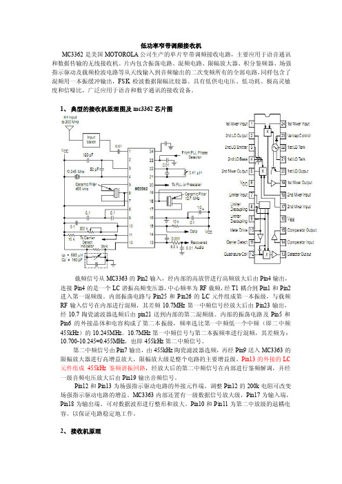
低功率窄带调频接收机MC3362是美国MOTOROLA公司生产的单片窄带调频接收电路,主要应用于语音通讯和数据传输的无线接收机。
片内包含振荡电路、混频电路、限幅放大器、积分鉴频器、场强指示驱动及载频检波电路等从天线输入到音频输出的二次变频所有的全部电路,同样包含了混频用一本振缓冲输出,FSK检波数据限幅比较器。
具有低供电电压、低功耗、极高灵敏度和信噪比,广泛应用于语音和数字通讯的接收设备。
1、典型的接收机原理图及mc3362芯片图载频信号从MC3363的Pin2输入,经内部的高放管进行高频放大后由Pin4输出,连接Pin4的是一个LC谐振高频变压器,中心频率为RF载频,经T1耦合到Pin1和Pin2进入第一混频级。
内部振荡电路与Pin25和Pin26的LC元件组成第一本振级,与载频RF输入信号在内部进行混频,其差频10.7MHz第一中频信号经放大后由Pin23输出,经10.7陶瓷滤波器选频后由pin21送到内部的第二混频级。
内部的振荡电路及Pin5和Pin6的外接晶体和电容构成了第二本振级,频率选比第一中频低一个中频(即二中频455kHz)的10.245MHz。
10.7MHz第一中频信号与第二本振频率进行混频,其差频为:10.700-10.245=0.455MHz,也即455kHz第二中频信号。
第二中频信号由Pin7输出,由455kHz陶瓷滤波器选频,再经Pin9送入MC3363的限幅放大器进行高增益放大,限幅放大级是整个电路的主要增益级。
Pin13的外接的LC 元件组成455kHz鉴频谐振回路,经放大后的第二中频信号在内部进行鉴频解调,并经一级音频电压放大后由Pin19输出音频信号。
Pin12和Pin13为场强指示驱动电路的外接元件端,调整Pin12的200k电阻可改变场强指示驱动电路的增益。
MC3363内部还置有一级数据信号放大级,Pin17为输入端,Pin18为输出端。
可对数据波形进行整形和放大。
3362LT中文资料

The A3361x and A3362x Hall-effect switches are extremelytemperature-stable and stress-resistant sensors. Superior performance over temperature is made possible through dynamic offset cancellation,which reduces the residual offset voltage normally caused by device overmolding, temperature dependencies, and thermal stress. The two devices differ only in output polarity; the A3361x output current goes low in the presence of a south pole of sufficient strength; the A3362x output current goes high.Each device includes on a single silicon chip a voltage regulator,Hall-voltage generator, small-signal amplifier, chopper stabilization,Schmitt trigger, and a constant-current open-collector output. An on-board regulator permits operation with supply voltages of 3.5 to 24volts. Noise radiation is limited by control of the output current slew rate.Three package styles provide a magnetically optimized package for most applications. Suffix ‘xLH’ is a miniature low-profile surface-mount package, ‘xLT’ is a miniature SOT-89/TO-243AA transistor package for surface-mount applications; while suffix ‘xUA’ is a three-lead ultra-mini-SIP for through-hole mounting.FEATURESI Internal Current Regulator for 2-Wire Operation I Resistant to Physical Stress I Superior Temperature Stability I Operation From Unregulated Supply I Solid-State Reliability I Small SizeAlways order by complete part number: the prefix 'A' + the basic four-digitpart number + a suffix to indicate operating temperature range (E) +a two-letter suffix to indicate package style, e.g., A3361ELH .2-WIRE, CHOPPER-STABILIZED,HALL-EFFECT SWITCHES3361 AND 3362Data Sheet 27621.503361 AND 33622-WIRE,CHOPPER-STABILIZED,HALL-EFFECT SWITCHES115 Northeast Cutoff, Box 15036Worcester, Massachusetts 01615-0036 (508) 853-50002Copyright © 2000, Allegro MicroSystems, Inc.Pinning is shown viewed from branded side.Dwg. PH-003-6S U P P L YG R O U N DN O (I N T E R N A L )C O N N E C T I O NDwg. PH-003-7A S U P P L YG R O U N DG R O U N DSuffix Code 'UA' Pinning(SIP)Suffix Code 'LT' Pinning (SOT-89/TO-243AA)3361 AND 33622-WIRE,CHOPPER-STABILIZED,HALL-EFFECT SWITCHES3A3361 MAGNETIC CHARACTERISTICS over operating supply voltage and temperature ranges.LimitsCharacteristic Symbol Test Conditions Min.Typ.Max.Units Operate Point B OP B > B OP , I GND = LOW ––125G Release Point B RP B < B RP , I GND = HIGH 40––G HysteresisB hysB OP - B RP5.0–30GA3362 MAGNETIC CHARACTERISTICS over operating supply voltage and temperature ranges.LimitsCharacteristic Symbol Test Conditions Min.Typ.Max.Units Operate Point B OP B > B OP , I GND = HIGH ––125G Release Point B RP B < B RP , I GND = LOW 40––G HysteresisB hysB OP - B RP5.0–30GELECTRICAL CHARACTERISTICS over operating temperature range.LimitsCharacteristic Symbol Test Conditions Min.Typ.Max.Units Supply Voltage V CC Operating3.51224V Output CurrentI GND(L)Output Current Low 5.0– 6.9mA I GND(H)Output Current High12–17mA Chopping Frequency f C –340–kHz Output Settling Time t sd C L = 20 pF ––50µs Output Rise Time t r C L = 20 pF – 3.5–µs Output Fall Time t f C L = 20 pF – 3.5–µs Reverse Battery CurrentI CCV RCC = -16 V ––-15mANOTE:Typical Data is at T A = +25°C and V CC = 12 V and is for design information only.3361 AND 33622-WIRE,CHOPPER-STABILIZED,HALL-EFFECT SWITCHES115 Northeast Cutoff, Box 15036Worcester, Massachusetts 01615-0036 (508) 853-50004O U T P U T C U R R E N TFLUX DENSITYDwg. GH-007-3+IOUTPUT CHARACTERISTICSA3361xA3362x+B0O U T P U T C U R R E N TFLUX DENSITYDwg. GH-007-4RP B OP B I OUT + I CC I CC +I3361 AND 33622-WIRE,CHOPPER-STABILIZED,HALL-EFFECT SWITCHES5SENSOR LOCATIONS(±0.005” [0.13 mm] die placement)Package Designator “LH”Package Designators “UA” and "UA-TL"Although sensor location is accurate to three sigma for a particular design, product improvements may result in small changes to sensor location.0.011"0.28 mm NOMDwg. MH-008-80.030"0.76 mm NOMDwg. MH-011-9APackage Designator “LT”60040020020601001400AMBIENT TEMPERATURE in °CA L L O W AB L E P AC K A G E P O W E RD I S S I P A T I O N i n M I L L I W A T T SDwg. GH-046-440801201807005003001001603361 AND 33622-WIRE,CHOPPER-STABILIZED,HALL-EFFECT SWITCHES115 Northeast Cutoff, Box 15036Worcester, Massachusetts 01615-0036 (508) 853-50006All Allegro sensors are subjected to stringent qualification requirements prior to being released to production.To become qualified, except for the destructive ESD tests, no failures are permitted.CRITERIA FOR DEVICE QUALIFICATIONQualification Test Test Method and Test Conditions Test Length SamplesComments Biased Humidity (HAST)T A = 130°C, RH = 85%50 hrs 77V CC = V OUT = 5 V High-Temperature JESD22-A108,408 hrs77V CC = 24 V,Operating Life (HTOL)T A = 150°C, T J = 165°C V OUT = 20 V Accelerated HTOLJESD22-A108,504 hrs 77V CC = 24 V,T A = 175°C, T J = 190°C V OUT = 20 VAutoclave, Unbiased JESD22-A102, Condition C,96 hrs 77T A = 121°C, 15 psig High-Temperature MIL-STD-883, Method 1008,1000 hrs 77(Bake) Storage Life T A = 170°CTemperature CycleMIL-STD-883, Method 1010,500 cycles 77-65°C to +150°C Latch-Up—Pre/Post 6Reading Electro-Thermally—Pre/Post 6Induced Gate Leakage Reading ESD,CDF-AEC-Q100-002Pre/Post x per Test to failure,Human Body Model Reading test All leads > TBDElectrical DistributionsPer Specification—303361 AND 33622-WIRE,CHOPPER-STABILIZED,HALL-EFFECT SWITCHES7FUNCTIONAL DESCRIPTION+—Dwg. AH-011-2Chopper-Stabilized Technique. The Hall element can be considered as a resistor array similar to a Wheatstone bridge. A large portion of the offset is a result of the mismatching of these resistors. These devices use a proprietary dynamic offsetcancellation technique, with an internal high-frequency clock to reduce the residual offset voltage of the Hall element that is normally caused by device overmolding, temperature dependen-cies, and thermal stress. The chopper-stabilizing technique cancels the mismatching of the resistor circuit by changing the direction of the current flowing through the Hall plate using CMOS switches and Hall voltage measurement taps, whilemaintaing the Hall-voltage signal that is induced by the external magnetic flux. The signal is then captured by a sample-and-hold circuit and further processed using low-offset bipolar circuitry. This technique produces devices that have anextremely stable quiescent Hall output voltage, are immune to thermal stress, and have precise recoverability after temperature cycling. This technique will also slightly degrade the device output repeatability. A relatively high sampling frequency is used in order that faster signals can be processed.More detailed descriptions of the circuit operation can be found in: Technical Paper STP 97-10, Monolithic Magnetic Hall Sensor Using Dynamic Quadrature Offset Cancellation and Technical Paper STP 99-1, Chopper-Stabilized Amplifiers With A Track-and-Hold Signal Demodulator .Operation. As shown in the output characteristic graphs, the output of the A3362 turns on when a magnetic field (south pole)perpendicular to the Hall sensor is increased above the operate point threshold (B OP ). After turn on, the output will source current equal to the device operating current plus a current source (I GND(H)). When the magnetic field is decreased below the release point (B RP ), the output turns off and will source current equal only to the Hall-effect sensor operating current (I GND(L)). The A3361 output is inverted and the device turns off at B OP and on at B RP . The difference in the magnetic operate and release points is the hysteresis (B hys ) of the device. The hysteresis allows clean switching of the output even in the presence of external mechanical vibration or electrical noise.Applications. It is strongly recommended that an external bypass capacitor be connected (in close proximity to the Hall sensor) between the supply and ground of the device to reduce both external noise and noise generated by the chopper-stabilization technique.Extensive applications information on magnets and Hall-effect sensors is also available in the Allegro Electronic Data Book AMS-702 or Application Note 27701 or3361 AND 33622-WIRE,CHOPPER-STABILIZED,HALL-EFFECT SWITCHES115 Northeast Cutoff, Box 15036Worcester, Massachusetts 01615-0036 (508) 853-50008PACKAGE DESIGNATOR 'LH'(fits SC-74A solder-pad layout)NOTES: 1.Tolerances on package height and width represent allowable mold offsets. Dimensions given are measured at the widest point (parting line).2.Exact body and lead configuration at vendor’s option within limits shown.3.Height does not include mold gate flash.4.Where no tolerance is specified, dimension is nominal.Dwg. MA-011-3 mmDwg. MA-010-3B in0° TO MINDwg. MA-011-3 inDimensions in Inches (for reference only)Dimensions in Millimeters (controlling dimensions)Dwg. MA-010-3B mm0° TO MIN3361 AND 33622-WIRE,CHOPPER-STABILIZED,HALL-EFFECT SWITCHES90.440.35PACKAGE DESIGNATOR 'LT'(SOT-89/TO-243AA)Dimensions in Inches (for reference only)Dimensions in Millimeters (controlling dimensions)Dwg. MA-012-3 mmPads 1, 2, 3, and B — Low-Stress VersionPads 1, 2, and 3 only — Lowest Stress, But Not Self AligningNOTE: Exact body and lead configuration at vendor’s option within limits shown.Dwg. MA-012-3 inads 1, 2, 3, and A — Standard SOT-89 Layout ads 1, 2, 3, and B — Low-Stress Versionads 1, 2, and 3 only — Lowest Stress, But Not Self Aligning3361 AND 33622-WIRE,CHOPPER-STABILIZED,HALL-EFFECT SWITCHES115 Northeast Cutoff, Box 15036Worcester, Massachusetts 01615-0036 (508) 853-500010Surface-Mount Lead Form (order A336xEUA-TL)Dimensions in Inches (controlling dimensions)Dimensions in Millimeters(for reference only)PACKAGE DESIGNATOR 'UA'Dwg. MH-014E mm1.27BSC°Dwg. MH-014E in0.050BSC°NOTES: 1.Tolerances on package height and width represent allowable mold offsets. Dimensions given are measured at the widest point (parting line).2.Exact body and lead configuration at vendor’s option within limits shown.3.Height does not include mold gate flash.4.Recommended minimum PWB hole diameter to clear transition area is 0.035” (0.89 mm).5.Where no tolerance is specified, dimension is nominal.3361 AND 33622-WIRE,CHOPPER-STABILIZED,HALL-EFFECT SWITCHES11The products described herein are manufactured under one or more of the following U.S. patents: 5,045,920; 5,264,783; 5,442,283;5,389,889; 5,581,179; 5,517,112; 5,619,137; 5,621,319; 5,650,719;5,686,894; 5,694,038; 5,729,130; 5,917,320; and other patents pending.Allegro MicroSystems, Inc. reserves the right to make, from time to time, such departures from the detail specifications as may berequired to permit improvements in the performance, reliability, or manufacturability of its products. Before placing an order, the user is cautioned to verify that the information being relied upon is current.Allegro products are not authorized for use as critical components in life-support appliances, devices, or systems without express written approval.The information included herein is believed to be accurate and reliable. However, Allegro MicroSystems, Inc. assumes no responsi-bility for its use; nor for any infringements of patents or other rights of third parties that may result from its use.3361 AND 33622-WIRE,CHOPPER-STABILIZED,HALL-EFFECT SWITCHES115 Northeast Cutoff, Box 15036Worcester, Massachusetts 01615-0036 (508) 853-500012HALL-EFFECT SENSORSPartial Part Avail. Oper.Characteristics at T A = +25°C Number Temp.B OP max B RP min B hys typ FeaturesNotesHALL-EFFECT UNIPOLAR & OMNIPOLAR SWITCHES in order of B OP and B hys 3240E/L +50+5.010chopper stabilized 13209E ±60±5.07.7400 µW, chopper stabilized 3210E ±60±5.07.725 µW, chopper stabilized3361E +110+55 5.0*2-wire, chopper stabilized, inverted output 3362E +110+55 5.0*2-wire, chopper stabilized 3161E +160+30202-wire3141E/L +160+10553235S +175+2515*output 12-25-17515*output 225140E +200+5055300 mA power driver output13142E/L +230+75553143E/L +340+165553144E/L +350+50553122E/L +400+1401053123E/L +440+1801053121E/L+450+125105HALL-EFFECT LATCHES & BIPOLAR SWITCHES †in order of B OP and B hys3260E/L +30-3020bipolar switch, chopper stabilized 3280E/L +40-4045chopper stabilized 3134E/L +50-5027bipolar switch 3133K/L/S +75-7552bipolar switch 3281E/L +90-90100chopper stabilized 3132K/L/S +95-9552bipolar switch 3187E/L +150-150100*3177S +150-1502003625S +150-150200900 mA power driver output 1, 33626S +150-150200400 mA power driver output 1, 33195E/L +160-160220active pulldown 13197L +160-16023013175S +170-1702003188E/L +180-180200*3283E/L +180-180300chopper stabilized 3189E/L +230-230100*3275S +250-250100*33185E/L +270-270340*S = -20°C to +85°C, E = -40°C to +85°C, J = -40°C to +115°C, K = -40°C to +125°C, L = -40°C to +150°CNotes 1.Protected.2.Output 1 switches on south pole, output 2 switches on north pole for 2-phase, bifilar-wound, unipolar-driven brushless dc motor control. Outputs may be tied together for omnipolar operation.plementary outputs for 2-phase bifilar-wound, unipolar-driven brushless dc motor control.*Minimum. ‡ Maximum†Latches will not switch on removal of magnetic field; bipolar switches may switch on removal of field but require field reversal for reliable operation over operating temperature range.。
S2M中文规格书

To learn more about ON Semiconductor, please visit our website atPlease note: As part of the Fairchild Semiconductor integration, some of the Fairchild orderable part numbers will need to change in order to meet ON Semiconductor’s system requirements. Since the ON Semiconductor product management systems do not have the ability to manage part nomenclature that utilizes an underscore (_), the underscore (_) in the Fairchild part numbers will be changed to a dash (-). This document may contain device numbers with an underscore (_). Please check the ON Semiconductor website to verify the updated device numbers. The most current and up-to-date ordering information can befound at . Please email any questions regarding the system integration to Fairchild_questions@.ON Semiconductor and the ON Semiconductor logo are trademarks of Semiconductor Components Industries, LLC dba ON Semiconductor or its subsidiaries in the United States and/or other countries. ON Semiconductor owns the rights to a number of patents, trademarks, copyrights, trade secrets, and other intellectual property. A listing of ON Semiconductor’s product/patent coverage may be accessed at /site/pdf/Patent-Marking.pdf. ON Semiconductor reserves the right to make changeswithout further notice to any products herein. ON Semiconductor makes no warranty, representation or guarantee regarding the suitability of its products for any particular purpose, nor does ON Semiconductor assume any liability arising out of theapplication or use of any product or circuit, and specifically disclaims any and all liability, including without limitation special, consequential or incidental damages. Buyer is responsible for its products and applications using ON Semiconductor products, including compliance with all laws, regulations and safety requirements or standards, regardless of any support or applications information provided by ON Semiconductor. “Typical” parameters which may be provided in ON Semiconductor data sheets and/or specifications can and do vary in different applications and actual performance may vary over time. All operating parameters, including “Typicals” must be validated for each customer application by customer’s technical experts. ON Semiconductor does not convey any license under its patent rights nor the rights of others. ON Semiconductor products are not designed, intended, or authorized for use as a critical component in life support systems or any FDA Class 3 medical devices or medical devices with a same or similar classification in a foreign jurisdiction or any devices intended for implantation in the human body. Should Buyer purchase or use ON Semiconductor products for any such unintended or unauthorized application, Buyer shall indemnify and hold ON Semiconductor and its officers, employees, subsidiaries, affiliates, and distributors harmless against all claims, costs, damages, and expenses, and reasonable attorney fees arising out of, directly or indirectly, any claim of personal injury or death associatedS2A - S2M — General-Purpose Rectifiers (Glass Passivated)S2A - S2MGeneral-Purpose Rectifiers (Glass Passivated)Features•High-Current Capability, 2 A Rated•Fast Response: 2 μs T rr•Low-Forward Voltage Drop, 1.15 V V F Max at 2 A•High-Surge Current Capability, 50 A 2s I FSM•Glass Passivated Junction•RoHS Compliant•UL Certified, UL #E258596Applications•Power Supplies•AC to DC Rectification•Bypass Diodes Ordering InformationPart NumberMarking Package Packing Method S2AS2A DO-214AA (SMB)Tape and ReelS2BS2B S2DS2D S2GS2G S2JS2J S2KS2K S2M S2M Description The S2 family of devices are general-purpose 2 A rated rectifiers with voltage ratings ranging from 50 to 1000 V.They are implemented in traditional SMB packages and are well known to the industry. For advanced or special requirements, please contact a Fairchild Semiconductor representative.SMB/DO-214AA COLOR BAND DENOTES CATHODE2.202.504.70 2.65MAX2.451.90B 0.2030.0500.300.052.15 1.65A0.13M C B AC 3.953.30B2.201.91B5.605.08B4.754.050.13M C B ABA0.410.151.600.75R0.15 4X8°0°0.450-8°DETAIL ASCALE 20 : 1LAND PATTERN RECOMMENDATIONGAUGEPLANENOTES:A.EXCEPT WHERE NOTED CONFORMS TOJEDEC DO214 VARIATION AA.B DOES NOT COMPLY JEDEC STD. VALUE.C.ALL DIMENSIONS ARE IN MILLIMETERS.D.DIMENSIONS ARE EXCLUSIVE OF BURRS,MOLD FLASH AND TIE BAR PROTRUSIONS.E.DIMENSION AND TOLERANCE AS PER ASMEY14.5-1994.ND PATTERN STD. DIOM5336X240M.G.DRAWING FILE NAME: DO214AAREV1S2A - S2M — General-Purpose Rectifiers (Glass Passivated) Figure 6. 2-LEAD, SMB, JEDEC DO-214, VARIATION AA。
PCM-3362_Startup_Manual_Ed1_FINAL

PCM-3362 Startup ManualBefore you begin installing your card, please make sure that the following materials have been shipped: 1 x PCM-3362 SBC 1 x SAT A data cable (p/n: 1700071000)1 x SAT A power cable (p/n: 1703150102)1 x Keyboard/Mouse cable (p/n: 1703060053)1 x Y cable for KB/MS extension (p/n: 1700060202)1 x Ethernet RJ-45 conn. cable (p/n: 1700017863)1 x VGA cable (p/n: 1700000898)1 x USB cable (p/n: 1703100260) (bracket type with two USB ports)1 x RS-422/485 COM cable (p/n: 1703040157)1 x RS-232 COM cable (p/n: 1701200220)1 x A TX power cable (p/n: 1700002332)1 x A T power cable (p/n: 1700003491)1 x Startup Manual (this manual)1 x CD-ROM (Manual, Driver, Utility)If any of these items are missing or damaged, please con-tact your distributor or sales representative immediately. Model No.List DescriptionPCM-3362N-S6A1E Intel Atom N450 PC/104-PlusSBC, VGA, LVDS, LAN, USB,SAT A and on-board flash Optional Accessary 1 x heatspreader(p/n:1960047106T001)Note: Acrobat Reader is required to view PDF files. Ac-robat Reader can be downloaded at: /Prodindex/acrobat/read-step.html (Acrobat is a trademark of Adobe).••••••••••••••PCM-3362 PC/104-plus SBC w/Intel® Atom N450, VGA, LVDS, LAN, USB2.0, SATA, and on-board flash Startup ManualStandard SBC functionsCPU: Intel Atom N450 processor, up to 1.67 GHzSystem memory: supports Double Data Rate (DDR) DDR2 667 SDRAM up to 2 GBNote: PCM-3362 does not support DDR2 533 SDRAM 2nd cache memory: 512 KB on the processor System chipset: Intel® ICH8M BIOS: AMI 16 Mbit Flash BIOSWatchdog timer: 255 levels timer intervalExpansion interface: PC/104-Plus (ISA and PCI bus)Battery: Lithium 3 V/210 mAHPower management: ACPI supportedSerial ATA: One Serial AT A2 interface, speed up to 300MB/sFlash: On board 2 GB flash (IDE interface)Serial ports: T wo serial RS-232 ports, one RS-422/485 portsKeyboard/mouse connector: Supports one standard PC/AT keyboard and a PS/2 mouseUSB: Four USB 2.0 ports compliant universal serial bus portsHigh definition audio: PCM-3362 can provide audio function with the optional audio extension module PCA-AUDIO-HDA1E and specific audio cableVGA/TTL InterfaceController: Integrated graphic core of Embedded en3.5+ technologyVRAM: 224 MB shared system memory Output interfaces:– VGA: Supports up to SXGA 1400 x 1060 @ 60 Hz – LVDS: Singe channel 18-bit LVDS up to WXGA 1366 x 768– Dual display: CRT + LVDS, supports extended mode and clone modeEthernet InterfaceSupports Single 10/100/1000 Mbps Ethernet networkingController: Intel® 82567VOS SupportThis board supports Win 7, Win XP , Win CE and Win XPe For further information about OS support in your PCM-3362, please visit the Adventech website:, or contact your technical support center.Mechanical and EnvironmentalDimensions: 96 x 90 mm (3.8” x 3.5”)Power supply type: AT/ATX•••••••••••••••••••••••• SpecificationsPacking ListFor more information on this and other Advantech products, please visit our website at:/eplatformFor technical support and service, please visit our support website at:/support This manual is for the PCM-3362 Series Rev. A1.Part No. 2006336200 Printed in China1st EditionDecmber 20092 PCM-3362 Startup ManualPower requirement: +5 V ± 5%, +12 V ± 5% (Optional), 5 V only, 12 V optional for PC104 add on card and LCD inverter)Power consumption: (Geode LX800, 512 MB DDR333) - Power on Load: +5 V@ 1.79 A, +12 V@ 0.02 A - Max load: +5 V@ 2.37 A, +12 V@ 7 mA - Idle mode: +5 V@ 2 A, +12 V@ 5 mA Power consumption Conditions:- Test software: Maxpower + 3DMark 2005- Power on - Boot: Measure the maximum current value of between system power on and boot-up to O.S.- Max. load: Measure the maximum current value which system under maximum load (CPU: Top speed , RAM & Graphic: Full loading)- Idle mode: Measure the current value when system in windows mode and without running any programOperating temperature: 0 ~ 60° C (32 ~ 140° F) ( opera-tion humidity: 40°C @ 85% RH Non-Condensing)Weight: 0.85 kg (reference weight of total package)Jumpers and ConnectorsThe board has a number of jumpers that allow you to con-figure your system to suit your application.The table below lists the functions of each of the jumpersand connectors.•••••Warning! To avoid damaging the computer, always turn offthe power supply before clearning CMOS.SpecificationsJumpers and ConnectorsPCM-3362 Startup Manual 3Figure : PCM-3362 Location Connectors & Jumpers(component side)Figure 2: PCM-3362 Location Connectors & Jumpers(solder side)Software InstallationThe CD disc contains a driver installer program that will guide you through the installation of various device drivers needed to take full advantage of your CPU card.Caution! The computer is provided with a battery-poweredReal-time Clock circuit. There is a danger of explosion if the battery is incorrectly replaced. Replace only with same or equivalent type recommended by the manufacturer. Discard used batteries according to manufacturer’s instructions.Safety InformationThis device complies with the requirements in Part 15 of the FCC rules. Operation is subject to the following two conditions:This device may not cause harmful interference.This device must accept any interference received, including interference that may cause undesired opera-tion.1.2.Locating Connectors and JumpersJumpers and ConnectorsPCM-3362 Startup ManualFigure 3: PCM-3362 Mechanical Drawing (component side)Figure : PCM-3362 Mechanical Drawing (solder side)Mechanical Drawings。
3362电位器
*RoHS Directive 2002/95/EC Jan 27 2003 including Annex. †“Fluorinert” is a registered trademark of 3M Co.Specifi cations are subject to change without notice.Customers should verify actual device performance in their specifi c applicationsElectrical Characteristics Standard Resistance Range................................10 to 2 megohms (see standard resistance table)Resistance Tolerance ...........±10 % std.CLOCKWISETOLERANCES: ± 0.25EXCEPT WHERE NOTED (.010)DIMENSIONS:MM(INCHES)*Ro H S C O M P L I A N T V E R S I O N S A V A I L A B L E336213Specifi cations are subject to change without notice.Customers should verify actual device performance in their specifi c applications3362 - 1/4 ” Square Trimming PotentiometerHow To Order3362 P - 1 - 502 T __ LFModel StyleStandard or Modified Product Indicator -1 = Standard Product Resistance Code Optional Suffi x Letter T = Knob*Packaging Designator Blank = Tube (Standard) R = Tape and Reel (M, U and P Pin Styles Only) A = Ammo Pack (M, U and P Pin Styles Only)Terminations LF = 100 % Tin-plated (RoHS compliant) Blank = 90 % Tin / 10 % Lead-plated (Standard)*Knob option is available only in standard Tube packaging for terminal styles F , H, P , R and U.Consult factory for other available options.Standard Resistance TableResistance Resistance (Ohms) Code 10 100 20 200 50 500 100 101 200 201 500 501 1,000 102 2,000 202 5,000 502 10,000 103 20,000 203 25,000 253 50,000 503 100,000 104 200,000 204 250,000 254 500,000 504 1,000,000 105 2,000,000 205Popular distribution resistance values listed in boldface. Special resistances available.Product DimensionsTop adjust models 3362F , H, P , R and U are available with a knob for fi nger adjustment. Add suffi x letter “T” to order code.TOLERANCES: ± 0.25EXCEPT WHERE NOTED (.010)DIMENSIONS:MM(INCHES)Packaging Specifi cationsSIDE ADJUST 3362M-1SIDE VIEW 3362U-1SIDE VIEW 3362P-1ALL PINS IN-LINE ON CENTERDIMENSIONS:750/REEL 1000/BOX2.54(.100) MM(INCHES) Meets EIA Specifi cation 468.REV. 01/09。