MAX6352MRUK中文资料
HMC6352_数字罗盘

Digital Compass Solution HMC6352The Honeywell HMC6352 is a fully integrated compass module that combines 2-axis magneto-resistive sensors with the required analog and digital support circuits, and algorithms for heading computation. By combining the sensor elements, processing electronics, and firmware in to a 6.5mm by 6.5mm by 1.5mm LCC package, Honeywell offers a complete, ready to use electronic compass. This provides design engineers with the simplest solution to integrate high volume, cost effective compasses into wireless phones, consumer electronics, vehicle compassing, and antenna positioning.Honeywell continues to maintain product excellence and performance by introducing innovative solid-state magnetic sensor solutions. These are highly reliable, top performance products that are delivered when promised. Honeywell’s magnetic sensor products provide real solutions you can count on.FEATURES BENEFITS4Compass with Heading Output4A Complete Compass. Everything is Done.4Full Integration of 2-Axis Magnetic Sensors and Electronics4A Complete Digital Solution with Heading Output to Avoid Design ofHardware and Compassing Firmware Routines.4Firmware Included4Data Acquisition, Calibration, and Heading Computation RoutinesIncluded for Quick-to-Market Designs.4Small Surface Mount Package (6.5 x 6.5 x 1.5mm, 24-pin LCC)4Easy to Assemble & Compatible with High Speed SMT Assembly4Low Voltage Operation (2.7 to 5.2V)4Compatible for Battery Powered Applications4I 2C 2-Wire Serial Interface 4Works as a Slave to Customer’s Master Processor (100kHz).4Lead Free Package Construction4Complies with Current Environmental Standards (RoHS)4Wide Magnetic Field Range (± 2 Oe)4Sensor Can Be Used in Strong Magnetic Field Environments4Set/Reset Strap Drive4Stray Magnetic Field Protection and Temperature Compensation4RoHS Compliant4Lead Free and No Banned Substances2 HMC6352 SPECIFICATIONS Characteristics Conditions (1) Min Typ Max Units Supply Voltage Vsupply to GND 2.7 3.0 5.2 Volts Supply CurrentVsupply to GND Sleep Mode (Vsupply = 3.0V) Steady State (Vsupply = 3.0V) Steady State (Vsupply = 5.0V)Dynamic Peaks1 1 210µA mA mA mA Field Range (2) Total applied field0.10 - 0.75 gauss Heading Accuracy HMC63522.5 degRMS Heading Resolution0.5degHeadingRepeatability 1.0 degDisturbing Field Sensitivity starts to degrade.Enable set/reset function to restore sensitivity.20 gaussMax. Exposed Field No permanent damage and set/reset functionrestores performance.10000 gauss Operating Temperature Ambient -20 70 °CStorage Temperature Ambient -55 125 °CPeak Reflow Temperature For Lead-Free SMT Reflow230-240°CMoisture Sensivity Max 240°C MSL3 - Output Heading, Mag X, Mag YSize6.5 x 6.5 x 1.5mm Weight 0.14grams(1) Tested at 25°C except stated otherwise.(2) Field upper limit can be extended by using external resistors across CA1/CA2 and CB1/CB2.Pin Configuration/Package Dimensions 3Pin DescriptionsHMC6352Pin Name Description1 OF- No User Connection (Offset Strap Negative)2 SR+ No User Connection (Set/Reset Strap Positive)3 NC No User Connection4 NCNo User Connection 5 GND Supply/System Ground 6 NC No User Connection7 SDI I2C Data Output (SPI Data In)8 SDO No User Connection (SPI Data Out) 9 PGM No User Connection (Program Enable) 10 SCL I2C Clock (SPI Clock)11 SS No User Connection (Slave Select) 12 NC No User Connection 13 NC No User Connection14 VDD Supply Voltage Positive Input (+2.7VDC to +5.0VDC) 15 NC No User Connection 16 NC No User Connection 17 NC No User Connection 18 NC No User Connection19 CB2 Amplifier B Filter Capacitor Connection 20 CB1 Amplifier B Filter Capacitor Connection 21 NC No User Connection22 CA2 Amplifier A Filter Capacitor Connection 23 CA1 Amplifier A Filter Capacitor Connection 24 OF+ No User Connection (Offset Strap Positive)I 2C Communication ProtocolThe HMC6352 communicates via a two-wire I 2C bus system as a slave device. The HMC6352 uses a layered protocol with the interface protocol defined by the I 2C bus specification, and the lower command protocol defined by Honeywell. The data rate is the standard-mode 100kbps rate as defined in the I 2C Bus Specification 2.1. The bus bit format is an 8-bit Data/Address send and a 1-bit acknowledge bit. The format of the data bytes (payload) shall be case sensitive ASCII characters or binary data to the HMC6352 slave, and binary data returned. Negative binary values will be in two’s complement form. The default (factory) HMC6352 7-bit slave address is 42(hex) for write operations, or 43(hex) for read operations.The HMC6352 Serial Clock (SCL) and Serial Data (SDA) lines do not have internal pull-up resistors, and require resistive pull-ups (Rp) between the master device (usually a host microprocessor) and the HMC6352. Pull-up resistance values of about 10k ohms are recommended with a nominal 3.0-volt supply voltage. Other values may be used as defined in the I 2C Bus Specification 2.1.The SCL and SDA lines in this bus specification can be connected to a host of devices. The bus can be a single master to multiple slaves, or it can be a multiple master configuration. All data transfers are initiated by the master device which is responsible for generating the clock signal, and the data transfers are 8 bit long. All devices are addressed by I 2C’s unique 7 bit address. After each 8-bit transfer, the master device generates a 9 th clock pulse, and releases the SDA line. The receiving device (addressed slave) will pull the SDA line low to acknowledge (ACK) the successful transfer or leave the SDA high to negative acknowledge (NACK).Per the I 2C spec, all transitions in the SDA line must occur when SCL is low. This requirement leads to two unique conditions on the bus associated with the SDA transitions when SCL is high. Master device pulling the SDA line low while the SCL line is high indicates the Start (S) condition, and the Stop (P) condition is when the SDA line is pulled high while the SCL line is high. The I 2C protocol also allows for the Restart condition in which the master device issues a second start condition without issuing a stop.All bus transactions begin with the master device issuing the start sequence followed by the slave address byte. The address byte contains the slave address; the upper 7 bits (bits7-1), and the Least Significant bit (LSb). The LSb of the4 address byte designates if the operation is a read (LSb=1) or a write (LSb=0). At the 9 th clock pulse, the recieving slave device will issue the ACK (or NACK). Following these bus events, the master will send data bytes for a write operation, or the slave will transmit back data for a read operation. All bus transactions are terminated with the master issuing a stop sequence.The following timing diagram shows an example of a master commanding a HMC6352 (slave) into sleep mode by sending the “S” command. The bottom two traces show which device is pulling the SDA line low.I 2C bus control can be implemented with either hardware logic or in software. Typical hardware designs will release the SDA and SCL lines as appropriate to allow the slave device to manipulate these lines. In a software implementation, care must be taken to perform these tasks in code.Command ProtocolThe command protocol defines the content of the data (payload) bytes of I 2C protocol sent by the master, and the slave device (HMC6352).After the master device sends the 7-bit slave address, the 1-bit Read/Write, and gets the 1-bit slave device acknowledge bit returned; the next one to three sent data bytes are defined as the input command and argument bytes. To conserve data traffic, all response data (Reads) will be context sensitive to the last command (Write) sent. All write commands shall have the address byte least significant bit cleared (factory default 42(hex)). These commands then follow with the ASCII command byte and command specific binary formatted argument bytes in the general form of:(Command ASCII Byte) (Argument Binary MS Byte) (Argument Binary LS Byte)The slave (HMC6352) shall provide the acknowledge bits between each data byte per the I 2C protocol. Response byte reads are done by sending the address byte (factory default 43(hex)) with the least significant bit set, and then clocking back one or two response bytes, last command dependant. For example, an “A” command prompts the HMC6352 to make a sensor measurement and to route all reads for a two byte compass heading or magnetometer data response. Then all successive reads shall clock out two response bytes after sending the slave address byte. Table 1 shows the HMC6352 command and response data flow.42(hex)Write to This I 2C Address “S” Command 5Table 1 – HMC6352 Interface Commands/ResponsesCommand Byte ASCII (hex)Argument 1 Byte (Binary) Argument 2 Byte (Binary) Response 1 Byte (Binary) Response 2 Byte (Binary)Description w (77)EEPROMAddress Data Write to EEPROM r (72)EEPROMAddress Data Read from EEPROM G (47) RAMAddress Data Write to RAM Registerg (67) RAMAddressData Read from RAM RegisterS (53) Enter Sleep Mode (Sleep) W (57) Exit Sleep Mode (Wakeup) O (4F) Update Bridge Offsets (S/R Now) C (43) Enter User Calibration Mode E (45) Exit User Calibration Mode L (4C) Save Op Mode to EEPROMA (41) MSB Data LSB DataGet Data. Compensate andCalculate New HeadingOperational ControlsHMC6352 has two parameters; Operational Mode and Output Mode , which control its operation. The Operational Mode control byte is located at RAM register byte 74(hex) and is shadowed in EEPROM location 08(hex). This byte can be used to control the continuous measurement rate, set/reset function, and to command the HMC6352 into the three allowed operating modes; Standby, Query, and Continuous.The Output Mode control byte is located at RAM register byte 4E(hex) and is not shadowed in the EEPROM, and upon power up the device is in the Heading output mode. This byte can be changed to get magnetometer data if necessary but is typically left in a default heading data mode.Non-Volatile MemoryThe HMC6352 contains non-volatile memory capability in the form of EEPROM that retains key operational parameters and settings for electronic compassing. Table 2 shows the balance of the EEPROM locations that the user can read and write to. Details on the features of these location bytes will be discussed in the following paragraphs.Table 2 – HMC6352 EEPROM ContentsEE Address (hex) Byte DescriptionFactory Default00 I 2C Slave Address 42(hex)01 Magnetometer X Offset MSB factory test value 02 Magnetometer X Offset LSB factory test value 03 Magnetometer Y Offset MSB factory test value 04 Magnetometer Y Offset LSB factory test value 05 Time Delay (0 – 255 ms) 01(hex) 06 Number of Summed measurements(1-16) 04(hex) 07 Software Version Number > 01(hex) 08 Operation Mode Byte50(hex)Operational ModesThe HMC6352 has three operational modes plus the ability to enter/exit the non-operational (sleep) mode by command. Sleep mode sends the internal microprocessor into clock shutdown to save power, and can be brought back by the “W” command (wake). The “S” command returns the processor to sleep mode. The three operational modes are defined by two bits in the internal HMC6352 Operation Mode register. If the master device sends the “L” command, the current operational mode control byte in the RAM register is loaded into the internal EEPROM register and becomes the default operational mode on the next power-up. The application environment of the HMC6352 will dictate the most suitable operational mode.6 Standby Mode: (Operational Mode=0) This is the factory default mode. The HMC6352 waits for master device commands or change in operational mode. Receiving an “A” command (get data) will make the HMC6352 perform a measurement of sensors (magnetometers), compute the compensated magnetometer and heading data, and wait for the next read or command. No new measurements are done until another “A” command is sent. This mode is useful to get data on demand or at random intervals as long as the application can withstand the time delay in getting the data.Query Mode: (Operational Mode=1) In this mode the internal processor waits for “A” commands (get data), makes the measurements and computations, and waits for the next read command to output the data. After each read command, the HMC6352 automatically performs another get data routine and updates the data registers. This mode is designed to get data on demand without repeating “A” commands, and with the master device controlling the timing and data throughput. The tradeoff in this mode is the previous query latency for the advantage of an immediate read of data.The above two modes are the most power conserving readout modes.Continuous Mode: (Operational Mode=2) The HMC6352 performs continuous sensor measurements and data computations at selectable rates of 1Hz, 5Hz, 10Hz, or 20Hz, and updates the output data bytes. Subsequent “A” commands are un-necessary unless re-synchronization to the command is desired. Data reads automatically get the most recent updates. This mode is useful for data demanding applications.The continuous mode measurement rate is selected by two bits in the operational mode selection byte, along with the mode selection and the periodic Set/Reset bit. The periodic Set/Reset function performs a re-alignment of the sensors magnetic domains in case of sensor perming (magnetic upset event), operating temperature shifts, and normal thermal agitation of the domains. Exposure of the HMC6352 to magnetic fields above 20 gauss (disturbing field threshold) leads to possible measurement inaccuracy or “stuck” sensor readings until the set/reset function is performed. With the periodic Set/Reset bit set, the set/reset function occurs every few minutes.Operational Mode Control Byte SyntaxAs described above, the HMC6352 operation mode, measurement rate, and periodic set/reset are selected and stored both in a processor RAM register and in EEPROM. Upon power-up the EEPROM will transfer the saved operational mode control byte into register address 74(hex). The following is the byte format:Bit 7 =0Bits 6 and 5 (Continuous Mode Measurement Rate)Bit 6 Bit 5 Description 0 0 1 Hz Measurement Rate 0 1 5 Hz Measurement Rate 1 0 10 Hz Measurement Rate 1 1 20 Hz Measurement RateBit 4 (Periodic Set/Reset), 0 = Off, 1 = OnBit 3 = 0Bit 2 = 0Bits 1 and 0 (Operational Mode Value)Bit 1 Bit 0 Description 0 0 Standby Mode 0 1 Query Mode 1 0 Continuous Mode 1 1 Not AllowedThe total bit format for the Operational Mode Byte is shown below:Bit 7 (MSB) Bit 6 Bit 5 Bit 4 Bit 3 Bit 2 Bit 1 Bit 0 (LSB)0 M. Rate_H M. Rate_L Per. S/R 0 0 Op Mode_H Op Mode_L 7Output Data ModesThe read response bytes after an “A” command, will cause the HMC6352 will return two bytes with binary formatted data. Either heading or magnetometer data can be retrieved depending on the output data selection byte value. Negative signed magnetometer data will be returned in two’s complement form. This output data control byte is located in RAM register location 4E(hex) and defaults to value zero (heading) at power up.The following is the byte format:Bits 7 through 3 = 0Bits 0, 1, 2 (Output Mode Value)Bit 2 Bit 1 Bit 0 Description 0 0 0 Heading Mode 0 0 1 Raw Magnetometer X Mode 0 1 0 Raw Magnetometer Y Mode 0 1 1 Magnetometer X Mode 1 0 0 Magnetometer Y ModeThe total bit format for the Output Mode Byte is shown below:Bit 7 (MSB) Bit 6 Bit 5 Bit 4 Bit 3 Bit 2 Bit 1 Bit 0 (LSB)0 0 0 0 0 Mode Mode ModeHeading Mode: The heading output data will be the value in tenths of degrees from zero to 3599 and provided in binary format over the two bytes.Raw Magnetometer Modes: These X and Y raw magnetometer data readings are the internal sensor values measured at the output of amplifiers A and B respectively and are 10-bit 2’s complement binary ADC counts of the analog voltages at pins CA1 and CB1. The leading 6-bits on the MSB are zero filled or complemented for negative values. The zero count value will be about half of the supply voltage. If measurement averaging is implemented, the most significant bits may contain values of the summed readings.Magnetometer Modes: These X and Y magnetometer data readings are the raw magnetometer readings plus offset and scaling factors applied. The data format is the same as the raw magnetometer data. These compensated data values come from the calibration routine factors plus additional offset factors provided by the set/reset routine.User CalibrationThe HMC6352 provides a user calibration routine with the “C” command permitting entry into the calibration mode and the “E” command to exit the calibration mode. Once in calibration mode, the user is requested to rotate the compass on a flat surface at least one full circular rotation while the HMC6352 collects several readings per second at various headings with the emphasis on rotation smoothness to gather uniformly spaced readings. Optimally two rotations over 20 seconds duration would provide an accurate calibration. The calibration time window is recommended to be from 6 seconds up to 3 minutes depending on the end user’s platform.The calibration routine collects these readings to correct for hard-iron distortions of the earth’s magnetic field. These hard-iron effects are due to magnetized materials nearby the HMC6352 part that in a fixed position with respect to the end user platform. An example would be the magnetized chassis or engine block of a vehicle in which the compass is mounted onto. Upon exiting the calibration mode, the resulting magnetometer offsets and scaling factors are updatedI 2C Slave AddressThe I 2C slave address byte consists of the 7 most significant bits with the least siginificant bit zero filled. A described earlier, the default (factory) value is 42(hex) and the legal I 2C bounded values are between 10(hex) and F6(hex). This slave address is written into EEPROM address 00(hex) and changed on the power up.Magnetometer OffsetsThe Magnetometer Offset bytes are the values stored after the completion of the last factory or user calibration routine. Additional value changes are possible, but will be overwritten when the next calibration routine is completed. Note that8 these offset values are added to the sensor offset values computed by the set/reset routine to convert the raw magnetometer data to the compensated magnetometer data. These values are written into EEPROM addresses 01(hex) to 04 (hex) and loaded to RAM on the power up. These offsets are in ADC counts applied to the 10-bit ADC raw magnetometer data. Most offset MSB values will likely be zero filled or complemented.Time DelayThe EEPROM time delay byte is the binary value of the number of milliseconds from the time a measurement request was commanded and the time the actual measurements are made. The default value is 01(hex) for no delay. Extra measurement delays maybe desired to allow for amplifier stabilization from immediate HMC6352 power-up or for external filter capacitor selection that limits the bandwidth and time response of the amplifier stages. This value is written into EEPROM address 05(hex) and loaded to RAM on the power up.Measurement SummingThis EEPROM summed measurement byte permits designers/users to back average or data smooth the output data (heading, magnetometer values) to reduce the amount of jitter in the data presentation. The default value is 04(hex) which is four measurements summed. A value of 00(hex) would be no summing. Up to 16 sets of magnetometer data may be selected for averaging. This slave address is written into EEPROM address 06(hex) and loaded to RAM on the power up.Software VersionThis EEPROM software version number byte contains the binary value of the programmed software. Values of 01(hex) and beyond are considered production software.Timing RequirementsTable 3 contains the time delays required by HMC6352 upon receipt of the command to either perform the commanded task or to have the response available on the I 2C bus.Table 3 – Interface Command DelaysCommand Byte ASCII (hex)Description Time Delay (µsec) w (77) Write to EEPROM 70 r (72) Read from EEPROM 70 G (47) Write to RAM Register 70 g (67) Read from RAM Register 70 S (53) Enter Sleep Mode (Sleep) 10 W (57) Exit Sleep Mode (Wakeup) 100 O (4F) Update Bridge Offsets (S/R Now) 6000 C (43) Enter User Calibration Mode 10 E (45) Exit User Calibration Mode 14000 L (4C) Save Op Mode to EEPROM 125A (41)Get Data. Compensate and CalculateNew Heading6000Command and Operation Mode InteractionsAll commands are accepted in the standby mode. Honeywell strongly recommends using this mode during the initial setup stage. Setting up of the HMC6352 operation mode and its slave address are typical set up examples. Although execution of all commands in the Query and Continuous Modes is acceptable, the completion outcome is not guaranteed.Q: How to Read Data from HMC6352? A: In Standby Mode - Use “A” command.In Query Mode - Send 43(hex) slave address to read data and clock out the two register data bytes for heading. An initial “A” command is needed to update the heading after each read. 9In Continuous Mode - Send 43(hex) slave address to read data and clock out the register data bytes for heading. The “A” command is not allowed or required.Waveform ExamplesExample 1: This example shows how to read a single byte from the HMC6352. The Slave (HMC6352) continues to hold the SDA line low after the acknowledge (ACK) bit because the first bit of the data byte is a zero. Remember that the data read is last command sensitive.Example 2: This example shows how to read two bytes from the HMC6352 (slave). The slave continues to hold the SDA line low after the acknowledge bit because the first bit of the data bytes is zero.Example 3: This example shows how to command HMC6352 to read a RAM register by sending the “g” command and the register address 7F(hex). Note that this example does not show the process of reading the answer. See example 1 for reading a byte.Example 4: This example shows how to write to a RAM register in the HMC6352 by sending the “G” command, the register address 7F(hex), and the data byte 55(hex) to the HMC6352 slave.SDA SCL M_SDA S_SDA43(hex)Read From This I2C Address 55(hex) DataSDA SCL M_SDA S_SDA43(hex)Read From This I2C Address 55(hex) Data 00(hex) DataSCL SDA M_SDA S_SDA42(hex)Write to This I2C Address “g” Command 7F(hex) Register 7FSDA SCL M_SDA S_SDA42(hex)Write to This I2C Address “G” Command 7F(hex) Register 7F 55(hex) Data10 Example 5: The final example shows how to read RAM register 7F(hex). First perform a write operation to command the HMC6352 to read a RAM register and define which register to read (Example 3). The sensor puts the answer in the data buffer. Then perform a read operation to clock out the answer (Example 1). There is a Stop/Start event in between the write operation and the read operation. This example is just a combination of Examples 3 and 1, but it is provided to show that reading a register involves both a write and a read operation.Application NotesThe HMC6352 Integrated Compass Sensor circuit is composed of two magneto-resistive (MR) sensors with orthogonal orientation for sensing the horizontal components of the earth’s magnetic field (0 to 630 milli-gauss), plus two amplifiers, a set/reset drive circuit, and a microprocessor (µP). Best accuracy is obtained in clean magnetic environments (free air) and held level, or perpendicular to the gravitational direction. At worst case, each degree of tilt from a level orientation could add two degrees of compass heading error. Magnetic errors can be introduced if operated near strong magnetic sources such as microphone or speaker magnets, transformers in test equipment, and CRT deflection yokes in videodisplays/monitors. These magnetic errors can typically be reduced or eliminated by performing the calibration routine.When locating the HMC6352 in dense printed circuit board designs, take precautions in location of this magnetic field sensing device for soft-iron effects that bend the earth’s magnetic field. These soft-iron effects are from ferrous materials without residual magnetization and tend to be items like nickel-plating on SMT component contacts and RFI/EMI shielding materials. The amount of stand-off of the HMC6352 from these soft-irons is heuristic and dependant on the amount of material, material shape, and proximity.A user calibration mode is available in the HMC6352 to diminish hard-iron effects of the end-user’s (customer’s) location of the product. Hard-iron effects come from nearby ferrous materials with residual magnetism that buck or boost the intensity of the earth’s magnetic field, leading to heading errors. Such hard-iron effects come from vehicle chassis, speaker magnets, and high current conductors or circuit traces.PCB Pad Definition(Dimensions in Millimeters)The HMC6352 is a fine pitch LCC package with a 0.80mm pin pitch (spacing), with the pin pads defined as 0.70mm by 0.33mm in size. PCB pads are recommended to be oversized by 0.025mm from each pad for a short dimension oversize of 0.05mm. The interior PCB pad is recommended to be 0.05mm oversized per pin with an exterior oversize of 0.20mm for proper package centering and to permit test probing. Lead finish is SnAgCu.Soldering attachment shall be done by SMT lead-free reflow methods with standard preheating, soaking, reflow, and cooling profiles for large body parts. Caution, excessive temperature exposure beyond the profiles may result in internal damage to the HMC6352 circuits.SDA SCL S_SDA42(hex) Write to This I2C Address “g”Command7F(hex) Register 7F43(hex) Read From This I2C Address55(hex) Data11MECHANICAL DIMENSIONS(In millimeters)Dimension Minimum Nominal MaximumD - 6.50 BSC -D1 - 4.00 BSC -E - 6.50 BSC -E1 - 4.00 BSC -e - 0.8 Basic -A 1.37 1.52 1.67SOLDERING GUIDELINESMost LCC packages have no special requirements beyond normal procedures for attaching SMT components to printed circuit boards. The exception to this process is the Honeywell HMC6352 that has a FR4 substrate package with epoxy top encapsulation.10.380.80DIf the HMC6352 is stored in an uncontrolled humidity environment (>10% RH) beyond one week, a 24-hour bakeout period should be implemented before solder reflow. This bakeout should be in accordance with JEDEC J-STD-033A at125°C for MSL3 devices.Three heating zones are defined in SMT reflow soldering process; the preheating zone, the soaking zone, and the reflow zone. The preheating zone includes the soaking zone, and nominally ranges from 2 to 4 minutes depending on temperature rise to arrive in the 160°C to 180°C soaking plateau to active the flux and remove any remaining moisture inthe assembly. Preheat rise times must not exceed 3°C per second to avoid moisture and mechanical stresses that resultin “popcorning” the package encapsulation.The soaking zone is a one to two minute temperature stabilization time to bring the all the PCB assembly to an even temperature. Typically this zone has a 0.5 to 0.6°C rise in temperature heading towards the main reflow heating elements.The reflow zone is 30 to 90 second bump in temperature over the 180°C point to reflow the screened solder paste beforea gradual cooling. The peak temperature is typically in the 230°C to 240°C range.It should be noted that lead-free solders tend to require higher peak reflow temperatures and longer reflow times. Coolingzone temperature fall should decrease not more than 6°C per second to avoid mechanical stresses in the PCB assembly. REFERENCE DESIGNThe schematic diagram in Figure 1 shows the basic HMC6352 application circuit with a minimum of external components.From Figure 1, the host microprocessor (µP) controls the HMC6352 via I2C serial data interface lines for data (SDA) andclock (SCL). Two external 10k-ohm pull-up resistors to the nominal +3 volt DC supply create normally high logic stateswhen the interface lines are not in use. The host initiates use of the interface by creating the 100kHz clock and pulling lowthe data line to indicate the start condition. The data line logic state transitions are only allowed during the clock low statesand require the data line to be stable in the high states, with the exception of the start and stop conditions.Figure 1Reference Design SchematicThe 0.01µF supply decoupling capacitor in this reference can be omitted if another supply filter capacitor is already included in the overall circuit design. If the supply traces extend beyond a couple inches to the HMC6352, it is advisableto add a local supply decoupling capacitor near the HMC6352 to retain optimum circuit stability.Additional masters and slaves can be added to the I2C bus traces without interface trouble to the HMC6352. There are no periodic maintenance commands required, and even HMC6352 sleep mode or power shutdown can be accomplished without harm to the data or clock lines.12 。
max9722中文资料

AAX
0.8mm)
MAX9722AEUE -40°C to +85°C 16 TSSOP
—
16 Thin QFN-EP*
MAX9722BETE -40°C to +85°C (3mm ✕ 3mm ✕
AAY
0.8mm)
MAX9722BEUE -40°C to +85°C 16 TSSOP
—
*EP = Exposed paddle.
________________________________________________________________ Maxim Integrated Products 1
本文是 Maxim正式英文资料的译文,Maxim不对翻译中存在的差异或由此产生的错误负责。请注意译文中可能存在文字组织或 翻译错误,如需确认任何词语的准确性,请参考 Maxim提供的英文版资料。 索取免费样品和最新版的数据资料,请访问 Maxim的主页:。
16-Pin Thin QFN (derate 14.7mW/°C above +70°C)....1176mW 16-Pin TSSOP (derate 9.4mW/°C above +70°C) .........755mW Junction Temperature ......................................................+150°C Operating Temperature Range............................-40°C to +85°C Storage Temperature Range .............................-65°C to +150°C Lead Temperature (soldering, 10s) .................................+300°C
高流直挂NAMUR阀门电磁阀系列产品简介说明书
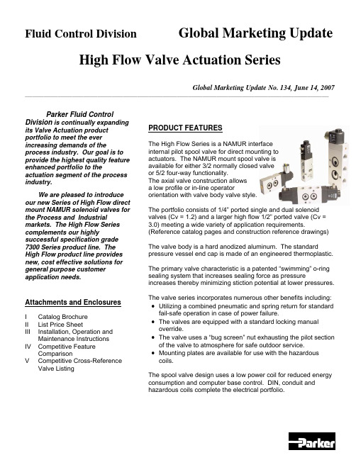
Fluid Control Division Global Marketing Update High Flow Valve Actuation SeriesGlobal Marketing Update No. 134, June 14, 2007 __________________________________________________________________________________________________________________________________ Parker Fluid ControlDivision is continually expanding its Valve Actuation product portfolio to meet the ever increasing demands of the process industry. Our goal is to provide the highest quality feature enhanced portfolio to the actuation segment of the process industry.We are pleased to introduce our new Series of High Flow direct mount NAMUR solenoid valves for the Process and Industrial markets. The High Flow Series complements our highly successful specification grade 7300 Series product line. The High Flow product line provides new, cost effective solutions for general purpose customer application needs.Attachments and EnclosuresI Catalog BrochureII List Price SheetIII Installation, Operation andMaintenanceInstructionsIV Competitive FeatureComparisonV CompetitiveCross-Reference ValveListing PRODUCT FEATURESThe High Flow Series is a NAMUR interfaceinternal pilot spool valve for direct mounting toactuators. The NAMUR mount spool valve isavailable for either 3/2 normally closed valveor 5/2 four-way functionality.The axial valve construction allowsa low profile or in-line operatororientation with valve body valve style.The portfolio consists of 1/4” ported single and dual solenoid valves (Cv = 1.2) and a larger high flow 1/2” ported valve (Cv = 3.0) meeting a wide variety of application requirements. (Reference catalog pages and construction reference drawings)The valve body is a hard anodized aluminum. The standard pressure vessel end cap is made of an engineered thermoplastic.The primary valve characteristic is a patented “swimming” o-ring sealing system that increases sealing force as pressure increases thereby minimizing stiction potential at lower pressures. The valve series incorporates numerous other benefits including: •Utilizing a combined pneumatic and spring return for standard fail-safe operation in case of power failure.•The valves are equipped with a standard locking manual override.•The valve uses a “bug screen” nut exhausting the pilot section of the valve to atmosphere for safe outdoor service.•Mounting plates are available for use with the hazardous coils.The spool valve design uses a low power coil for reduced energy consumption and computer base control. DIN, conduit and hazardous coils complete the electrical portfolio.Global Marketing Update No. 134, June 14, 2007 __________________________________________________________________________________________________________________________________ OPERATION FUNCTIONALITY3/2 Single Solenoid (4 ported, 2 position)NAMUR valve, solenoid operated, for 3-way normally closed operation. In case of an electrical or air failure, valve returns to a fail-safe position through pneumatic and assisted spring return.5/2 Single Solenoid (5 ported, 2 position)NAMUR valve solenoid operated, for 4-way, 2 position operation. In case of an electrical or air failure, valve returns to a fail-safe position through pneumatic and assisted spring return.5/2 Dual Solenoid (5 ported, 2 position)NAMUR valve used for 4-way, 2-position operation. In case of an electrical or air failure, valve “fails as is”. Therefore, valve remains in last position upon failure and will not return to a predetermined position.5/3 Dual Solenoid, Center Position Closed (5 ported, 2 position)NAMUR valve used for 4-way, 2-position operation. In case of an electrical or air failure, the spool returns to the center position thereby removing pressure to the cylinder ports.TECHNICAL PRODUCT CHARACTERISTICSThe new line of valve actuation products offer many features and benefits as follows:Modular construction – Facilitates use of various body configurations and coil options.Mounting Configurations - Direct mount NAMUR pattern with axial operator orientation for single and dual solenoid models for low profile mounting requirements.Manual Override – Standard on all models for manual valve operation during start-up and diagnostic procedures.7mm (1.2Cv ) and 12mm (3.0 Cv) orifice sizes – Multiple sizes to meet various application demands to ensure the solenoid valve is properly sized.Body Materials - Lightweight anodized aluminum.Spool Design – Stainless steel with NBR sealing materials.Exhaust Pilot Cap– Protected pilot sleeve exhaust using “Bug Screen” nut. Helps protect against plugging, dirt, and insects, etc.Ratings – Meets pressures up to 150 psi.Ambient Temperatures – From 14°F (-10°C) to 122°F (50°C), serving most temperature environments. Fluid Temperatures – From 32°F (0°C) to 104°F (40°C).COIL PRODUCT CHARACTERISTICSA selection of low power encapsulated coils as follows:•DIN coil - with 3-pin DIN 43650 type B plug.•Conduit - 3-wire coil.•Hazardous – 3-wire coil with FM and CSA agency approvals meeting Class 1, Groups A,B,C,D and Class II, Groups E,F,G. Meets EEx m II T4 Division 1 requirements.NAMUR INTERFACEMany actuator manufacturers utilize a common mounting pattern referred to as a NAMUR interface for mounting configurations of solenoid valves.The actuator interface dimensions for NAMUR mounting of the pilot valve to the actuator is shown below (dimensions in millimeters).MATERIALS OF CONSTRUCTIONBody: Anodized AluminumEnd Covers: Thermoplastic – Glass-Filled Polyamid 6/6Plunger: 430 Stainless SteelCore Tube: 304 Stainless SteelSteelSprings: StainlessSeals: NBRCages: Polyamide Filled ThermoplasticSteelSpool: StainlessShading Rings: CopperMOUNTING BOLTSThe standard NAMUR interface includes (2) mounting bolts to mount the valve on to the actuator, a positioning stud and two O-rings seals.MOUNTING PLATESDue to the increased width of the hazardous coil to comply with FM and CSA certifications, a mounting plate must be installed as shown in the photograph.The mounting plate kit contains the plate, 2 o-rings, and 2 longer mounting screws.For the ¼” port valve, order kit N60001. For the ½ “ port valve, order kit N60002.ElectricalStandard voltages and voltage code:VOLTAGE CODE 12VDC A 24VDC B 120/60 C 240/60 D 24/60 E 120/50-60 F 240/50-60 GSolenoid Coil SpecificationsThe electrical portfolio is comprised of general purpose class F DIN coil per 43650B and conduit class H coils rated for NEMA classification Types, 1, 2, 3, 3S, 4, 4X. In addition, the hazardous location class H coil is rated for NEMA classification Types 7 and 9; Class I, Divisions 1 and 2, Groups A,B,C,D and Class II, Division 1, Groups E,F,G. The coils are rated for continuous duty application demands.The electrical selector table summarizes each coil specification:Coil Type Coil Part Number Class Protection Construction Agency22mm DINND1x F DIN connector needed for IP65 protection Per DIN 43650B epoxy moldedUL,CSA Conduit –Ordinary locationNC1x H Type 1,2,3,3S,4,4X Epoxy molded, ½ inch NPT conduit None Conduit –Hazardous locationNH1xHType 4X,7,9½ inch NPT conduitCSA,FMCOMPETITIVE FEATURES AND BENEFITSThe primary valve characteristic is a patented “swimming” o-ring sealing system that increases sealing force as pressure increases thereby minimizing stiction potential at lower pressures.The diagram shows a typical cross section view of the valve.valve-head to keep moisture out in brass or in stainless steel available on request, only in combination with alu-head Spool in stainless steel, other inner-parts made from brass, NBR, POM stainless steel Fiber-enforced PA-head, aluminium-version on request 360° turnable,Date CodePRODUCT LABELINGValves are sold in either:• A modular format ordering pressure vessel and coil separately. • Fully assembled with coil assembled to pressure vessel.In either case, the pressure vessel valve body provides the valve identification information defining the valve part number, performance rating and date code. Sample pressure vessel markingCoils will be marked with the appropriate part number, voltage and wattage, and agency information.Sample coil markingAll valves will be packaged with an installation, operation and maintenance instruction sheet indicating conformity with the CE Mark.ORDERING INFORMATIONPRODUCT OFFERINGReference the enclosed catalog brochure (Attachment I) describing the High Flow Series product offering. The catalog pages describe the valve features, general specifications, valve and electrical selection guide, dimensional drawings, and ordering information.PRICINGPressure Vessel list prices for the High Flow NAMUR Series valves are shown in Attachment II. ORDERING INFORMATIONThe Series uses a simple valve number to identify each model. The valves are available fully assembled or in modular form allowing application flexibility in electrical selection. The electrical parts can also be purchased in modular form.Reference the enclosed catalog pages.•When purchasing individual pressure vessels, select the pressure vessel shown on the catalog page and associated list price.•When ordering electrical parts, select the electrical part and associated list price for standard voltages.•When ordering complete valves, add the list price of each component to determine the complete list price for the fully assemble valve selected.The voltage code is the last character of the fully assembled valve or electrical part selected. For example, selecting a single solenoid, 5/2 configuration, 120/60 DIN coil, the complete valve number is:U341N03 + ND1FAVAILABILITY AND DELIVERYParker Fluid Control Division plans to maintain an appropriate service level of finished goods stock to meet business demand of the following NAMUR mount valves. If finished goods stock is available, units will be shipped within 5 business days from receipt of order for order quantities of 25 units or fewer:Product Class 1 Items:U331N03U341N03ND1B, ND1F, ND1G - 24vdc, 120vac, 240vacNC1B, NC1F, NC1G - 24vdc, 120vac, 240vacNH1B, NH1F, NH1G - 24vdc, 120vac, 240vacProduct Class 4 Items - the estimated lead-time (subject to change) is 4 weeks from receipt of order.U347N03U342N03U331N04U341N04ND1A - 12vdcNC1A - 12vdcNH1A - 12vdcAs always, for larger customer orders requiring shorter lead-times, Parker Fluid Control Division will work jointly with each customer by establishing finished goods items to meet customer provided forecasts.DISCOUNTSParker Fluid Control Division’s standard published discounts apply. Current terms and conditions apply for the product.SERVICERETURNSParker Fluid Control Division’s standard return policy applies.REPAIR PARTSParker Fluid Control Division is NOT offering component repair kits for field service at this time. Since the valve is a small, cost effective product, industry experience shows the process markets will replace the complete valve rather than rebuild the valve in the field.INSTALLATION OPERATION AND MAINTENANCE (IOM)An IOM has been created describing valve operation, installation and mounting instructions, maintenance, and troubleshooting procedures for the high flow Series NAMUR valves. Reference Attachment III, IOM HN01.WARRANTYParker Skinner’s standard 2 year warranty policy applies to the pressure vessel, coil and enclosures.PROMOTIONPromotional materials have been prepared to expedite introduction into the market place.CATALOG / LITERATURE• A new catalog has been created containing the features, specifications and outline drawings of the high flow Series valves.• A product launch announcement containing product introduction materials and detailed competitor information will be distributed to each Territory Sales Manager.TRAINING•Each Territory Sales Manager should contact their respective Fluid Control Division Authorized Distributor and Valve Actuation Accounts to arrange training.•The new high flow Series valves will be included in Fluid Control Division’s Valve Actuation Training Program.•Samples of the new high flow Series actuation valves will be provided upon receipt with a complete sample request form following standard Skinner Valve ™ sample procedures.PHASE-OUT OF 2340, 3300 and 7341 Series Product LinesThe introduction of the new product line has resulted in significant product overlap with the 2340, 3300 and 7341 series valves. Therefore, we are taking the following actions to phase out these product lines. Due to the low volume of many of the products, the old families will be replaced by the new High Flow NAMUR valve as follows:The Phase In – Phase Out schedule will begin upon introduction of the new High Flow NAMUR valve. It may be possible to order a specific older model until current inventory is fully depleted at which time the old product will no longer be available. Parker reserves the right to discontinue the old products sooner if conditions warrant.COMPETITIVE REVIEWReference Competitive Feature Comparison of select valves in Attachment IV. The attachment contains a broad selection of valves representative of the competitive offering.Attachment V provides a competitive cross-reference part number listing based on available information for the individual competitors.ASCO is considered the market leader for actuation valves. Other primary competitors include Versa, Automatic, and Herion.Below is a general description of the competitive product offerings.ASCOThe ASCO 8551 Series offers a product line of NAMUR and pipe mount versions. The portfolio consists of pad mount valves with various operator configurations with single and dual solenoids.In general, the ASCO 8551 Series consists of:•Anodized aluminum and stainless steel body using resilient spool construction. •Convertible 3-way and 4-way models based on the newer version. The older version consists of non-convertible 3-way and 4-way models that are similar to the 7300 Series. •20/35 to 150 psi operating pressure differential.•Single and dual solenoid, vertical and axial operator models available.•Cv 0.50 to 0.86.•AC versions from 2.5 watts to 10.1 watts.DC versions from 3.0 watts to 11.6 watts.•DIN, watertight and explosion solenoids available based on model.The Parker High Flow Series NAMUR mount valves are specified to meet the application requirement. A conversion or mounting plate is not required when using a DIN coil. The valve mounts directly to the actuator in a very cost-effective and efficient manner.VersaVersa offers a series of valves for process control markets including applications for pneumatic actuators and 316 stainless valves for corrosive requirements. The valve offering consists of NAMUR, body ported, lockout valves, latching and manual reset valves and redundant solenoid valves.Specific to the actuation area, Versa offers a convertible 3-way / 4-way version and direct acting 3-way pad mount valve. Available options include Intrinsically Safe, Low power and CENELEC flameproof enclosures.•3/2, 5/2 port plug versions. Valves field convertible by relocating a port plug converting from 3-way to 4-way or 4-way to 3-way.•Anodized aluminum, stainless steel and brass body using resilient spool construction. •Single and dual solenoid models (5/2) and dual solenoid centered position (5/3) with standard manual override.•15 to 115 psi operating pressure, Cv 0.75.•DIN, conduit and explosion solenoids available based on model.•8.5 watt AC, 10.5 watt DC.•Class A or F insulation.Automatic Valve Co. (AVC)They are considered the low price player in the market. They offer a NAMUR mount COMPACT Series. The series has limited options, but offers the ability to order valves with the solenoid on the left or right side.•3/2, 5/2 port plug versions, 1/4” npt porting only.•Anodized aluminum body using resilient spool construction.•40 to 150 psi operating pressure differential, Cv 1.0.•NEMA 4 and 7 solenoids, remote air and manual operators.•DIN, conduit and explosion solenoids available based on model, coil ratings to Class H. Herion•3/2, 5/2 port plug versions, NAMUR mount, 1/8” NPT, ¼” NPT, ½” NPT.•Anodized aluminum body using resilient spool construction.•25 to 150 psi operating pressure differential, Cv 1.1 to 1.4.•NEMA 4 and 7 solenoids, manual operators.•Low power coils available at reduced ratings.•DIN, conduit and explosion solenoids available based on models.•Locking and momentary manual override available.•Requires spacer plate for hazardous coil.Max-Air TechnologyU.S. division of M Technology Srl located in Italy. Also offer rack & pinion actuators and position indicators and mechanical switches that can be assembled as a complete unit.•3/2, 5/2 port plug versions, 1/4” npt porting only.•Epoxy coated aluminum body with plated spool. And standard manual override.•DIN and explosion solenoids available based on model, Class F standard, Class H optional. •Uses a pop-up air indicator located in pilot section to indicate if the solenoid valve is pressurized.•Optional IS and ATEX DIN coil construction.Q&A SESSIONQ? Why did we introduce the High Flow NAMUR Series valve product line?The principle reason for introducing the valve line is to meet increasing market demands for smaller, cost effective valve models for the process valve actuation markets. The Parker 7300 Series valve line offers a high-end specification grade product in multiple bodymaterials to meet general purpose ordinary requirements to the most stringent application requirements. Also, the 2340 series of aluminum body valves lacked a suitable hazardous coil limiting application potentials.The new product line overcomes the 2340 series deficiencies at a most competitive price for general purpose application requirements. The portfolio includes expanded models with higher flow factors for larger actuator designs. The new line includes a 1/2” namur valve to accommodate the trend toward larger actuators and higher flows.Finally, we’re continuing our strategic thrust in the process markets with a new product offering and responding to competitive product positions.Q? Will the High Flow Series product line replace the 2340 Series and 3300 Series valves?In a word, yes. First, since the introduction of the 2340 series and 3300 series valves(dating back to the late ‘90’s), many changes have taken place in the market. The general purpose ordinary location market generally does not require the high technical or safety standards found in these product lines. Due to deficiencies in the former product lines, specifically the lack of a hazardous coil, we were not able to meet the availability and price competitiveness. The current product lines are focused toward higher technicalrequirements resulting in low-volume market segments and overlap price-wise with the 7300 Series valve lines. To reduce complexity and offer a simplified, cost-effective processactuation valve line, the 2340 catalog portfolio will (eventually) be phased-out.Q? Describe the comparison to the 7300 product line.The High Flow Series offers similar product features and benefits compared to the 7300 Series, in particular:• Total modularity.•Interchangeable electrical parts.•Unique spool designs to eliminate risk of sticking.•High quality in proven valve designs.•Standard manual override.The distinctive features of the High Flow Series compared to the 7300 Series include:• Smaller physical size.•More cost effective compared to 7300 with manual override (for certain type application needs).Q? Where must the 7300 series valves be used versus the new line?The 7300 series contains features, multiple operator configurations and electrical coilsappropriate for more demanding critical applications including:•Higher flows appropriate for higher actuator torque specifications.•Intrinsically Safe (IS) and ultra low power environmental conditions.•Manual reset options used as a safety device on solenoid valves to prevent process resumption without manually resetting each valve.•Low temperatures application demands of –40°F/C.•Field convertible manual overrides including locking and momentary requirements. Q? Will a conversion plate eventually become available?The product line contains individual 3-way and 4-way valve configuration. When utilizing a DIN coil, this method provides the most cost-effective, competitive solution. Granted, whilea conversion plate offers the benefit of using one style valve, it also adds significant andunnecessary costs. Since the valve is focused and priced to pursue higher volumerequirements, the valve functionality will be known.。
Compumotor Z635 电机用户指南说明书

U S E R G U I D E C H A N G E S U M M A RYThe following is a summary of the primary changes to this user guide sincethe last version was released. This user guide, version 88-010759-01H,supersedes version 88-010759-01G.The entire user guide has been changed according to the new Compumotoruser guide styles, format, and illustration standards. Also, the chapters havebeen renumbered and reorganized. Technical changes to each chapter aresummarized below.ChapterIntroductionThe Z635 motor was added to the “What You Should Have” section.ChapterGetting StartedChapter was unchanged.Chapter Installation t Installation (wiring) directions were provided for the Brake (-B) Braking option. t Maximum step rate was corrected (was 2.5 MHz, changed to 1 MHz). See STEP Input.t The DIRECTION Input schematic was modified.ChapterApplicationDesignChapter was unchanged.ChapterZ Series Shunt Regulator The capacitor energy absorption calculation was modified (refer to “Selecting a Z Series Shunt Regulator.”)Chapter Software Reference In the CTC command description, time increments were corrected from ms to µs.Chapter Hardware Reference An exception for Z600 and Z900 Series motors was added regarding the IP Classification. The shaft is IP30 rated (not IP65).ChapterMaintenance &TroubleshootingChapter was unchanged.T A B L E O F C O N T E N T S How To Use This User Guide (iii)Assumptions (iii)Installation Process Overview (iii)Installation Procedures (iii)Contents of This User Guide (iii)Related Publications (iv)À INTRODUCTION (1)Product Description (1)Product Features (2)Interface Options (2)Theory of Operation (2)` GETTING STARTED (5)What You Should Have (5)Drive/Motor Configuration (5)Check-Out Procedure (6)Tools (6)Position Mode (11)Torque Mode (12)Velocity Mode (13)´ INSTALLATION (15)Environmental Considerations (15)Complete System Configurations (15)Drive Mounting (15)Panel Layout (17)Motor Mounting (17)System Wiring (29)Connections (29)Resolver Connections (31)Indexer Connections (31)Indexer Connector Outputs (34)I/O[1] Connections (35)I/O[2] Connections (39)Line Power Connections (39)Check-Out Procedure (41)ˆ APPLICATION DESIGN (43)Basic Servo Tuning Theory (43)Servo Tuning (46)47 Alphanumeric Display and Pushbuttons...........................................................................................Tuning in Different Modes of Operation (49)Position Mode (50)Torque Mode (50)Velocity Mode (51)Pseudo-Quadrature Outputs (53)55˜ Z SERIES SHUNT REGULATOR.....................................................................................................What Is A Shunt Regulator? (55)Shunt Regulator Installation (55)Selecting a Z Series Shunt Regulator (56)Contents i¯ SOFTWARE REFERENCE (61)Command Format Description (61)Command Identifier (61)Command name (61)Version (62)Characteristics (62)Attributes (63)Description (63)Example (63)Command List (64)Alphabetical Command List (65)˘ HARDWARE REFERENCE (85)Z600 Electrical Specifications (85)Input Power (85)Output Power (85)Z600 Motor/Drive Configuration (85)Z600 Technical Data (86)Positional Repeatability (86)Positional Accuracy (86)Motor/Drive Compatibility (86)Motor Brakes (86)Motor Data (86)Speed/Torque Curves (94)Z800 Electrical Specifications (96)Input Power (96)Output Power (96)Z800 Motor/Drive Configuration (96)Z800 Technical Data (96)Positional Repeatability (97)Positional Accuracy (97)Motor/Drive Compatibility (97)Motor Brakes (97)Motor Data (97)Speed/Torque Curves (104)Z900 Electrical Specifications (106)Input Power (106)Output Power (106)Z900 Motor/Drive Configuration (106)Z900 Technical Data (106)Positional Repeatability (107)Positional Accuracy (107)Motor Drive Compatibility (107)Motor Brakes (107)Motor Data (107)Speed/Torque Curves (112)113˙ MAINTENANCE & TROUBLESHOOTING.....................................................................................Motor Maintenance (113)Drive Maintenance (113)Troubleshooting (113)Diagnostic LEDs (114)Drive Warning (114)Drive Faults (115)RS-232C Problems (116)Returning The System (116)APPENDIX (117)Alphabetical Command List (117)INDEX (119)ii Z Drive User GuideHow To Use This User GuideThis user guide is designed to help you install, develop, and maintain yoursystem. Each chapter begins with a list of specific objectives that should bemet after you have read the chapter. This section should help you find anduse the information in this user guide.AssumptionsThis user guide assumes that the user has a fundamental understanding ofthe following information.t Basic electronic concepts (voltages, switches, current, etc.)t Basic motion control concepts (torque, velocity, distance, force, etc.) Installation Process OverviewTo ensure trouble-free operation, you should pay special attention to theenvironment in which the Z Drive equipment will operate. Environmentalconditions include the layout, mounting, and wiring and grounding practicesused. These recommendations are intended to help you easily and safelyintegrate the Z Drive into your facility.Installation ProceduresBefore you attempt to install this product, you should complete the followingsteps:Review this user guide. Become familiar with the user guide's contents so thatyou can quickly find the information you need.Develop a basic understanding of all system components, their functions, andinterrelationships.After you have read Chapter and clearly understand what must be done toproperly install the system, begin the installation process. Do not deviate fromthe sequence or installation methods provided.Before you customize your system, check all of the system functions andfeatures to ensure that you have completed the installation process correctly.The successful completion of these steps will prevent subsequentperformance problems and allow you to isolate and resolve any potentialsystem difficulties before they affect your system.Contents of This User GuideThis user guide contains the following information.Chapter : Introduction This chapter provides a description of the product and a brief account of its features.Chapter : Getting Started This chapter contains a detailed list of items you should have received with your Z Drive shipment. It will help you become familiar with the system and ensure that each component functions properly.Chapter : Installation This chapter provided instructions for you to properly mount the system and make all electrical and non-electrical connections. Upon completion of this chapter, your system should be completely installed and ready to perform basic operations.Chapter : Application Design This chapter provides additional information that will help you customize the system to meet your application's needs. Important application considerations are discussed. Sample applications are provided.Chapter : Software Reference This chapter describes the Z Drive's set-up commands. These commands allow you to set system parameters, tune the drive, and display drive status.Chapter : Z Series Shunt Regulator This chapter contains information on the shunt regulator option for the Z Drive. Installation instructions, dimensions, and selection criteria (400W version vs. 800W version) are included.Contents iiiChapter : Hardware Reference This chapter contains information on system specifications (dimensions and performance). This chapter may be used as a quick-reference tool for proper I/O connections.Chapter : Maintenance & Troubleshooting This chapter describes Compumotor's recommended system maintenance procedures. It also provides methods for isolating and resolving hardware and software problems. Diagnostic error codes are listed.Related PublicationsThe following publications may be helpful resources.Seyer, Martin. RS-232C Made Easy: Connecting Computers, Printers, Terminalsand Modems. Englewood Cliffs, New Jersey: Prentice Hall, Inc., 1984Current Parker Compumotor Motion Control CatalogManual for the IBM or IBM-compatible computer that you may use with the Z DriveSchram, Peter (editor). The National Electric Code Handbook (Third Edition).Quincy, MA: National Fire Protection Associationiv Z Drive User GuideC H A P T E RIntroduction The information in this chapter will enable you to:t Understand the product's basic functions, features, and theory of operation Product DescriptionThe Z Drive is a brushless servo system that includes a brushlessservomotor, a brushless resolver (for feedback), and a Digital SignalProcessor (DSP) based servo amplifier. Digital electronics simplify systemoperation and maintenance.The Z Drive can accept either a digital (Step and Direction) input or ananalog (±10V) input. You can configure the Z Drive to servo on commandedposition, velocity, or torque. The series offers maximum speeds of 7000 rpm,maximum continuous torques of 9000 oz-in, and maximum peak torques of18000 oz-in.The Z Drive uses two processors to achieve high-performance servo control.The first processor (DSP) compares the commanded inputs (position,velocity, or torque) to the resolver feedback, and then determines the propermotor currents to apply. The second processor handles all usercommunication, error checking, and additional I/O. All servo performanceparameters are stored in battery-backed RAM (random access memory).Z Drive systems can be installed and operated easily with minimal trainingin servo systems. Z Series motor/drives are supplied as packaged systemsthat are factory compensated for typical load and performancerequirements. In most applications, no adjustments will be required. Whenadjustments are required, changes to the drive can be made from twointerfaces—push-button adjustments or an RS-232C interface. Theseinterfaces provide access to all servo parameters simply and effectively.The Z Drive's power amplifier uses a bipolar 7 kHz pulse-width modulation(PWM) sinusoidal current control scheme. This type of amplifier improvesreliability, power regulation, and low-speed smoothness.Chapter Introduction1Product Featurest Brushless servo motort Brushless resolver feedbackt Speeds to 7000 rpmt Torques to 9000 oz-in continuous (18000 oz-in peak)t User programmable resolutions (200 - 65536 steps/rev, 5000 steps/rev standard)t Multi-processor control: no drift, no analog pots to adjustt Fan-cooled compact drive enclosuret7 kHz PWM switching frequencyt Accepts digital step and direction inputst Accepts analog (±10V) input for velocity or torque controlt Analog (±10V) output monitor for either velocity or torquet Pseudo 4096 pulse per revolution (ppr) incremental encoder output forinterfacing with servo controlst Servo parameters factory-set and stored in battery-backed RAM (random accessmemory)t High-noise immunity due to optical isolation and brushless resolver technologyt Simple push-button adjustment of servo gainst Alphanumeric display for fault or user-defined messagest RS-232C interfaceInterface OptionsIn Step and Direction mode, the Z Drive is compatible with all Compumotorindexers. The Z Drive moves the motor one increment in the specifieddirection for each step pulse received. Both of the drive's Step and Directioninputs are optically isolated and can be driven by an external pulsegenerator. The Z Drive's resolution is programmable, so you can specifyconvenient motor increments. The optically isolated analog input accepts a±10V signal that may be configured as either a velocity or torque command.The ZX is the drive/indexer version of the Z Drive. It contains the servocontroller and a complete RS-232C based indexer that executesCompumotor's X Series programming language. You can combine motioncontrol parameters such as distance, velocity, and acceleration intosequences with time delays, loops, and programmable outputs. Thesesequences can be controlled via RS-232C or via external inputs that can beconnected to a PLC or host computer. You can use trigger inputs to coordinateprogram execution with external events. Multiple motion control programscan be stored in nonvolatile memory and executed automatically fromexternal sequence and trigger controls. The X Series language is based onsimple commands, and uses decimal numbers.Theory of OperationThe Z Drive's primary function is to servo to either a digital positioncommand from an indexer or to an analog voltage command (velocity ortorque) from a servo controller.In Position mode, the indexer sends a position command to the drive andthe resolver feeds back the actual position of the shaft. If the actual positionof the shaft is different from the commanded position, a positional error isproduced. The drive then commands torque to the motor to correct thepositional error. In Velocity mode, the servo controller sends a velocitycommand and the drive servos to it by comparing the commanded velocity tothe actual velocity. In Torque mode, the servo controller controls theactual shaft torque directly.2Z Drive User GuideChapter Introduction 3The Z Drive digital servo system is composed of three major components:the servo motor, the drive, and the resolver.Microprocessor-based IndexerSERVO MOTOR RESOLVERA Digital Signal Processor (DSP)Resolver - to -Digital Converter Digital-to-Analog Converter Communication (RS-232C, front panel, I/O)Z Drive Digital Servo SystemThe Z motor family consists of brushless, 3-phase, AC motors. The figure below illustrates the basic construction of the Z servo motor. The permanent magnets are securely held in place by metal bands and composite fiber materials to allow high-speed performance. The rotors are precision-balanced, which provides low- and high-speed smoothness. The windings are located in the outer portion of the motor (stator). This inside-outconstruction allows better heat dissipation than conventional brush-type motors. As a result, higher continuous torque and horsepower ratings are achieved for a given motor size.Stator LaminationStatorWindingsRotorMagnetsS4Z Drive User Guide Controlling the phase of each of the motor's stator currents ensures balanced 3-phase operation and minimizes torque ripple. Actual motor currents are sensed, and the current is adjusted using pulse width modulation. Feedback is provided by a single-speed, brushless, pancake-type resolver.The resolver is mounted directly to the motor shaft. This eliminates the need for internal coupling. The resolver stator windings are mounted to themotor housing.。
635德马吉机床

Fanuc 0i-MC, 20 位刀库带双爪换刀机械手,线性导轨, 废料槽,电子手轮
技术亮点
» 强力主轴 (8,000 rpm / 83 Nm (40% DC) / 13 kW)
» 带快速双爪换刀机械手的 20 刀位刀库
* DMC 1035 V eco 的数据
» 大型加工空间 » 最短的非加工运行时间: 快移速度 25 m/min,
207 368
俯视图
1,800 1,829
1,640 890
42 249
2,500 2,530
2,000 50
max 2,665 (2,380*) 2,818 2,553
350 2,300 2,385
» DMGECOLINE ı 安装图与技术参数
功率图
DMC 635 V eco / 1035 V eco(2)
» DMGECOLINE ı 机床结构与选配 1
2
3
1 带电缆的控制柜 2 X / Y / Z 轴行程直接测量系统包括空气清洗 3 Heidenhain TT 130 刀具探测系统
您的维护标准 » 具有良好畅通性的保养区域 (润滑和气动装置) » 用颜色标志不同媒介导线
» 宽敞且通达性良好的维修门和控制柜门
技术参数
机床型号 工作范围 X 轴行程 Y 轴行程 Z 轴行程 进给 进给力 进给速度 快移 定位精度 Pmax 依据 VDI / DGQ 3441 (间接/直接行程测量系统) Pmax 依据 JIS B6330-1980 (间接/直接行程测量系统) 工作轴 (标配) 最大转速 驱动功率 (40%/100% DC) 扭矩 (40%/100% DC) 刀柄 刀库 / 换刀机械手 (双爪换刀机械手) 刀具数量 最大刀具直径 最大刀具直径 (任意的相邻工位) 最大刀具长度 换刀时间 屑 – 屑换刀时间 工作台规格 带 T 形槽的装夹面积 装料高度 (工作台上沿) 工作台载重 (台面中心承重)
MAX630CSA+中文资料
General DescriptionMaxim’s MAX630 and MAX4193 CMOS DC-DC regula-tors are designed for simple, efficient, minimum-size DC-DC converter circuits in the 5mW to 5W range. The MAX630 and MAX4193 provide all control and power handling functions in a compact 8-pin package: a 1.31V bandgap reference, an oscillator, a voltage com-parator, and a 375mA N-channel output MOSF ET. A comparator is also provided for low-battery detection.Operating current is only 70µA and is nearly indepen-dent of output switch current or duty cycle. A logic-level input shuts down the regulator to less than 1µA quies-cent current. Low-current operation ensures high effi-ciency even in low-power battery-operated systems.The MAX630 and MAX4193 are compatible with most battery voltages, operating from 2.0V to 16.5V.The devices are pin compatible with the Raytheon bipo-lar circuits, RC4191/2/3, while providing significantly improved efficiency and low-voltage operation. Maxim also manufactures the MAX631, MAX632, and MAX633DC-DC converters, which reduce the external compo-nent count in fixed-output 5V, 12V, and 15V circuits.See Table 2 at the end of this data sheet for a summary of other Maxim DC-DC converters.Applications+5V to +15V DC-DC ConvertersHigh-Efficiency Battery-Powered DC-DC Converters+3V to +5V DC-DC Converters 9V Battery Life ExtensionUninterruptible 5V Power Supplies5mW to 5W Switch-Mode Power SuppliesFeatures♦High Efficiency—85% (typ)♦70µA Typical Operating Current ♦1µA Maximum Quiescent Current ♦2.0V to 16.5V Operation♦525mA (Peak) Onboard Drive Capability ♦±1.5% Output Voltage Accuracy (MAX630)♦Low-Battery Detector♦Compact 8-Pin Mini-DIP and SO Packages ♦Pin Compatible with RC4191/2/3MAX630/MAX4193CMOS Micropower Step-UpSwitching Regulator________________________________________________________________Maxim Integrated Products 1Pin ConfigurationOrdering InformationTypical Operating Circuit19-0915; Rev 2; 9/08For pricing, delivery, and ordering information,please contact Maxim/Dallas Direct!at 1-888-629-4642, or visit Maxim’s website at .*Dice are specified at T A = +25°C. Contact factory for dice specifications.**Contact factory for availability and processing to MIL-STD-883.†Contact factory for availibility.M A X 630/M A X 4193CMOS Micropower Step-Up Switching Regulator 2_______________________________________________________________________________________ABSOLUTE MAXIMUM RATINGSELECTRICAL CHARACTERISTICSStresses beyond those listed under “Absolute Maximum Ratings” may cause permanent damage to the device. These are stress ratings only, and functional operation of the device at these or any other conditions beyond those indicated in the operational sections of the specifications is not implied. Exposure to absolute maximum rating conditions for extended periods may affect device reliability.Supply Voltage.......................................................................18V Storage Temperature Range ............................-65°C to +160°C Lead Temperature (soldering, 10s).................................+300°C Operating Temperature RangeMAX630C, MAX4193C........................................0°C to +70°C MAX630E, MAX4193E.....................................-40°C to +85°C MAX630M, MAX4193M..................................-55°C to +125°CPower Dissipation8-Pin PDIP (derate 6.25mW/°C above +50°C).............468mW 8-Pin SO (derate 5.88mW/°C above +50°C)................441mW 8-Pin CERDIP (derate 8.33mW/°C above +50°C)........833mW Input Voltage (Pins 1, 2, 6, 7).....................-0.3V to (+V S + 0.3V)Output Voltage, L X and LBD..................................................18V L X Output Current..................................................525mA (Peak)LBD Output Current............................................................50mAMAX630/MAX4193CMOS Micropower Step-UpSwitching Regulator_______________________________________________________________________________________3L X ON-RESISTANCE vs.TEMPERATURETEMPERATURE (°C)L X R O N (Ω)100755025-25-5024680125SUPPLY CURRENT vs.TEMPERATUREM A X 630/4193 t o c 02TEMPERATURE (°C)I S (μA )100755025-25-50402080601201001400125SUPPLY CURRENT vs.SUPPLY VOLTAGEM A X 630/4193 t o c 03+V S (V)I S (μA )14121086425015010025020030016Typical Operating Characteristics(T A = +25°C, unless otherwise noted.)ELECTRICAL CHARACTERISTICSNote 1:Guaranteed by correlation with DC pulse measurements.Note 2:The operating frequency range is guaranteed by design and verified with sample testing.Detailed DescriptionThe operation of the MAX630 can best be understood by examining the voltage regulating loop of F igure 1.R1 and R2 divide the output voltage, which is com-pared with the 1.3V internal reference by comparator COMP1. When the output voltage is lower than desired,the comparator output goes high and the oscillator out-put pulses are passed through the NOR gate latch,turning on the output N-channel MOSFET at pin 3, L X .As long as the output voltage is less than the desired voltage, pin 3 drives the inductor with a series of pulses at the oscillator frequency.Each time the output N-channel MOSFET is turned on,the current through the external coil, L1, increases,storing energy in the coil. Each time the output turns off,the voltage across the coil reverses sign and the volt-age at L X rises until the catch diode, D1, is forward biased, delivering power to the output.When the output voltage reaches the desired level,1.31V x (1 + R1 / R2), the comparator output goes low and the inductor is no longer pulsed. Current is then supplied by the filter capacitor, C1, until the output volt-age drops below the threshold, and once again L X is switched on, repeating the cycle. The average duty cycle at L X is directly proportional to the output current.Output Driver (L X Pin)The MAX630/MAX4193 output device is a large N-channel MOSFET with an on-resistance of 4Ωand a peak current rating of 525mA. One well-known advan-tage that MOSF ETs have over bipolar transistors in switching applications is higher speed, which reduces switching losses and allows the use of smaller, lighter,less costly magnetic components. Also important is that MOSF ETs, unlike bipolar transistors, do not require base current that, in low-power DC-DC converters,often accounts for a major portion of input power.The operating current of the MAX630 and MAX4193increases by approximately 1µA/kHz at maximum power output due to the charging current required by the gate capacitance of the L X output driver (e.g., 40µA increase at a 40kHz operating frequency). In compari-son, equivalent bipolar circuits typically drive their NPN L X output device with 2mA of base drive, causing the bipolar circuit’s operating current to increase by a fac-tor of 10 between no load and full load.OscillatorThe oscillator frequency is set by a single external, low-cost ceramic capacitor connected to pin 2, C X . 47pF sets the oscillator to 40kHz, a reasonable compromise between lower switching losses at low frequencies and reduced inductor size at higher frequencies.M A X 630/M A X 4193CMOS Micropower Step-Up Switching Regulator 4_______________________________________________________________________________________Low-Battery DetectorThe low-battery detector compares the voltage on LBR with the internal 1.31V reference. The output, LBD, is an open-drain N-channel MOSFET. In addition to detecting and warning of a low battery voltage, the comparator can also perform other voltage-monitoring operations such as power-failure detection.Another use of the low-battery detector is to lower the oscillator frequency when the input voltage goes below a specified level. Lowering the oscillator frequency increases the available output power, compensating for the decrease in available power caused by reduced input voltage (see Figure 5).Logic-Level Shutdown InputThe shutdown mode is entered whenever I C (pin 6) is driven below 0.2V or left floating. When shut down, theMAX630’s analog circuitry, oscillator, L X , and LBD out-puts are turned off. The device’s quiescent current dur-ing shutdown is typically 10nA (1µA max).Bootstrapped OperationIn most circuits, the preferred source of +V S voltage for the MAX630 and MAX4193 is the boosted output volt-age. This is often referred to as a “bootstrapped” oper-ation since the circuit figuratively “lifts” itself up.The on-resistance of the N-channel L X output decreas-es with an increase in +V S ; however, the device operat-ing current goes up with +V S (see the Typical Operating Characteristics , I S vs. +V S graph). In circuits with very low output current and input voltages greater than 3V, it may be more efficient to connect +V S direct-ly to the input voltage rather than bootstrap.MAX630/MAX4193CMOS Micropower Step-UpSwitching Regulator_______________________________________________________________________________________5Figure 1. +5V to +15V Converter and Block DiagramM A X 630/M A X 4193External ComponentsResistorsSince the LBR and V FB input bias currents are specified as 10nA (max), the current in the dividers R1/R2 and R3/R4 (Figure 1) may be as low as 1µA without signifi-cantly affecting accuracy. Normally R2 and R4 are between 10k Ωand 1M Ω, which sets the current in the voltage-dividers in the 1.3µA to 130µA range. R1 and R3 can then be calculated as follows:where V OUT is the desired output voltage and V LB isthe desired low-battery warning threshold.If the I C (shutdown) input is pulled up through a resistor rather than connected directly to +V S , the current through the pullup resistor should be a minimum of 4µAInductor ValueThe available output current from a DC-DC voltageboost converter is a function of the input voltage, exter-nal inductor value, output voltage, and the operating frequency.The inductor must 1) have the correct inductance, 2) be able to handle the required peak currents, and 3) have acceptable series resistance and core losses. If the inductance is too high, the MAX630 will not be able to deliver the desired output power, even with the L X out-put on for every oscillator cycle. The available output power can be increased by either decreasing the inductance or the frequency. Reducing the frequency increases the on-period of the L X output, thereby increasing the peak inductor current. The available out-put power is increased since it is proportional to the square of the peak inductor current (I PK ).where P OUT includes the power dissipated in the catchdiode (D1) as well as that in the load. If the inductance is too low, the current at L X may exceed the maximum rating. The minimum allowed inductor value is expressed by:where I MAX ≈525mA (peak L X current) and t ON is the on-time of the L X output.The most common MAX630 circuit is a boost-mode converter (Figure 1). When the N-channel output device is on, the current linearly rises since:At the end of the on-time (14µs for 40kHz, 55% duty-cycle oscillator) the current is:The energy in the coil is:At maximum load, this cycle is repeated 40,000 timesper second, and the power transferred through the coil is 40,000 x 5.25 = 210mW. Since the coil only supplies the voltage above the input voltage, at 15V, the DC-DC converter can supply 210mW / (15V - 5V) = 21mA. The coil provides 210mW and the battery directly supplies another 105mW, for a total of 315mW of output power. If the load draws less than 21mA, the MAX630 turns on its output only often enough to keep the output voltage at a constant 15V.Reducing the inductor value increases the available output current: lower L increases the peak current,thereby increasing the available power. The external inductor required by the MAX630 is readily obtained from a variety of suppliers (Table 1). Standard coils are suitable for most applications.Types of InductorsMolded InductorsThese are cylindrically wound coils that look similar to 1W resistors. They have the advantages of low cost and ease of handling, but have higher resistance, higher losses, and lower power handling capability than other types.102112131131104134131131ΩΩΩΩ≤≤=−≤≤=− .. ..R M R R x V VR M R R x V VOUTLBCMOS Micropower Step-Up Switching Regulator 6_______________________________________________________________________________________Potted Toroidal InductorsA typical 1mH, 0.82Ωpotted toroidal inductor (Dale TE-3Q4TA) is 0.685in in diameter by 0.385in high and mounts directly onto a PC board by its leads. Such devices offer high efficiency and mounting ease, but at a somewhat higher cost than molded inductors.Ferrite Cores (Pot Cores)Pot cores are very popular as switch-mode inductors since they offer high performance and ease of design.The coils are generally wound on a plastic bobbin,which is then placed between two pot core sections. A simple clip to hold the core sections together com-pletes the inductor. Smaller pot cores mount directly onto PC boards through the bobbin terminals. Cores come in a wide variety of sizes, often with the center posts ground down to provide an air gap. The gap pre-vents saturation while accurately defining the induc-tance per turn squared.Pot cores are suitable for all DC-DC converters, but are usually used in the higher power applications. They are also useful for experimentation since it is easy to wind coils onto the plastic bobbins.Toroidal CoresIn volume production, the toroidal core offers high per-formance, low size and weight, and low cost. They are,however, slightly more difficult for prototyping, in that manually winding turns onto a toroid is more tedious than on the plastic bobbins used with pot cores.Toroids are more efficient for a given size since the flux is more evenly distributed than in a pot core, where the effective core area differs between the post, side, top,and bottom.Since it is difficult to gap a toroid, manufacturers produce toroids using a mixture of ferromagnetic powder (typically iron or Mo-Permalloy powder) and a binder. The perme-ability is controlled by varying the amount of binder,which changes the effective gap between the ferromag-netic particles. Mo-Permalloy powder (MPP) cores have lower losses and are recommended for the highest effi-ciency, while iron powder cores are lower cost.DiodesIn most MAX630 circuits, the inductor current returns to zero before L X turns on for the next output pulse. This allows the use of slow turn-off diodes. On the other hand, the diode current abruptly goes from zero to full peak current each time L X switches off (Figure 1, D1).To avoid excessive losses, the diode must therefore have a fast turn-on time.F or low-power circuits with peak currents less than 100mA, signal diodes such as 1N4148s perform well.For higher-current circuits, or for maximum efficiency at low power, the 1N5817 series of Schottky diodes are recommended. Although 1N4001s and other general-purpose rectifiers are rated for high currents, they are unacceptable because their slow turn-on time results in excessive losses.MAX630/MAX4193CMOS Micropower Step-UpSwitching Regulator_______________________________________________________________________________________7Table 1. Coil and Core ManufacturersM A X 630/M A X 4193Filter CapacitorThe output-voltage ripple has two components, with approximately 90 degrees phase difference between them. One component is created by the change in the capacitor’s stored charge with each output pulse. The other ripple component is the product of the capacitor’s charge/discharge current and its effective series resis-tance (ESR). With low-cost aluminum electrolytic capacitors, the ESR-produced ripple is generally larger than that caused by the change in charge.where V IN is the coil input voltage, L is its inductance, f is the oscillator frequency, and ESR is the equivalent series resistance of the filter capacitor.The output ripple resulting from the change in charge on the filter capacitor is:where t CHG and t DIS are the charge and dischargetimes for the inductor (1/2f can be used for nominal cal-culations).Oscillator Capacitor, C XThe oscillator capacitor, C X , is a noncritical ceramic or silver mica capacitor. C X can also be calculated by:where f is the desired operating frequency in Hertz, and C INT is the sum of the stray capacitance on the C X pin and the internal capacitance of the package. The internal capacitance is typically 1pF for the plastic package and 3pF for the CERDIP package. Typical stray capacitances are about 3pF for normal PC board layouts, but will be significantly higher if a socket is used.Bypassing and CompensationSince the inductor-charging current can be relatively large, high currents can flow through the ground con-nection of the MAX630/MAX4193. To prevent unwanted feedback, the impedance of the ground path must be as low as possible, and supply bypassing should be used for the device.When large values (>50k Ω) are used for the voltage-setting resistors, R1 and R2 of F igure 1, stray capaci-tance at the V FB input can add a lag to the feedback response, destabilizing the regulator, increasing low-frequency ripple, and lowering efficiency. This can often be avoided by minimizing the stray capacitance at the V FB node. It can also be remedied by adding a lead compensation capacitor of 100pF to 10nF in paral-lel with R1 in Figure 1.DC-DC Converter ConfigurationsDC-DC converters come in three basic topologies:buck, boost, and buck-boost (Figure 2). The MAX630 is usually operated in the positive-voltage boost circuit,where the output voltage is greater than the input.The boost circuit is used where the input voltage is always less than the desired output and the buck circuit is used where the input is greater than the output. Thebuck-boost circuit inverts, and can be used with, inputCMOS Micropower Step-Up Switching Regulator 8_______________________________________________________________________________________Figure 2. DC-DC Converter Configurationsvoltages that are either greater or less than the output. DC-DC converters can also be classified by the control method. The two most common are pulse-width modu-lation (PWM) and pulse-frequency modulation (PF M). PWM switch-mode power-supply ICs (of which current-mode control is one variant) are well-established in high-power off-line switchers. Both PWM and PF M cir-cuits control the output voltage by varying duty cycle. In the PWM circuit, the frequency is held constant and the width of each pulse is varied. In the PFM circuit, the pulse width is held constant and duty cycle is con-trolled by changing the pulse repetition rate.The MAX630 refines the basic PFM by employing a con-stant-frequency oscillator. Its output MOSFET is switched on when the oscillator is high and the output voltages is lower than desired. If the output voltage is higher than desired, the MOSFET output is disabled for that oscillator cycle. This pulse skipping varies the average duty cycle, and thereby controls the output voltage.Note that, unlike the PWM ICs, which use an op amp as the control element, the MAX630 uses a comparator tocompare the output voltage to an onboard reference. This reduces the number of external components and operating current.Typical Applications+5V to +15V DC-DC Converter Figure 1 shows a simple circuit that generates +15V at approximately 20mA from a +5V input. The MAX630 has a ±1.5% reference accuracy, so the output voltage has an untrimmed accuracy of ±3.5% if R1 and R2 are 1% resistors. Other output voltages can also be select-ed by changing the feedback resistors. Capacitor C X sets the oscillator frequency (47pF = 40kHz), while C1 limits output ripple to about 50mV.With a low-cost molded inductor, the circuit’s efficiency is about 75%, but an inductor with lower series resis-tance such as the Dale TE3Q4TA increases efficiency to around 85%. A key to high efficiency is that the MAX630 itself is powered from the +15V output. This provides the onboard N-channel output device with 15V gate drive, lowering its on-resistance to about 4Ω. When +5V power is first applied, current flows through L1 and D1, supplying the MAX630 with 4.4V for startup.+5V to ±15V DC-DC Converter The circuit in F igure 3 is similar to that of F igure 1 except that two more windings are added to the induc-tor. The 1408 (14mm x 8mm) pot core specified is an IEC standard size available from many manufacturers (see Table 1). The -15V output is semiregulated, typi-cally varying from -13.6V to -14.4V as the +15V load current changes from no load to 20mA.2.5W, 3V to 5V DC-DC ConverterSome systems, although battery powered, need high currents for short periods, and then shut down to a low-power state. The extra circuitry of Figure 4 is designed tomeet these high-current needs. Operating in the buck-boost or flyback mode, the circuit converts -3V to +5V.The left side of Figure 4 is similar to Figure 1 and sup-plies 15V for the gate drive of the external power MOS-FET. This 15V gate drive ensures that the external deviceis completely turned on and has low on-resistance.The right side of F igure 4 is a -3V to +5V buck-boost converter. This circuit has the advantage that when theMAX630 is turned off, the output voltage falls to 0V,unlike the standard boost circuit, where the output volt-age is V BATT- 0.6V when the converter is shut down.When shut down, this circuit uses less than 10µA, withmost of the current being the leakage current of the power MOSFET.The inductor and output-filter capacitor values havebeen selected to accommodate the increased power levels. With the values indicated, this circuit can supplyup to 500mA at 5V, with 85% efficiency. Since the leftside of the circuit powers only the right-hand MAX630,the circuit starts up with battery voltages as low as1.5V, independent of the loading on the +5V output.MAX630/MAX4193CMOS Micropower Step-UpSwitching Regulator _______________________________________________________________________________________9M A X 630/M A X 4193+3V Battery to +5V DC-DC ConverterA common power-supply requirement involves conver-sion of a 2.4V or 3V battery voltage to a 5V logic sup-ply. The circuit in Figure 5 converts 3V to 5V at 40mA with 85% efficiency. When I C (pin 6) is driven low, the output voltage will be the battery voltage minus the drop across diode D1.The optional circuitry using C1, R3, and R4 lowers the oscillator frequency when the battery voltage falls to 2.0V. This lower frequency maintains the output-power capability of the circuit by increasing the peak inductor current, compensating for the reduced battery voltage.Uninterruptable +5V SupplyIn Figure 6, the MAX630 provides a continuous supply of regulated +5V, with automatic switchover between line power and battery backup. When the line-powered input voltage is at +5V, it provides 4.4V to the MAX630and trickle charges the battery. If the line-powered input falls below the battery voltage, the 3.6V battery supplies power to the MAX630, which boosts the bat-tery voltage up to +5V, thus maintaining a continuous supply to the uninterruptable +5V bus. Since the +5V output is always supplied through the MAX630, there are no power spikes or glitches during power transfer.The MAX630’s low-battery detector monitors the line-powered +5V, and the LBD output can be used to shut down unnecessary sections of the system during power failures. Alternatively, the low-battery detector could monitor the NiCad battery voltage and provide warning of power loss when the battery is nearly discharged.Unlike battery backup systems that use 9V batteries,this circuit does not need +12V or +15V to recharge the battery. Consequently, it can be used to provide +5V backup on modules or circuit cards that only have 5V available.9V Battery Life ExtenderFigure 7’s circuit provides a minimum of 7V until the 9V battery voltage falls to less than 2V. When the battery voltage is above 7V, the MAX630’s I C pin is low, putting it into the shutdown mode that draws only 10nA. When the battery voltage falls to 7V, the MAX8212 voltage detector’s output goes high, enabling the MAX630. The MAX630 then maintains the output voltage at 7V, even as the battery voltage falls below 7V. The LBD is used to decrease the oscillator frequency when the battery voltage falls to 3V, thereby increasing the output cur-rent capability of the circuit.CMOS Micropower Step-Up Switching Regulator 10______________________________________________________________________________________Figure 4. High-Power 3V to 5V Converter with ShutdownNote that this circuit (with or without the MAX8212) can be used to provide 5V from four alkaline cells. The initial volt-age is approximately 6V, and the output is maintained at 5V even when the battery voltage falls to less than 2V.Dual-Tracking RegulatorA MAX634 inverting regulator is combined with a MAX630 in F igure 8 to provide a dual-tracking ±15Voutput from a 9V battery. The reference for the -15V output is derived from the positive output through R3and R4. Both regulators are set to maximize output power at low-battery voltage by reducing the oscillator frequency, through LBR, when V BATT falls to 7.2V.MAX630/MAX4193Switching Regulator______________________________________________________________________________________11Figure 5. 3V to 5V Converter with Low-Battery Frequency ShiftFigure 7. Battery Life Extension Down to 3V InFigure 6. Uninterruptable +5V SupplyM A X 630/M A X 4193Switching Regulator 12______________________________________________________________________________________Table 2. Maxim DC-DC ConvertersFigure 8. ±12V Dual-Tracking RegulatorMAX630/MAX4193Switching Regulator______________________________________________________________________________________13Package InformationFor the latest package outline information, go to /packages .Chip TopographyLBR17I CV FB6230.089"(2.26mm)C XL XM A X 630/M A X 4193Switching Regulator Maxim cannot assume responsibility for use of any circuitry other than circuitry entirely embodied in a Maxim product. No circuit patent licenses are implied. Maxim reserves the right to change the circuitry and specifications without notice at any time.14____________________Maxim Integrated Products, 120 San Gabriel Drive, Sunnyvale, CA 94086 408-737-7600©2008 Maxim Integrated Productsis a registered trademark of Maxim Integrated Products, Inc.Revision History。
MAX5222中文资料完整

令中。
Figure 图 3.详细的串行接口时序图
数字输入 数字输入与 CMOS 逻辑兼容。当通过 0.3 ✕ VDD 和 0.7 ✕ VDD 之间的过渡区切换逻辑 输入时,电源电流稍微增加。 微处理器接口 MAX5222 串行接口与 Microwire、SPI 和 QSPI 兼容。对于 SPI,清除 CPOL 和 CPHA 位 (CPOL=0 和 CPHA=0)。cpol=0 将非活动时 钟状态设置为零,CPHA=0 更改 SCLK 下降沿 的数据。此设置允许 SPI 以全时钟速度运行。 如果您的祄 P 上没有串行端口,则可以使用 并行端口的 3 位逐位模拟串行端口操作。只 有在必要时才操作串行时钟,从而使电压输 出处的数字馈通最小化。
工作温度范围…………-40°C 至+85°C
接 地 的 所 有 其 他 插 脚 ( 注 1 ) -0.3V 至 结温…………………………………+150°C
(VDD+0.3V)
储存温度范围……………………-65°C 至
持续功耗(Ta=+70°C)
+150°C
8 针 SOT23(在+70°C 以上减额 8.7mW/° 铅温度(焊接 10s)……………………………
CIN
Note4
10
pF
动态性能
电压输出滑移速率 电压输出稳定时间 数字馈通 和串扰
电源电压范围 电源电流
关机电源电流
SR
CL = 100pF
1
To ± 1⁄2LSB, CL = 100pF
10
All 0s to all 1s
0.25
电源
VDD
2.7
5.5
ALL INPUTS=0 IDD
MAX9635中文资料

16-BIT ADC
Байду номын сангаас
6-BIT RANGE DIGITAL
CDR, TIM
SIGNAL
CONTROL PROCESSING
16-BIT ADC
方框图
VCC
SDA SCL I2C AO INT
N
GND
________________________________________________________________ Maxim Integrated Products 1 本文是英文数据资料的译文,文中可能存在翻译上的不准确或错误。如需进一步确认,请在您的设计中参考英文资料。
平板PC/笔记本电脑 TV/投影仪/显示器
数字照明管理 便携设备
蜂窝电话/智能电话
安全系统
应用
业内功耗最低的 环境光传感器,内置ADC
特性
♦♦0.045流明至188,000流明宽检测范围 ♦♦小尺寸、2mm x 2mm x 0.6mm UTDFN-Opto封装 ♦♦VCC = 1.7V至3.6V ♦♦工作电流ICC = 0.65µA ♦♦-40°C至+85°C工作温度范围
由于能够检测极其微弱的光线,非常适合光线较暗的工作 环境。
片上光电二极管的光谱响应针对人眼对环境光的响应进行优 化,集成红外及紫外线屏蔽功能。自适应增益电路可自动选
择正确的流明范围优化测试(计数值 / 流明)。
IC设计工作在1.7V至3.6V供电范围,满负荷工作时仅 消 耗0.65µA电流。器件采用小尺寸2mm x 2mm x 0.6mm UTDFN-Opto封装。
有关价格、供货及订购信息,请联络Maxim亚洲销售中心:10800 852 1249 (北中国区),10800 152 1249 (南中国区), 或访问Maxim的中文网站:。
- 1、下载文档前请自行甄别文档内容的完整性,平台不提供额外的编辑、内容补充、找答案等附加服务。
- 2、"仅部分预览"的文档,不可在线预览部分如存在完整性等问题,可反馈申请退款(可完整预览的文档不适用该条件!)。
- 3、如文档侵犯您的权益,请联系客服反馈,我们会尽快为您处理(人工客服工作时间:9:00-18:30)。
Dual/Triple-Voltage µP Supervisory Circuits MAX6351–MAX6360
ABSOLUTE MAXIMUM RATINGS
VCC1, VCC2 to GND .................................................-0.3V to +6V RST (MAX6352/MAX6355/MAX6358)...................... -0.3V to +6V RST, MR, WDI, RST1, RSTIN (MAX6351/MAX6353/ MAX6356/MAX6359) ..............................-0.3V to (VCC1 + 0.3V) RST, RST2 (MAX6351/MAX6354/ MAX6357/MAX6360) ..............................-0.3V to (VCC2 + 0.3V) Input/Output Current, All Pins .............................................20mA Continuous Power Dissipation (TA = +70°C) 5-Pin SOT23 (derate 7.1mW/°C above +70°C)............571mW 6-Pin SOT23 (derate 8.7mW/°C above +70°C)............695mW Operating Temperature Range ...........................-40°C to +85°C Junction Temperature .....................................................+150°C Storage Temperature Range .............................-65°C to +150°C
Stresses beyond those listed under “Absolute Maximum Ratings” may cause permanent damage to the device. These are stress ratings only, and functional operation of the device at these or any other conditions beyond those indicated in the operational sections of the specifications is not implied. Exposure to absolute maximum rating conditions for extended periods may affect device 8_ _UT-T -40°C to +85°C 6 SOT23-6 MAX6359_ _UT-T -40°C to +85°C 6 SOT23-6 MAX6360_ _UT-T -40°C to +85°C 6 SOT23-6 SV 2.93 1.58 * The _ _ are placeholders for the threshold voltage levels of the UW 2.78 1.67 devices. Substitute the part number suffix in the Voltage ThresUV 2.78 1.58 hold Levels table for the desired voltage level. All devices are available in tape-and-reel only. There is a 2500 piece minimum RW 2.63 1.67 order increment for the SOT package. RV 2.63 1.58 Devices are available in both leaded and lead-free packaging. Note: Standard versions are shown in bold. Sample stock is genSpecify lead-free by replacing “-T” with “+T” when ordering. erally held on the standard versions only. Contact factory for availPin Configurations appear at end of data sheet. ability. Selector Guide appears at end of data sheet. ________________________________________________________________ Maxim Integrated Products 1
MAX6351–MAX6360
__________Voltage Threshold Levels
PART NO. SUFFIX (_ _) LT LS LR MT MS MR TZ TY TW TV SZ SY SW VCC1 NOMINAL VOLTAGE THRESHOLD (V) 4.63 4.63 4.63 4.38 4.38 4.38 3.08 3.08 3.08 3.08 2.93 2.93 2.93 VCC2 NOMINAL VOLTAGE THRESHOLD (V) 3.08 2.93 2.63 3.08 2.93 2.63 2.32 2.19 1.67 1.58 2.32 2.19 1.67
Features
♦ Precision Monitoring of Multiple +1.8V, +2.5V, +3.0V, +3.3V, and +5V Power-Supply Voltages ♦ Precision Factory-Set Power-Supply Reset Thresholds ♦ 20µA Supply Current ♦ 100ms min Power-On Reset Pulse Width ♦ Debounced TTL/CMOS-Compatible Manual-Reset Input ♦ Watchdog Timer 46.4s Startup Timeout 2.9s Normal Timeout ♦ Fully Guaranteed Over Temperature ♦ Guaranteed RESET Valid to VCC1 = 1V or VCC2 = 1V ♦ Power-Supply Transient Immunity ♦ No External Components for Dual-Voltage Systems ♦ Small 5- and 6-Pin SOT23 Packages ♦ Low Cost
Applications
Computers Controllers Portable/Battery-Powered Equipment Intelligent Instruments Multivoltage Systems
Ordering Information
PART* MAX6351_ _UT-T MAX6352_ _UK-T MAX6353_ _UK-T MAX6354_ _UK-T MAX6355_ _UT-T MAX6356_ _UT-T MAX6357_ _UT-T TEMP RANGE -40°C to +85°C -40°C to +85°C -40°C to +85°C -40°C to +85°C -40°C to +85°C -40°C to +85°C -40°C to +85°C PIN-PACKAGE 6 SOT23-6 5 SOT23-5 5 SOT23-5 5 SOT23-5 6 SOT23-6 6 SOT23-6 6 SOT23-6
For pricing, delivery, and ordering information, please contact Maxim/Dallas Direct! at 1-888-629-4642, or visit Maxim’s website at .
元器件交易网
元器件交易网
19-1508; Rev 6; 12/05
Dual/Triple-Voltage µP Supervisory Circuits
General Description
The MAX6351–MAX6360 microprocessor (µP) supervisors with multiple reset voltages significantly improve system reliability and accuracy compared to separate ICs or discrete components. If any input supply voltage drops below its associated preset threshold, all reset outputs are asserted. In addition, the outputs are valid as long as either input supply voltage remains greater than +1.0V. All devices in this series have an active-low debounced manual reset input. In addition, the MAX6358/MAX6359/ MAX6360 offer a watchdog-timer input with a 46.4s startup timeout period and a 2.9s timeout period. The MAX6355/MAX6356/MAX6357 offer an additional voltage monitor input to monitor a third voltage. The MAX6351 features two active-low, push-pull reset outputs, one is referenced to VCC1 and the other is referenced to VCC2. The MAX6353/MAX6356/MAX6359 offer an active-low, push-pull reset output referenced to VCC1. The MAX6354/MAX6357/MAX6360 offer an active-low, push-pull reset output referenced to VCC2. All these devices are offered with a wide variety of voltage threshold levels, as shown in the Voltage Threshold Levels table. They are available in 5- and 6-pin SOT23 packages and operate over the extended (-40°C to +85°C) temperature range.