MAX6383XR22D1-T中文资料
MAX3232 规格书

MAX3222/MAX3232/MAX3237/MAX3241*3.0V to 5.5V , Low-Power, up to 1Mbps, True RS-232Transceivers Using Four 0.1µF External Capacitors________________________________________________________________Maxim Integrated Products119-0273; Rev 7; 1/07For pricing, delivery, and ordering information,please contact Maxim/Dallas Direct!at 1-888-629-4642, or visit Maxim’s website at .*Covered by U.S. Patent numbers 4,636,930; 4,679,134; 4,777,577; 4,797,899; 4,809,152; 4,897,774; 4,999,761; and other patents pending.M A X 3222/M A X 3232/M A X 3237/M A X 32413.0V to 5.5V , Low-Power, up to 1Mbps, True RS-232Transceivers Using Four 0.1µF External Capacitors2_______________________________________________________________________________________ABSOLUTE MAXIMUM RATINGSELECTRICAL CHARACTERISTICS(V CC = +3.0V to +5.5V, C1–C4 = 0.1µF (Note 2), T A = T MIN to T MAX , unless otherwise noted. Typical values are at T A = +25°C.)Stresses beyond those listed under “Absolute Maximum Ratings” may cause permanent damage to the device. These are stress ratings only, and functional operation of the device at these or any other conditions beyond those indicated in the operational sections of the specifications is not implied. Exposure to absolute maximum rating conditions for extended periods may affect device reliability.Note 1:V+ and V- can have a maximum magnitude of 7V, but their absolute difference cannot exceed 13V.V CC ...........................................................................-0.3V to +6V V+ (Note 1)...............................................................-0.3V to +7V V- (Note 1)................................................................+0.3V to -7V V+ + V- (Note 1)...................................................................+13V Input VoltagesT_IN, SHDN , EN ...................................................-0.3V to +6V MBAUD...................................................-0.3V to (V CC + 0.3V)R_IN.................................................................................±25V Output VoltagesT_OUT...........................................................................±13.2V R_OUT....................................................-0.3V to (V CC + 0.3V)Short-Circuit DurationT_OUT....................................................................ContinuousContinuous Power Dissipation (T A = +70°C)16-Pin TSSOP (derate 6.7mW/°C above +70°C).............533mW 16-Pin Narrow SO (derate 8.70mW/°C above +70°C)....696mW 16-Pin Wide SO (derate 9.52mW/°C above +70°C)........762mW 16-Pin Plastic DIP (derate 10.53mW/°C above +70°C)...842mW 18-Pin SO (derate 9.52mW/°C above +70°C)..............762mW 18-Pin Plastic DIP (derate 11.11mW/°C above +70°C)..889mW 20-Pin SSOP (derate 7.00mW/°C above +70°C).........559mW 20-Pin TSSOP (derate 8.0mW/°C above +70°C).............640mW 28-Pin TSSOP (derate 8.7mW/°C above +70°C).............696mW 28-Pin SSOP (derate 9.52mW/°C above +70°C).........762mW 28-Pin SO (derate 12.50mW/°C above +70°C).....................1W Operating Temperature RangesMAX32_ _C_ _.....................................................0°C to +70°C MAX32_ _E_ _ .................................................-40°C to +85°C Storage Temperature Range.............................-65°C to +150°C Lead Temperature (soldering, 10s).................................+300°CMAX3222/MAX3232/MAX3237/MAX32413.0V to 5.5V , Low-Power, up to 1Mbps, True RS-232Transceivers Using Four 0.1µF External Capacitors_______________________________________________________________________________________3TIMING CHARACTERISTICS—MAX3222/MAX3232/MAX3241(V CC = +3.0V to +5.5V, C1–C4 = 0.1µF (Note 2), T A = T MIN to T MAX , unless otherwise noted. Typical values are at T A = +25°C.)ELECTRICAL CHARACTERISTICS (continued)(V CC = +3.0V to +5.5V, C1–C4 = 0.1µF (Note 2), T A = T MIN to T MAX , unless otherwise noted. Typical values are at T A = +25°C.)M A X 3222/M A X 3232/M A X 3237/M A X 32413.0V to 5.5V , Low-Power, up to 1Mbps, True RS-232Transceivers Using Four 0.1µF External Capacitors4_________________________________________________________________________________________________________________________________Typical Operating Characteristics(V CC = +3.3V, 235kbps data rate, 0.1µF capacitors, all transmitters loaded with 3k Ω, T A = +25°C, unless otherwise noted.)TIMING CHARACTERISTICS—MAX3237(V CC = +3.0V to +5.5V, C1–C4 = 0.1µF (Note 2), T A = T MIN to T MAX , unless otherwise noted. Typical values are at T A = +25°C.)Note 2:MAX3222/MAX3232/MAX3241: C1–C4 = 0.1µF tested at 3.3V ±10%; C1 = 0.047µF, C2–C4 = 0.33µF tested at 5.0V ±10%.MAX3237: C1–C4 = 0.1µF tested at 3.3V ±5%; C1–C4 = 0.22µF tested at 3.3V ±10%; C1 = 0.047µF, C2–C4 = 0.33µF tested at 5.0V ±10%.Note 3:Transmitter input hysteresis is typically 250mV.-6-5-4-3-2-101234560MAX3222/MAX3232TRANSMITTER OUTPUT VOLTAGEvs. LOAD CAPACITANCELOAD CAPACITANCE (pF)T R A N S M I T T E R O U T P U T V O L T A G E (V )20003000100040005000246810121416182022150MAX3222/MAX3232SLEW RATEvs. LOAD CAPACITANCELOAD CAPACITANCE (pF)S L E W R A T E (V /µs )20003000100040005000510152025303540MAX3222/MAX3232SUPPLY CURRENT vs. LOAD CAPACITANCEWHEN TRANSMITTING DATALOAD CAPACITANCE (pF)S U P P L Y C U R R E N T (m A )20003000100040005000MAX3222/MAX3232/MAX3237/MAX32413.0V to 5.5V , Low-Power, up to 1Mbps, True RS-232Transceivers Using Four 0.1µF External Capacitors_______________________________________________________________________________________5-7.5-5.0-2.502.55.07.5MAX3241TRANSMITTER OUTPUT VOLTAGEvs. LOAD CAPACITANCELOAD CAPACITANCE (pF)T R A N S M I T T E R O U T P U T V O L T A G E (V )2000300010004000500046810121416182022240MAX3241SLEW RATEvs. LOAD CAPACITANCELOAD CAPACITANCE (pF)S L E W R A T E (V /µs )20003000100040005000510152025303545400MAX3241SUPPLY CURRENT vs. LOADCAPACITANCE WHEN TRANSMITTING DATALOAD CAPACITANCE (pF)S U P P L Y C U R R E N T (m A )20003000100040005000-7.5-5.0-2.502.55.07.50MAX3237TRANSMITTER OUTPUT VOLTAGE vs. LOAD CAPACITANCE (MBAUD = GND)LOAD CAPACITANCE (pF)T R A N S M I T T E R O U T P U T V O L T A G E (V )200030001000400050000102030504060700MAX3237SLEW RATE vs. LOAD CAPACITANCE(MBAUD = V CC )LOAD CAPACITANCE (pF)S L E W R A T E (V /µs )500100015002000-7.5-5.0-2.502.55.07.50MAX3237TRANSMITTER OUTPUT VOLTAGE vs. LOAD CAPACITANCE (MBAUD = V CC )LOAD CAPACITANCE (pF)T R A N S M I T T E R O U T P U T V O L T A G E (V )5001000150020001020304050600MAX3237SUPPLY CURRENT vs.LOAD CAPACITANCE (MBAUD = GND)LOAD CAPACITANCE (pF)S U P P L Y C U R R E N T(m A )200030001000400050000246810120MAX3237SLEW RATE vs. LOAD CAPACITANCE(MBAUD = GND)LOAD CAPACITANCE (pF)S L E W R A T E (V /µs )2000300010004000500010302040506070MAX3237SKEW vs. LOAD CAPACITANCE(t PLH - t PHL )LOAD CAPACITANCE (pF)1000150050020002500_____________________________Typical Operating Characteristics (continued)(V CC = +3.3V, 235kbps data rate, 0.1µF capacitors, all transmitters loaded with 3k Ω, T A = +25°C, unless otherwise noted.)M A X 3222/M A X 3232/M A X 3237/M A X 32413.0V to 5.5V , Low-Power, up to 1Mbps, True RS-232Transceivers Using Four 0.1µF External Capacitors6_____________________________________________________________________________________________________________________________________________________Pin DescriptionMAX3222/MAX3232/MAX3237/MAX3241_______________Detailed DescriptionDual Charge-Pump Voltage ConverterThe MAX3222/MAX3232/MAX3237/MAX3241’s internal power supply consists of a regulated dual charge pump that provides output voltages of +5.5V (doubling charge pump) and -5.5V (inverting charge pump), regardless of the input voltage (V CC ) over the 3.0V to 5.5V range. The charge pumps operate in a discontinuous mode; if the output voltages are less than 5.5V, the charge pumps are enabled, and if the output voltages exceed 5.5V, the charge pumps are disabled. Each charge pump requires a flying capacitor (C1, C2) and a reservoir capacitor (C3, C4) to generate the V+ and V- supplies.RS-232 TransmittersThe transmitters are inverting level translators that con-vert CMOS-logic levels to 5.0V EIA/TIA-232 levels.The MAX3222/MAX3232/MAX3241 transmitters guaran-tee a 120kbps data rate with worst-case loads of 3k Ωin parallel with 1000pF, providing compatibility with PC-to-PC communication software (such as LapLink™).Typically, these three devices can operate at data rates of 235kbps. Transmitters can be paralleled to drive multi-ple receivers or mice.The MAX3222/MAX3237/MAX3241’s output stage is turned off (high impedance) when the device is in shut-down mode. When the power is off, the MAX3222/MAX3232/MAX3237/MAX3241 permit the outputs to be driven up to ±12V.The transmitter inputs do not have pullup resistors.Connect unused inputs to GND or V CC .MAX3237 MegaBaud OperationIn normal operating mode (MBAUD = G ND), the MAX3237 transmitters guarantee a 250kbps data rate with worst-case loads of 3k Ωin parallel with 1000pF.This provides compatibility with PC-to-PC communica-tion software, such as LapLink.For higher speed serial communications, the MAX3237features MegaBaud operation. In MegaBaud operating mode (MBAUD = V CC ), the MAX3237 transmitters guar-antee a 1Mbps data rate with worst-case loads of 3k Ωin parallel with 250pF for 3.0V < V CC < 4.5V. For 5V ±10%operation, the MAX3237 transmitters guarantee a 1Mbps data rate into worst-case loads of 3k Ωin parallel with 1000pF.Figure 1. Slew-Rate Test CircuitsLapLink is a trademark of Traveling Software, Inc.3.0V to 5.5V , Low-Power, up to 1Mbps, True RS-232Transceivers Using Four 0.1µF External Capacitors_______________________________________________________________________________________7M A X 3222/M A X 3232/M A X 3237/M A X 3241Transceivers Using Four 0.1µF External Capacitors8_______________________________________________________________________________________RS-232 ReceiversThe receivers convert RS-232 signals to CMOS-logic out-put levels. The MAX3222/MAX3237/MAX3241 receivers have inverting three-state outputs. In shutdown, the receivers can be active or inactive (Table 1).The complementary outputs on the MAX3237 (R1OUTB)and the MAX3241 (R1OUTB, R2OUTB) are always active,regardless of the state of EN or SHDN . This allows for Ring Indicator applications without forward biasing other devices connected to the receiver outputs. This is ideal for systems where V CC is set to 0V in shutdown to accommodate peripherals, such as UARTs (Figure 2).MAX3222/MAX3237/MAX3241Shutdown ModeSupply current falls to less than 1µA in shutdown mode (SHDN = low). When shut down, the device’s charge pumps are turned off, V+ is pulled down to V CC , V- is pulled to ground, and the transmitter outputs are dis-abled (high impedance). The time required to exit shut-down is typically 100µs, as shown in Figure 3. Connect SHDN to V CC if the shutdown mode is not used. SHDN has no effect on R_OUT or R_OUTB.MAX3222/MAX3237/MAX3241Enable ControlThe inverting receiver outputs (R_OUT) are put into a high-impedance state when EN is high. The complemen-tary outputs R1OUTB and R2OUTB are always active,regardless of the state of EN and SHDN (Table 1). EN has no effect on T_OUT.__________Applications InformationCapacitor SelectionThe capacitor type used for C1–C4 is not critical for proper operation; polarized or nonpolarized capacitors can be used. The charge pump requires 0.1µF capaci-tors for 3.3V operation. For other supply voltages, refer to Table 2 for required capacitor values. Do not use values lower than those listed in Table 2. Increasing the capaci-tor values (e.g., by a factor of 2) reduces ripple on the transmitter outputs and slightly reduces power consump-tion. C2, C3, and C4 can be increased without changing C1’s value. However, do not increase C1 without also increasing the values of C2, C3, and C4, to maintain the proper ratios (C1 to the other capacitors).When using the minimum required capacitor values,make sure the capacitor value does not degrade exces-sively with temperature. If in doubt, use capacitors with a higher nominal value. The capacitor’s equivalent series resistance (ESR), which usually rises at low tempera-tures, influences the amount of ripple on V+ and V-.Figure 2. Detection of RS-232 Activity when the UART and Interface are Shut Down; Comparison of MAX3237/MAX3241(b) with Previous Transceivers (a).MAX3222/MAX3232/MAX3237/MAX3241Transceivers Using Four 0.1µF External Capacitors_______________________________________________________________________________________9Power-Supply DecouplingIn most circumstances, a 0.1µF bypass capacitor is adequate. In applications that are sensitive to power-supply noise, decouple V CC to ground with a capacitor of the same value as charge-pump capacitor C1. Connect bypass capacitors as close to the IC as possible.Operation Down to 2.7VTransmitter outputs will meet EIA/TIA-562 levels of ±3.7V with supply voltages as low as 2.7V.Transmitter Outputs whenExiting ShutdownFigure 3 shows two transmitter outputs when exiting shutdown mode. As they become active, the two trans-mitter outputs are shown going to opposite RS-232 lev-els (one transmitter input is high, the other is low).Each transmitter is loaded with 3k Ωin parallel with 2500pF. The transmitter outputs display no ringing or undesirable transients as they come out of shutdown.Note that the transmitters are enabled only when the magnitude of V- exceeds approximately 3V.Mouse DriveabilityThe MAX3241 has been specifically designed to power serial mice while operating from low-voltage power sup-plies. It has been tested with leading mouse brands from manufacturers such as Microsoft and Logitech. The MAX3241 successfully drove all serial mice tested and met their respective current and voltage requirements.Figure 4a shows the transmitter output voltages under increasing load current at 3.0V. Figure 4b shows a typical mouse connection using the MAX3241.CC = 3.3V C1–C4 = 0.1µF50µs/divFigure 3. Transmitter Outputs when Exiting Shutdown or Powering UpM A X 3222/M A X 3232/M A X 3237/M A X 3241Transceivers Using Four 0.1µF External Capacitors10______________________________________________________________________________________Figure 4b. Mouse Driver Test Circuit Figure 4a. MAX3241 Transmitter Output Voltage vs. Load Current per TransmitterMAX3222/MAX3232/MAX3237/MAX3241Transceivers Using Four 0.1µF External Capacitors______________________________________________________________________________________11High Data RatesThe MAX3222/MAX3232/MAX3241 maintain the RS-232±5.0V minimum transmitter output voltage even at high data rates. Figure 5 shows a transmitter loopback test circuit. Figure 6 shows a loopback test result at 120kbps, and Figure 7 shows the same test at 235kbps.For Figure 6, all transmitters were driven simultaneously at 120kbps into RS-232 loads in parallel with 1000pF.For Figure 7, a single transmitter was driven at 235kbps,and all transmitters were loaded with an RS-232 receiver in parallel with 1000pF.The MAX3237 maintains the RS-232 ±5.0V minimum transmitter output voltage at data rates up to 1Mbps.Figure 8 shows a loopback test result at 1Mbps with MBAUD = V CC . For Figure 8, all transmitters were loaded with an RS-232 receiver in parallel with 250pF.T1IN R1OUTV CC = 3.3VT1OUT 5V/div5V/div5V/div5µs/divFigure 5. Loopback Test CircuitFigure 6. MAX3241 Loopback Test Result at 120kbpsCC = 3.3V2µs/divFigure 7. MAX3241 Loopback Test Result at 235kbps0V 0VT_INT_OUT = R_IN 5k R_OUT 150pF200ns/divCC = 3.3VFigure 8. MAX3237 Loopback Test Result at 1000kbps (MBAUD = V CC )M A X 3222/M A X 3232/M A X 3237/M A X 3241Transceivers Using Four 0.1µF External Capacitors__________________________________________________Typical Operating CircuitsInterconnection with 3V and 5V LogicThe MAX3222/MAX3232/MAX3237/MAX3241 can directly interface with various 5V logic families, includ-ing ACT and HCT CMOS. See Table 3 for more informa-tion on possible combinations of interconnections.Table 3. Logic-Family Compatibility with Various Supply VoltagesMAX3222/MAX3232/MAX3237/MAX3241_____________________________________Typical Operating Circuits (continued)3.0V to 5.5V , Low-Power, up to 1Mbps, True RS-232Transceivers Using Four 0.1µF External Capacitors______________________________________________________________________________________13M A X 3222/M A X 3232/M A X 3237/M A X 32413.0V to 5.5V , Low-Power, up to 1Mbps, True RS-232Transceivers Using Four 0.1µF External Capacitors14___________________________________________________________________________________________________________________________________Pin Configurations (continued)MAX3222/MAX3232/MAX3237/MAX32413.0V to 5.5V , Low-Power, up to 1Mbps, True RS-232Transceivers Using Four 0.1µF External Capacitors______________________________________________________________________________________15______3V-Powered EIA/TIA-232 and EIA/TIA-562 Transceivers from MaximOrdering Information (continued)*Dice are tested at T A = +25°C, DC parameters only.+Denotes lead-free package.PARTTEMP RANGEPIN-PACKAGE PKG CODE MAX3222EUP+ -40°C to +85°C 20 TSSOP U20+2 MAX3222EAP+ -40°C to +85°C 20 SSOP A20+1 MAX3222EWN+ -40°C to +85°C 18 SO W18+1 MAX3222EPN+ -40°C to +85°C 18 Plastic Dip P18+5 MAX3222C/D 0°C to +70°C Dice* — MAX3232CUE+0°C to +70°C 16 TSSOP U16+1 MAX3232CSE+ 0°C to +70°C 16 Narrow SO S16+1 MAX3232CWE+ 0°C to +70°C 16 Wide SO W16+1 MAX3232CPE+0°C to +70°C16 Plastic DIP P16+1 MAX3232EUE+ -40°C to +85°C 16 TSSOP U16+1 MAX3232ESE+ -40°C to +85°C16 Narrow SOS16+5PARTTEMP RANGEPIN-PACKAGE PKG CODE MAX3232EWE+ -40°C to +85°C 16 Wide SO W16+1 MAX3232EPE+ -40°C to +85°C 16 Plastic DIP P16+1 MAX3232CAE+ 0°C to +70°C 16 SSOP A28+2 MAX3237CAI+ 0°C to +70°C 28 SSOP A28+1 MAX3237ENI+ -40°C to +85°C28 SSOP A28+1 MAX3241CAI+ 0°C to +70°C 28 SSOP A28+1 MAX3241CWI+0°C to +70°C28 SO W28+6 MAX3241EUI+ -40°C to +85°C 28 TSSOP U28+2 MAX3241EAI+ -40°C to +85°C 28 SSOP A28+1 MAX3241EWI+ -40°C to +85°C28 SOW28+6M A X 3222/M A X 3232/M A X 3237/M A X 32413.0V to 5.5V , Low-Power, up to 1Mbps, True RS-232Transceivers Using Four 0.1µF External Capacitors16_________________________________________________________________________________________________________Chip Topography___________________Chip InformationT1INT2IN 0.087"(2.209mm)R2OUTR2IN T2OUTTRANSISTOR COUNT: 339SUBSTRATE CONNECTED TO GND3.0V to 5.5V , Low-Power, up to 1Mbps, True RS-232Transceivers Using Four 0.1µF External CapacitorsMaxim cannot assume responsibility for use of any circuitry other than circuitry entirely embodied in a Maxim product. No circuit patent licenses are implied. Maxim reserves the right to change the circuitry and specifications without notice at any time.Maxim Integrated Products, 120 San Gabriel Drive, Sunnyvale, CA 94086 408-737-7600 ____________________17©2007 Maxim Integrated ProductsMaxim is a registered trademark of Maxim Integrated Products, Inc.MAX3222/MAX3232/MAX3237/MAX3241Package Information(The package drawing(s) in this data sheet may not reflect the most current specifications. For the latest package outline information,go to /packages .)Revision HistoryPages changed at Rev 7: 1, 15, 16, 17。
MAX6303中文资料

( ) ARE FOR MAX6302/MAX6304.
* Patents pending
________________________________________________________________ Maxim Integrated Products 1
For free samples & the latest literature: , or phone 1-800-998-8800
MAX6301–MAX6304
________________________Applications
Medical Equipment Intelligent Instruments Portable Equipment Battery-Powered Computers/Controllers Embedded Controllers Critical µP Monitoring Set-Top Boxes Computers
ELECTRICAL CHARACTERISTICS
(VCC = +2V to +5.5V, TA = TMIN to TMAX, unless otherwise noted. Typical values are at VCC = +5V and TA = +25°C.) PARAMETER Operating Voltage Range (Note 1) Supply Current (Note 2) RESET TIMER Reset Input Threshold Voltage Reset Input Hysteresis Reset Input Leakage Current Reset Output Voltage High (MAX6302/MAX6303/MAX6304) VTH VHYST IRESET IN VCC ≥ 4.5V, ISOURCE = 0.8mA VOH VCC = 2V, ISOURCE = 0.4mA MAX6302/MAX6304, VCC = 1.31V, RL = 10kΩ VCC ≥ 4.5V, ISINK = 3.2mA VCC = 2V, ISINK = 1.6mA Reset Output Voltage Low (MAX6301/MAX6303/MAX6304) VOL MAX6301/ MAX6303 VCC = 1V, ISINK = 50µA, TA = 0°C to +70°C VCC = 1.2V, ISINK = 100µA, TA = -40°C to +85°C 63 26 2.8 4.0 5.2 ±1 ±1 VCC - 0.3 0.4 0.4 0.3 0.3 µs µs ms µA V VCC - 0.4 VCC - 0.4 V VRESET IN falling, VCC = 5.0V VRESET IN rising, VCC = 5.0V 1.195 1.220 1.240 20 ±0.01 ±1 1.245 1.265 V mV nA SYMBOL VCC ICC CONDITIONS MAX6301C/MAX6303C MAX6301E/MAX6303E MAX6302/MAX6304 No load MIN 1.00 1.20 1.31 4.0 TYP MAX 5.50 5.50 5.50 7.0 µA V UNITS
MAXIM MAX3221 MAX3223 MAX3243 说明书

_______________General DescriptionThe MAX3221/MAX3223/MAX3243 achieve 1µA supply current with Maxim’s revolutionary AutoShutdown™ fea-ture. When the MAX3221/MAX3223/MAX3243 do not sense a valid signal level on their receiver inputs, the on-board power supply and drivers shut down. This occurs if the RS-232 cable is disconnected or if the transmitters of the connected peripheral are turned off.The system turns on again when a valid level is applied to any RS-232 receiver input. As a result, the system saves power without changes to the existing BIOS or operating system.The MAX3221/MAX3223/MAX3243 transceivers are 3V-powered EIA/TIA-232 and V.28/V.24 communications interfaces intended for notebook computer applica-tions. A proprietary, high-efficiency, dual charge-pump power supply and a low-dropout transmitter combine to deliver true RS-232 performance from a single +3.0V to +5.5V supply. A guaranteed data rate of 120kbps pro-vides compatibility with popular software for communi-cating with personal computers.The MAX3221/MAX3223/MAX3243 require only 0.1µF capacitors in 3.3V operation, and can operate from input voltages ranging from +3.0V to +5.5V. They are ideal for 3.3V-only systems, mixed 3.3V and 5.0V systems, or 5.0V-only systems that require true RS-232 performance.The MAX3221 is a 1-driver/1-receiver 16-pin SSOP ver-sion of the 20-pin MAX3223 (2-driver/2-receiver). The MAX3243 3-driver/5-receiver, complete serial port is ideal for notebook or subnotebook computers. The MAX3243 includes one complementary always-active receiver. This receiver can monitor an external device (such as a modem) in shutdown, without forward bias-ing the protection diodes in a UART that may have V CC completely removed.Next Generation Device Features♦For Space-Constrained Applications:MAX3228/MAX3229: +2.5V to +5.5V RS-232Transceivers in UCSP™♦For Integrated ESD Protection:MAX3222E/MAX3232E/MAX3237E/MAX3241E*/MAX3246E: ±15kV ESD-Protected, Down to 10nA,3.0V to 5.5V, Up to 1Mbps, True RS-232Transceivers (MAX3246E Available in UCSP Package)♦For Low-Voltage or Data Cable Applications:MAX3380E/MAX3381E: +2.5V to +5.5V, 1µA, 2 Tx/2 Rx RS-232 Transceivers with ±15kV ESD-Protected I/O and Logic Pins________________________ApplicationsNotebook, Subnotebook, and Palmtop Computers Battery-Powered Equipment Hand-Held Equipment Peripherals PrintersMAX3221/MAX3223/MAX3243*1µA Supply-Current, True +3V to +5.5V RS-232 Transceivers with AutoShutdown________________________________________________________________Maxim Integrated Products119-0306; Rev 8; 10/03* Covered by U.S. Patent numbers 4,636,930; 4,679,134; 4,777,577; 4,797,899; 4,809,152; 4,897,774; 4,999,761; and other patents pending.†Future product—contact factory for availability.AutoShutdown and UCSP are trademarks of Maxim Integrated Products, Inc.Pin Configurations appear at end of data sheet.Typical Operating Circuits appear at end of data sheet._____________________Selector GuideFor pricing, delivery, and ordering information,please contact Maxim/Dallas Direct!at 1-888-629-4642, or visit Maxim’s website at .M A X 3221/M A X 3223/M A X 32431µA Supply-Current, True +3V to +5.5V RS-232 Transceivers with AutoShutdown 2_______________________________________________________________________________________ABSOLUTE MAXIMUM RATINGSELECTRICAL CHARACTERISTICS(V CC = +3.0V to +5.5V, C1–C4 = 0.1µF (Note 2), T A = T MIN to T MAX , unless otherwise noted. Typical values are at T A = +25°C.)Stresses beyond those listed under “Absolute Maximum Ratings” may cause permanent damage to the device. These are stress ratings only, and functional operation of the device at these or any other conditions beyond those indicated in the operational sections of the specifications is not implied. Exposure to absolute maximum rating conditions for extended periods may affect device reliability.V CC ...........................................................................-0.3V to +6V V+ (Note 1)...............................................................-0.3V to +7V V- (Note 1)...............................................................+0.3V to -7V V+ + |V-|(Note 1).................................................................+13V Input VoltagesT_IN, FORCEOFF , FORCEON, EN (MAX3223)......-0.3V to +6V R_IN...................................................................................±25V Output VoltagesT_OUT.............................................................................±13.2V R_OUT, INVALID ......................................-0.3V to (V CC + 0.3V)Short-Circuit DurationT_OUT......................................................................Continuous Continuous Power Dissipation (T A = +70°C)16-Pin SSOP (derate 7.14mW/°C above +70°C)...........571mW 16-Pin TSSOP (derate 6.70mW/°C above +70°C).........533mW 20-Pin Plastic DIP (derate 11.11mW/°C above +70°C)....889mW 20-Pin SSOP (derate 8.00mW/°C above +70°C)...........640mW 20-Pin TSSOP DIP (derate 7.00mW/°C above +70°C).....559mW 28-Pin Wide SO (derate 12.50mW/°C above +70°C)............1W 28-Pin SSOP (derate 9.52mW/°C above +70°C)...........762mW 28-Pin TSSOP (derate 8.70mW/°C above +70°C).........696mW Operating Temperature RangesMAX32_ _C_ _.......................................................0°C to +70°C MAX32_ _E_ _....................................................-40°C to +85°C Storage Temperature Range.............................-65°C to +150°C Lead Temperature (soldering, 10s).................................+300°CNote 1:V+ and V- can have maximum magnitudes of 7V, but their absolute difference cannot exceed 13V.1µA Supply-Current, True +3V to +5.5V RS-232 Transceivers with AutoShutdown_______________________________________________________________________________________3ELECTRICAL CHARACTERISTICS (continued)(V CC = +3.0V to +5.5V, C1–C4 = 0.1µF (Note 2), T A = T MIN to T MAX , unless otherwise noted. Typical values are at T A = +25°C.)Note 2:C1–C4 = 0.1µF, tested at 3.3V ±10%. C1 = 0.047µF, C2–C4 = 0.33µF, tested at 5.0V ±10%.M A X 3221/M A X 3223/M A X 32431µA Supply-Current, True +3V to +5.5V RS-232 Transceivers with AutoShutdown 4_________________________________________________________________________________________________________________________________Typical Operating Characteristics(V CC = +3.3V, 235kbps data rate, 0.1µF capacitors, all transmitters loaded with 3k Ω, T A = +25°C, unless otherwise noted.)-6-5-4-3-2-101234560MAX3221/MAX3223TRANSMITTER OUTPUT VOLTAGEvs. LOAD CAPACITANCELOAD CAPACITANCE (pF)T R A N S M I T T E R O U T P U T V O L T A G E (V )20003000100040005000246810121416182022150500MAX3221/MAX3223SLEW RATEvs. LOAD CAPACITANCELOAD CAPACITANCE (pF)S L E W R A T E (V /µs )2000300010004000500051015202530354005101520253035MAX3221/MAX3223SUPPLY CURRENT vs. LOAD CAPACITANCEWHEN TRANSMITTING DATALOAD CAPACITANCE (pF)M A X 3223 S U P P L Y C U R R E N T (m A )M A X 3221 S U P P L Y C U R R E N T (m A )20003000100040005000-7.5-5.0-2.502.55.07.50MAX3243TRANSMITTER OUTPUT VOLTAGEvs. LOAD CAPACITANCELOAD CAPACITANCE (pF)T R A N S M I T T E R O U T P U T V O L T A G E (V )2000300010004000500046810121416182022240MAX3243SLEW RATEvs. LOAD CAPACITANCELOAD CAPACITANCE (pF)S L E W R A T E (V /µs )20003000100040005000510152025303545400MAX3243SUPPLY CURRENT vs. LOADCAPACITANCE WHEN TRANSMITTING DATALOAD CAPACITANCE (pF)S U P P L Y C U R R E N T (m A )20003000100040005000MAX3221/MAX3223/MAX32431µA Supply-Current, True +3V to +5.5V RS-232 Transceivers with AutoShutdown_______________________________________________________________________________________5______________________________________________________________Pin DescriptionLapLink is a trademark of Traveling Software._______________Detailed DescriptionDual Charge-Pump Voltage ConverterThe MAX3221/MAX3223/MAX3243’s internal power supply consists of a regulated dual charge pump that provides output voltages of +5.5V (doubling charge pump) and -5.5V (inverting charge pump), regardless of the input voltage (V CC ) over the +3.0V to +5.5V range. The charge pumps operate in a discontinuous mode: if the output voltages are less than 5.5V, the charge pumps are enabled; if the output voltages exceed 5.5V, the charge pumps are disabled. Each charge pump requires a flying capacitor (C1, C2) and a reservoir capacitor (C3, C4) to generate the V+ and V- supplies.RS-232 TransmittersThe transmitters are inverting level translators that con-vert CMOS-logic levels to 5.0V EIA/TIA-232 levels. They guarantee a 120kbps data rate with worst-case loads of 3k Ωin parallel with 1000pF, providing compatibility with PC-to-PC communication software (such as Laplink™).Typically, the MAX3221/MAX3223/MAX3243 can oper-ate at data rates of 235kbps. Transmitters can be paral-leled to drive multiple receivers or mice (MAX3243).Figure 1 shows a complete system connection.When FORCEOFF is driven to ground, or the Auto-Shutdown circuitry senses invalid voltage levels at all receiver inputs, the transmitters are disabled and the outputs are forced into a high-impedance state.M A X 3221/M A X 3223/M A X 32431µA Supply-Current, True +3V to +5.5V RS-232 Transceivers with AutoShutdown 6_______________________________________________________________________________________RS-232 ReceiversThe MAX3221/MAX3223/MAX3243’s receivers convert RS-232 signals to CMOS-logic output levels. All receivers have one inverting three-state output. In shut-down (FORCEOFF = low) or in AutoShutdown, the MAX3221/MAX3223’s receivers are active (Table 1).Driving EN high places the receiver(s) in a high-imped-ance state. The MAX3243’s receivers are high imped-ance when the part is shut down.The MAX3243 has an always-active complementary output (R2OUTB). R2OUTB is an extra output that mon-itors receiver activity while the other receivers are high impedance. This allows Ring Indicator to be monitored without forward biasing other devices connected to the receiver outputs. This is ideal for systems where V CC is set to 0V in shutdown to accommodate peripherals,such as UARTs (Figure 2).Figure 1. Interface Under Control of PMUFigure 2. The MAX3243 detects RS-232 activity when the UART and interface are shut down.MAX3221/MAX3223/MAX32431µA Supply-Current, True +3V to +5.5V RS-232 Transceivers with AutoShutdown_______________________________________________________________________________________7AutoShutdownA 1µA supply current is achieved with Maxim’s new AutoShutdown feature, which operates when FORCEON is low and FORCEOFF is high. When the MAX3221/MAX3223/MAX3243 sense no valid signal levels on all receiver inputs for 30µs, the on-board power supply and drivers are shut off, reducing supply current to 1µA. This occurs if the RS-232 cable is dis-connected or the connected peripheral transmitters are turned off. The system turns on again when a valid level is applied to any RS-232 receiver input. As a result, the system saves power without changes to the existing BIOS or operating system. When using AutoShutdown,the INVALID output is high when the device is on and low when the device is shut down. Because I NVALID indicates the receiver inputs’ condition, it can be used in any mode (Figure 3).Table 2 and Figure 3c summarize the MAX3221/MAX3223/MAX3243operating modes. FORCEON and FORCEOFF override the automatic circuitry and force the transceiver into its normal operating state or into its low-power standby state. When neither control is assert-ed, the IC selects between these states automatically based on receiver input levels. Figures 3a, 3b, and 5a depict valid and invalid RS-232 receiver levels.A mouse or other system with AutoShutdown may need time to wake up. Figure 4 shows a circuit that forces the transmitters on for 100ms, allowing enough time for theFigure 3a. MAX32_ _ Entering 1µA Supply Mode via AutoShutdown*Note:If the part is in AutoShutdown mode (FORCEOFF = V CC ,FORCEON = GND), it is shut down if no valid RS-232levels are present on all receiver inputs.Figure 4. AutoShutdown with Initial Turn-On to Wake Up a Mouse or Another SystemM A X 3221/M A X 3223/M A X 32431µA Supply-Current, True +3V to +5.5V RS-232 Transceivers with AutoShutdown 8_______________________________________________________________________________________other system to realize that the MAX3221/MAX3223/MAX3243is awake. If the other system outputs valid RS-232 signals within that time, the RS-232 ports on both systems remain enabled.When shut down, the device’s charge pumps are turned off, V+ decays to V CC , V- decays to ground, and the transmitter outputs are disabled (high impedance). The time required to exit shutdown is typically 100µs (Figure 5b).Software-Controlled ShutdownIf direct software control is desired, INVALID can be used to indicate DTR or Ring Indicator signal. Tie FORCEOFF and FORCEON together to bypass Auto-Shutdown so the line acts like a SHDN input.___________Applications InformationCapacitor SelectionThe capacitor type used for C1–C4 is not critical for proper operation; either polarized or nonpolarized capacitors may be used. The charge pump requires 0.1µF capacitors for 3.3V operation. For other supply voltages, refer to Table 3 for required capacitor values.Do not use values smaller than those listed in Table 3.Increasing the capacitor values (e.g., by a factor of 2)reduces ripple on the transmitter outputs and slightly reduces power consumption. C2, C3, and C4 can be increased without changing C1’s value. However, do not increase C1 without also increasing the values of C2, C3, and C4 to maintain the proper ratios (C1to the other capacitors).When using the minimum required capacitor values,make sure the capacitor value does not degrade excessively with temperature. If in doubt, use capaci-tors with a larger nominal value. The capacitor’s equiva-lent series resistance (ESR) usually rises at low temperatures and influences the amount of ripple on V+ and V-.Table 2. AutoShutdown LogicRS-232 SIGNAL PRESENT AT RECEIVER INPUTF O R C E O F F INPUTFORCEON INPUTI N V A L I D OUTPUTTRANSCEIVER STATUSYes H X H Normal OperationNo H H L Normal Operation (Forced On)No H L L Shutdown (AutoShutdown)Yes L X H Shutdown (Forced Off)NoLXLShutdown (Forced Off)Figure 5. AutoShutdown Trip LevelsMAX3221/MAX3223/MAX32431µA Supply-Current, True +3V to +5.5V RS-232 Transceivers with AutoShutdown_______________________________________________________________________________________9Power-Supply DecouplingIn most circumstances a 0.1µF bypass capacitor is adequate. In applications that are sensitive to power-supply noise, decouple V CC to ground with a capacitor of the same value as the charge-pump capacitor C1.Connect bypass capacitors as close to the IC as possible.Transmitter Outputs when Exiting ShutdownFigure 6 shows two transmitter outputs when exiting shutdown mode. As they become active, the two trans-mitter outputs are shown going to opposite RS-232levels. Each transmitter is loaded with 3k Ωin parallel with 2500pF. The transmitter outputs display no ringing or undesirable transients as they come out of shut-down. Note that the transmitters are enabled only when the magnitude of V- exceeds approximately 3V. Figure 7a shows the MAX3243’s transmitter output voltage vs. current per transmitter. Figure 7b is a mouse driver test circuit.Mouse Driveability (MAX3243)The MAX3243 has been specifically designed to power serial mice while operating from low-voltage power sup-plies. It has been tested with samples of ten major mouse models from six manufacturers including the leading three: Logitech (5 models), Mouse Systems, andMicrosoft. The MAX3243 successfully drove all serial mice and met their respective current and voltage requirements. Figure 7a shows the transmitter outputs under increasing load current. The MAX3243’s switching regulator ensures the transmitters will supply at least ±5V during worst-case conditions. The AutoShutdown feature does not work with a mouse, so FORCEOFF and FORCEON should be connected to V CC .High Data RatesThe MAX3221/MAX3223/MAX3243 maintain the RS-232±5.0V minimum transmitter output voltage even at high data rates. Figure 8 shows a transmitter loopback test circuit. Figure 9 shows a loopback test result at 120kbps, and Figure 10 shows the same test at 235kbps. For Figure 9, all three transmitters were driv-en simultaneously at 120kbps into RS-232 loads in par-allel with 1000pF. For Figure 10, a single transmitter was driven at 235kbps, but all three transmitters were loaded with an RS-232 receiver in parallel with 1000pF.Interconnection with 3V and 5V LogicThe MAX3221/MAX3223/MAX3243 can directly inter-face with various 5V logic families, including ACT and HCT CMOS. See Table 4 for more information on possi-ble combinations of interconnections.Figure 7a. MAX3243 Transmitter Output Voltage vs. Load Current per Transmitter5V/divV CC = +3.3V C1–C4 = 0.1µF2V/divT250µs/divT1Figure 6. Transmitter Outputs when Exiting Shutdown or Powering UpM A X 3221/M A X 3223/M A X 32431µA Supply-Current, True +3V to +5.5V RS-232 Transceivers with AutoShutdown 10______________________________________________________________________________________MAX3221/MAX3223/MAX32431µA Supply-Current, True +3V to +5.5V RS-232 Transceivers with AutoShutdown______________________________________________________________________________________11Figure 10. Loopback Test Result at 235kbpsT1INR1OUTV CC = +3.3V, 235kbps C1–C4 = 0.1µFT1OUT 5V/div5V/div2µs/div5V/divM A X 3221/M A X 3223/M A X 32431µA Supply-Current, True +3V to +5.5V RS-232 Transceivers with AutoShutdown__________________________________________________Typical Operating CircuitsMAX3221/MAX3223/MAX32431µA Supply-Current, True +3V to +5.5V RS-232 Transceivers with AutoShutdown______________________________________________________________________________________13______3V-Powered EIA/TIA-232 and EIA/TIA-562 Transceivers from MaximM A X 3221/M A X 3223/M A X 32431µA Supply-Current, True +3V to +5.5V RS-232 Transceivers with AutoShutdown 14________________________________________________________________________________________________________________________________________________Pin Configurations___________________Chip InformationMAX3221TRANSISTOR COUNT: 269MAX3223TRANSISTOR COUNT: 339MAX3243TRANSISTOR COUNT: 476MAX3221/MAX3223/MAX32431µA Supply-Current, True +3V to +5.5V RS-232 Transceivers with AutoShutdown______________________________________________________________________________________15Package Information(The package drawing(s) in this data sheet may not reflect the most current specifications. For the latest package outline information,go to /packages .)M A X 3221/M A X 3223/M A X 32431µA Supply-Current, True +3V to +5.5V RS-232 Transceivers with AutoShutdown S O I C W .E P SPACKAGE OUTLINE, .300" SOIC1121-0042BREV.DOCUMENT CONTROL NO.APPROVALPROPRIETARY INFORMATION TITLE:TOP VIEWFRONT VIEWMAX 0.0120.1040.0190.2990.013INCHES0.2910.009E C DIM 0.0140.004B A1MIN0.093A 0.237.407.600.32MILLIMETERS 0.100.352.35MIN0.490.30MAX 2.650.0500.016L 0.401.270.5120.496D D MIN DIM D INCHESMAX 12.6013.00MILLIMETERS MIN MAX 20AC 0.4470.463AB 11.7511.35180.3980.413AA 10.5010.1016N MS013SIDE VIEWH 0.4190.39410.0010.65e 0.050 1.27D 0.6140.59815.202415.60AD D 0.7130.69717.702818.10AEHE NDA1BeA0∞-8∞CL1VARIATIONS:P D P N E P SMaxim cannot assume responsibility for use of any circuitry other than circuitry entirely embodied in a Maxim product. No circuit patent licenses areimplied. Maxim reserv____________________Maxim Integrated Products, 120 San Gabriel Drive, Sunnyvale, CA 94086 408-737-7600Package Information (continued)(The packag/packages。
集成锂电池充电管理模 块、电机驱动模块、马达续流二极管、按键 档位控制、保护模块的全集成电机芯片

内置续流二极管马达持续驱动电流1.3A最大峰值电流2.6A可外置PMOS驱动更大电流0.6A充电电流充电红灯亮,充满绿灯亮放电绿灯亮,低电绿灯闪烁2.9V电池过放保护输出过流保护温度保护按键单击控制开关机SOT23-6小封装剃须刀、理发剪洁面仪便携式抽水泵电动牙刷、小风扇消毒枪手电筒、台灯XY3205是一款集成了锂电池充电管理模块、电机驱动模块、马达续流二极管、按键档位控制、保护模块的全集成电机驱动控制芯片,待机电流仅5uA。
XY3205充电电流为0.6A,充电红灯亮,充满绿灯亮,放电绿灯亮,低电绿灯闪烁提示。
XY3205最大输出电流为1.3A,也可以通过外扩PMOS管实现大于1.3A的应用场合。
XY3205通过按键单击控制输出开关,单击开机、再次单击关机。
XY3205XY32052.6A SOT23-63K/盘XY3205LXY3205L1.8A SOT23-63K/盘XY3005M SOT23-60.8A剃须刀/理发剪等1档,充电闪充满灭,放电时放电灯亮,低电时充电灯闪XY3106M SOP81A剃须刀/理发剪等1档,充电闪充满灭,放电时放电灯亮,低电时充电灯闪XY3205SOT23-60.6A剃须刀/理发剪等1档按键控制,充电亮红灯充满转绿灯,放电绿灯亮,低电绿灯闪XY3205E SOT23-60.6A剃须刀/理发剪等使能控制,充电亮红灯充满转绿灯,放电绿灯亮,低电绿灯闪XY3206SOP80.6A/1A剃须刀/小风扇等1档/3档,充电亮红灯充满转绿灯,放电绿灯亮,低电绿灯闪XY3207SOP80.3A-1A抽水泵/洁面仪等使能触发,使能为低后维持工作时间18S/36S/72S可选,充电闪充满灭,放电时放电灯亮,低电时充电灯闪XY3208SOP80.3A-1A剃须刀/电动牙刷使能控制,充电闪充满灭,放电时放电灯亮,低电时充电灯闪XY3306SOT23-60.6A小风扇等3档,50%-75%-100%-OFF,充电亮红灯充满转绿灯,放电绿灯亮,低电绿灯闪XY3307SOP80.3A电动牙刷等3档,100%-75%-50%-OFF,充电亮红灯充满转绿灯,放电绿灯亮,低电绿灯闪,带3档位指示灯C3可以根据电机堵转电流大小选择不同容值电容,若堵转电流小于2A,可以使用0.1uF,若堵转电流在2A-3A之间,则使用0.47uf,若大于3A,则使用2.2uf。
MAX3232中文资料.pdf
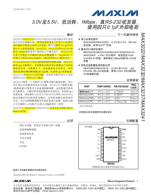
MAX3222/MAX3232/MAX3237/MAX32413.0V至5.5V、低功耗、1Mbps、真RS-232收发器,使用四只0.1µF外部电容________________________________________________________________Maxim Integrated Products119-0273; Rev 7; 1/07MegaBaud和UCSP是Maxim Integrated Products, Inc.的商标。
本文是英文数据资料的译文,文中可能存在翻译上的不准确或错误。
如需进一步确认,请在您的设计中参考英文资料。
有关价格、供货及订购信息,请联络Maxim亚洲销售中心:10800 852 1249 (北中国区),10800 152 1249 (南中国区),或访问Maxim的中文网站:。
M A X 3222/M A X 3232/M A X 3237/M A X 32413.0V至5.5V、低功耗、1Mbps、真RS-232收发器,使用四只0.1µF外部电容2_______________________________________________________________________________________ABSOLUTE MAXIMUM RATINGSELECTRICAL CHARACTERISTICS(V CC = +3.0V to +5.5V, C1–C4 = 0.1µF (Note 2), T A = T MIN to T MAX , unless otherwise noted. Typical values are at T A = +25°C.)Stresses beyond those listed under “Absolute Maximum Ratings” may cause permanent damage to the device. These are stress ratings only, and functional operation of the device at these or any other conditions beyond those indicated in the operational sections of the specifications is not implied. Exposure to absolute maximum rating conditions for extended periods may affect device reliability.Note 1:V+ and V- can have a maximum magnitude of 7V, but their absolute difference cannot exceed 13V.V CC ...........................................................................-0.3V to +6V V+ (Note 1)...............................................................-0.3V to +7V V- (Note 1)................................................................+0.3V to -7V V+ + V- (Note 1)...................................................................+13V Input VoltagesT_IN, SHDN , EN ...................................................-0.3V to +6V MBAUD...................................................-0.3V to (V CC + 0.3V)R_IN.................................................................................±25V Output VoltagesT_OUT...........................................................................±13.2V R_OUT....................................................-0.3V to (V CC + 0.3V)Short-Circuit DurationT_OUT....................................................................ContinuousContinuous Power Dissipation (T A = +70°C)16-Pin TSSOP (derate 6.7mW/°C above +70°C).............533mW 16-Pin Narrow SO (derate 8.70mW/°C above +70°C)....696mW 16-Pin Wide SO (derate 9.52mW/°C above +70°C)........762mW 16-Pin Plastic DIP (derate 10.53mW/°C above +70°C)...842mW 18-Pin SO (derate 9.52mW/°C above +70°C)..............762mW 18-Pin Plastic DIP (derate 11.11mW/°C above +70°C)..889mW 20-Pin SSOP (derate 7.00mW/°C above +70°C).........559mW 20-Pin TSSOP (derate 8.0mW/°C above +70°C).............640mW 28-Pin TSSOP (derate 8.7mW/°C above +70°C).............696mW 28-Pin SSOP (derate 9.52mW/°C above +70°C).........762mW 28-Pin SO (derate 12.50mW/°C above +70°C).....................1W Operating Temperature RangesMAX32_ _C_ _.....................................................0°C to +70°C MAX32_ _E_ _ .................................................-40°C to +85°C Storage Temperature Range.............................-65°C to +150°C Lead Temperature (soldering, 10s).................................+300°CMAX3222/MAX3232/MAX3237/MAX32413.0V至5.5V、低功耗、1Mbps、真RS-232收发器,使用四只0.1µF外部电容_______________________________________________________________________________________3TIMING CHARACTERISTICS—MAX3222/MAX3232/MAX3241(V CC = +3.0V to +5.5V, C1–C4 = 0.1µF (Note 2), T A = T MIN to T MAX , unless otherwise noted. Typical values are at T A = +25°C.)ELECTRICAL CHARACTERISTICS (continued)(V CC = +3.0V to +5.5V, C1–C4 = 0.1µF (Note 2), T A = T MIN to T MAX , unless otherwise noted. Typical values are at T A = +25°C.)A X 3222/M A X 3232/M A X 3237/M A X 32413.0V至5.5V、低功耗、1Mbps、真RS-232收发器,使用四只0.1µF外部电容4_______________________________________________________________________________________典型工作特性Ω, T A = +25°C, unless otherwise noted.)LOAD CAPACITANCE (pF)0246810121416182022150MAX3222/MAX3232SLEW RATEvs. LOAD CAPACITANCELOAD CAPACITANCE (pF)S L E W R A T E (V /µs )20003000100040005000510152025303540MAX3222/MAX3232SUPPLY CURRENT vs. LOAD CAPACITANCEWHEN TRANSMITTING DATALOAD CAPACITANCE (pF)S U P P L Y C U R R E N T (m A )20003000100040005000TIMING CHARACTERISTICS—MAX3237(V CC = +3.0V to +5.5V, C1–C4 = 0.1µF (Note 2), T A = T MIN to T MAX , unless otherwise noted. Typical values are at T A = +25°C.)Note 2:MAX3222/MAX3232/MAX3241: C1–C4 = 0.1µF tested at 3.3V ±10%; C1 = 0.047µF, C2–C4 = 0.33µF tested at 5.0V ±10%.MAX3237: C1–C4 = 0.1µF tested at 3.3V ±5%; C1–C4 = 0.22µF tested at 3.3V ±10%; C1 = 0.047µF, C2–C4 = 0.33µF tested at 5.0V ±10%.Note 3:Transmitter input hysteresis is typically 250mV.MAX3222/MAX3232/MAX3237/MAX32413.0V至5.5V、低功耗、1Mbps、真RS-232收发器,使用四只0.1µF外部电容_______________________________________________________________________________________5-7.5-5.0-2.502.55.07.50MAX3241TRANSMITTER OUTPUT VOLTAGEvs. LOAD CAPACITANCELOAD CAPACITANCE (pF)T R A N S M I T T E R O U T P U T V O L T A G E (V )2000300010004000500046810121416182022240MAX3241SLEW RATEvs. LOAD CAPACITANCELOAD CAPACITANCE (pF)S L E W R A T E (V /µs )20003000100040005000510152025303545400MAX3241SUPPLY CURRENT vs. LOADCAPACITANCE WHEN TRANSMITTING DATALOAD CAPACITANCE (pF)S U P P L Y C U R R E N T (m A )20003000100040005000-7.5-5.0-2.502.55.07.50MAX3237TRANSMITTER OUTPUT VOLTAGE vs. LOAD CAPACITANCE (MBAUD = GND)LOAD CAPACITANCE (pF)T R A N S M I T T E R O U T P U T V O L T A G E (V )200030001000400050000102030504060700MAX3237SLEW RATE vs. LOAD CAPACITANCE(MBAUD = V CC )LOAD CAPACITANCE (pF)S L E W R A T E (V /µs )500100015002000-7.5-5.0-2.502.55.07.50MAX3237TRANSMITTER OUTPUT VOLTAGE vs. LOAD CAPACITANCE (MBAUD = V CC )LOAD CAPACITANCE (pF)T R A N S M I T T E R O U T P U T V O L T A G E (V )5001000150020001020304050600MAX3237SUPPLY CURRENT vs.LOAD CAPACITANCE (MBAUD = GND)LOAD CAPACITANCE (pF)S U P P L Y C U R R E N T (m A )200030001000400050000246810120MAX3237SLEW RATE vs. LOAD CAPACITANCE(MBAUD = GND)LOAD CAPACITANCE (pF)S L E W R A T E (V /µs )2000300010004000500010302040506070MAX3237SKEW vs. LOAD CAPACITANCE(t PLH - t PHL )LOAD CAPACITANCE (pF)1000150050020002500____________________________________________________________________典型工作特性(续)(V CC = +3.3V, 235kbps data rate, 0.1µF capacitors, all transmitters loaded with 3k Ω, T A = +25°C, unless otherwise noted.)M A X 3222/M A X 3232/M A X 3237/M A X 32413.0V至5.5V、低功耗、1Mbps、真RS-232收发器,使用四只0.1µF外部电容6_________________________________________________________________________________________________________________________________________________________________引脚说明MAX3222/MAX3232/MAX3237/MAX32413.0V至5.5V、低功耗、1Mbps、真RS-232收发器,使用四只0.1µF外部电容_______________________________________________________________________________________7_______________________________详细说明双电荷泵电压转换器MAX3222/MAX3232/MAX3237/MAX3241的内部电源由两路稳压型电荷泵组成,只要输入电压(V CC )在3.0V至5.5V范围以内,即可提供+5.5V (倍压电荷泵)和-5.5V (反相电荷泵)输出电压。
MAX6373KA+T中文资料

General DescriptionThe MAX6369–MAX6374 are pin-selectable watchdog timers that supervise microprocessor (µP) activity and signal when a system is operating improperly. During normal operation, the microprocessor should repeated-ly toggle the watchdog input (WDI) before the selected watchdog timeout period elapses to demonstrate that the system is processing code properly. If the µP does not provide a valid watchdog input transition before the timeout period expires, the supervisor asserts a watch-dog (WDO ) output to signal that the system is not exe-cuting the desired instructions within the expected time frame. The watchdog output pulse can be used to reset the µP or interrupt the system to warn of processing errors.The MAX6369–MAX6374 are flexible watchdog timer supervisors that can increase system reliability through notification of code execution errors. The family offers several pin-selectable watchdog timing options to match a wide range of system timing applications:•Watchdog startup delay: provides an initial delay before the watchdog timer is started.•Watchdog timeout period: normal operating watch-dog timeout period after the initial startup delay.•Watchdog output/timing options: open drain (100ms)or push-pull (1ms).The MAX6369–MAX6374 operate over a +2.5V to +5.5V supply range and are available in miniature 8-pin SOT23 packages.________________________ApplicationsEmbedded Control Systems Industrial ControllersCritical µP and Microcontroller (µC) Monitoring AutomotiveTelecommunications NetworkingFeatures♦Precision Watchdog Timer for Critical µP Applications ♦Pin-Selectable Watchdog Timeout Periods ♦Pin-Selectable Watchdog Startup Delay Periods ♦Ability to Change Watchdog Timing Characteristics Without Power Cycling ♦Open-Drain or Push-Pull Pulsed Active-Low Watchdog Output ♦Watchdog Timer Disable Feature ♦+2.5V to +5.5V Operating Voltage ♦8µA Low Supply Current♦No External Components Required ♦Miniature 8-Pin SOT23 PackageMAX6369–MAX6374Pin-Selectable Watchdog Timers19-1676; Rev 3; 11/05Ordering InformationPin Configuration appears at end of data sheet.Note:All devices are available in tape-and-reel only. Required order increment is 2,500 pieces.Devices are available in both leaded and lead-free packaging.Specify lead-free by replacing “-T” with “+T” when ordering.Selector GuideFor pricing, delivery, and ordering information,please contact Maxim/Dallas Direct!at1-888-629-4642, or visit Maxim’s website at .M A X 6369–M A X 6374Pin-Selectable Watchdog Timers 2_______________________________________________________________________________________ABSOLUTE MAXIMUM RATINGSELECTRICAL CHARACTERISTICS(V CC = +2.5V to +5.5V, SET_ = V CC or GND, T A = -40°C to +85°C, unless otherwise noted. Typical values are at T A = +25°C andStresses beyond those listed under “Absolute Maximum Ratings” may cause permanent damage to the device. These are stress ratings only, and functional operation of the device at these or any other conditions beyond those indicated in the operational sections of the specifications is not implied. Exposure to absolute maximum rating conditions for extended periods may affect device reliability.Terminal Voltage (with respect to GND)V CC .....................................................................-0.3V to +6V WDI.....................................................................-0.3V to +6V WDO (Open Drain: MAX6369/71/73).................-0.3V to +6V WDO (Push-Pull: MAX6370/72/74 .......-0.3V to (V CC + 0.3V)SET0, SET1, SET2................................-0.3V to (V CC + 0.3V)Maximum Current, Any Pin (input/output)...........................20mAContinuous Power Dissipation (T A = +70°C)SOT23-8 (derate 8.75mW/°C above +70°C)...............700mW Operating Temperature Range ...........................-40°C to +85°C Storage Temperature Range.............................-65°C to +150°C Junction Temperature......................................................+150°C Lead Temperature (soldering, 10s).................................+300°C V CC Rise or Fall Rate......................................................0.05V/µsMAX6369–MAX6374Pin-Selectable Watchdog Timers_______________________________________________________________________________________3ELECTRICAL CHARACTERISTICS (continued)M A X 6369–M A X 6374Pin-Selectable Watchdog Timers 4_______________________________________________________________________________________461081214-4010-15356085SUPPLY CURRENT vs. TEMPERATURETEMPERATURE (°C)S U P P L Y C U R R E N T (µA )Typical Operating Characteristics(Circuit of Figure 1, T A = +25°C, unless otherwise noted .)0.9970.9990.9981.0011.0001.0021.003-4010-15356085WATCHDOG TIMEOUT PERIODvs. TEMPERATUREM A X 6369/74-02TEMPERATURE (°C)N O R M A L I Z E D W A T C H D O G T I M E O U T P E R I O DELECTRICAL CHARACTERISTICS (continued)Note 2:Guaranteed by design.Note 3:In this setting the watchdog timer is inactive and startup delay ends when WDI sees its first level transition. See SelectingDevice Timing for more information.Note 4:After power-up, or a setting change, there is an internal setup time during which WDI is ignored.MAX6369–MAX6374Pin-Selectable Watchdog Timers_______________________________________________________________________________________5Pin DescriptionDetailed DescriptionThe MAX6369–MAX6374 are flexible watchdog circuits for monitoring µP activity. During normal operation, the internal timer is cleared each time the µP toggles the WDI with a valid logic transition (low to high or high to low) within the selected timeout period (t WD ). The WDO remains high as long as the input is strobed within the selected timeout period. If the input is not strobed before the timeout period expires, the watchdog output is asserted low for the watchdog output pulse width (t WDO ). The device type and the state of the three logic control pins (SET0, SET1, and SET2) determine watch-dog timing characteristics. The three basic timing varia-tions for the watchdog startup delay and the normalTable 1 for the timeout characteristics for all devices in the family):•Watchdog Startup Delay:Provides an initial delay before the watchdog timer is started.Allows time for the µP system to power up and initial-ize before assuming responsibility for normal watch-dog timer updates.Includes several fixed or pin-selectable startup delay options from 200µs to 60s, and an option to wait for the first watchdog input transition before starting the watchdog timer.M A X 6369–M A X 6374Pin-Selectable Watchdog Timers 6_______________________________________________________________________________________•Watchdog Timeout Period:Normal operating watchdog timeout period after the initial startup delay.A watchdog output pulse is asserted if a valid watch-dog input transition is not received before the timeout period elapses.Eight pin-selectable timeout period options for each device, from 30µs to 60s.Pin-selectable watchdog timer disable feature.•Watchdog Output/Timing Options:Open drain, active low with 100ms minimum watch-dog output pulse (MAX6369/MAX6371/MAX6373).Push-pull, active low with 1ms minimum watchdog output pulse (MAX6370/MAX6372/MAX6374).Each device has a watchdog startup delay that is initi-ated when the supervisor is first powered or after the user modifies any of the logic control set inputs. The watchdog timer does not begin to count down until theFigure 1. Functional Diagramcompletion of the startup delay period, and no watch-dog output pulses are asserted during the startup delay. When the startup delay expires, the watchdog begins counting its normal watchdog timeout period and waiting for WDI transitions. The startup delay allows time for the µP system to power up and fully ini-tialize before assuming responsibility for the normal watchdog timer updates. Startup delay periods vary between the different devices and may be altered by the logic control set pins. To ensure that the system generates no undesired watchdog outputs, the routine watchdog input transitions should begin before the selected minimum startup delay period has expired. The normal watchdog timeout period countdown is initi-ated when the startup delay is complete. If a valid logic transition is not recognized at WDI before the watchdog timeout period has expired, the supervisor asserts a watchdog output. Watchdog timeout periods vary between the different devices and may be altered by the logic control set pins. To ensure that the system generates no undesired watchdog outputs, the watch-dog input transitions should occur before the selected minimum watchdog timeout period has expired.The startup delay and the watchdog timeout period are determined by the states of the SET0, SET1, and SET2 pins, and by the particular device within the family. For the MAX6369 and MAX6370, the startup delay is equal to the watchdog timeout period. The startup and watchdog timeout periods are pin selectable from 1ms to 60s (minimum).For the MAX6371 and MAX6372, the startup delay is fixed at 60s and the watchdog timeout period is pin selectable from 1ms to 60s (minimum).The MAX6373/MAX6374 provide two timing variations for the startup delay and normal watchdog timeout. Five of the pin-selectable modes provide startup delays from 200µs to 60s minimum, and watchdog timeout delays from 3ms to 10s minimum. Two of the selectable modes do not initiate the watchdog timer until the device receives its first valid watchdog input transition (there is no fixed period by which the first input must be received). These two extended startup delay modesare useful for applications requiring more than 60s for system initialization.All the MAX6369–MAX6374 devices may be disabledwith the proper logic control pin setting (Table 1).Applications InformationInput Signal Considerations Watchdog timing is measured from the last WDI risingor falling edge associated with a pulse of at least 100nsin width. WDI transitions are ignored when WDO is asserted, and during the startup delay period (Figure2). Watchdog input transitions are also ignored for asetup period, t SETUP, of up to 300µs after power-up ora setting change (Figure 3).Selecting Device TimingSET2, SET1, and SET0 program the startup delay and watchdog timeout periods (Table 1). Timeout settingscan be hard wired, or they can be controlled with logicgates and modified during operation. To ensure smooth transitions, the system should strobe WDI immediately before the timing settings are changed. This minimizesthe risk of initializing a setting change too late in thetimer countdown period and generating undesired watchdog outputs. After changing the timing settings,two outcomes are possible based on WDO. If the change is made while WDO is asserted, the previous setting is allowed to finish, the characteristics of thenew setting are assumed, and the new startup phase is entered after a 300µs setup time (t SETUP) elapses. Ifthe change is made while WDO is not asserted, thenew setting is initiated immediately, and the new start-up phase is entered after the 300µs setup time elapses.MAX6369–MAX6374Pin-Selectable Watchdog Timers_______________________________________________________________________________________7 Figure 3. Setting Change TimingM A X 6369–M A X 6374Pin-Selectable Watchdog TimersSelecting 011 (SET2 = 0, SET1 = 1, SET0 = 1) disables the watchdog timer function on all devices in the family.Operation can be reenabled without powering down by changing the set inputs to the new desired setting. The device assumes the new selected timing characteris-tics and enter the startup phase after the 300µs setup time elapses (Figure 3).The MAX6373/MAX6374 offer a first-edge feature. In first-edge mode (settings 101 or 110, Table 1), the internal timer does not control the startup delay period.Instead, startup terminates when WDI sees a transition.If changing to first-edge mode while the device is oper-ating, disable mode must be entered first. It is then safe to select first-edge mode. Entering disable mode first ensures the output is unasserted when selecting first-edge mode and removes the danger of WDI being masked out.OutputThe MAX6369/MAX6371/MAX6373 have an active-low,open-drain output that provides a watchdog output pulse of 100ms. This output structure sinks current when WDO is asserted. Connect a pullup resistor from WDO to any supply voltage up to +5.5V.Select a resistor value large enough to register a logic low (see Ele ctrical Characte ristics ), and small enoughto register a logic high while supplying all input current and leakage paths connected to the WDO line. A 10k Ωpullup is sufficient in most applications. The MAX6370/MAX6372/MAX6374 have push-pull outputs that pro-vide an active-low watchdog output pulse of 1ms.When WDO deasserts, timing begins again at the beginning of the watchdog timeout period (Figure 2).Usage in Noisy EnvironmentsIf using the watchdog timer in an electrically noisy envi-ronment, a bypass capacitor of 0.1µF should be con-nected between V CC and GND as close to the device as possible, and no further away than 0.2 inches.________________Watchdog SoftwareConsiderationsTo help the watchdog timer monitor software execution more closely, set and reset the watchdog input at differ-ent points in the program, rather than pulsing the watch-dog input high-low-high or low-high-low. This technique avoids a stuck loop, in which the watchdog timer would continue to be reset inside the loop, keeping the watch-dog from timing out. Figure 4 shows an example of a flow diagram where the I/O driving the watchdog input is set high at the beginning of the program, set low at the end of every subroutine or loop, then set high again when the program returns to the beginning. If the pro-gram should hang in any subroutine, the problem would be quickly corrected, since the I/O is continually set low and the watchdog timer is allowed to time out, causing WDO to pulse.Figure 4. Watchdog Flow DiagramChip InformationTRANSISTOR COUNT: 1500PROCESS: BiCMOSPin ConfigurationMaxim cannot assume re sponsibility for use of any circuitry othe r than circuitry e ntire ly e mbodie d in a Maxim product. No circuit pate nt lice nse s are implied. Maxim reserves the right to change the circuitry and specifications without notice at any time.8_____________________Maxim Integrated Products, 120 San Gabriel Drive, Sunnyvale, CA 94086 408-737-7600©2005 Maxim Integrated ProductsPrinted USAis a registered trademark of Maxim Integrated Products, Inc.。
MAX832CWE中文资料
STEP-DOWN CONVER________________________________________________________________ Maxim Integrated Products
1
Call toll free 1-800-998-8800 for free samples or literature.
元器件交易网
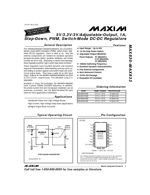
5V/3.3V/3V/Adjustable-Output, 1A, Step-Down, PWM, Switch-Mode DC-DC Regulators MAX830–MAX833
ABSOLUTE MAXIMUM RATINGS
Input Voltage . . . . . . . . . . . . . . . . . . . . . . . . . . . . . . . . . . . . . . . . . . . . . . . . . . 40V Switch Voltage with Respect to Input Voltage. . . . . . . . . . . . . . . . 50V Switch Voltage with Respect to GND (VSW negative) (Note 1). . . . . . . . . . . . . . . . . . . . . . . . . . . . . . . . . . . . . 20V FB/SENSE Voltage . . . . . . . . . . . . . . . . . . . . . . . . . . . . . . . . . . . -0.3V, +10V SHUT Voltage (not to exceed VIN) . . . . . . . . . . . . . . . . . . . . . . . . . . . . 30V Note 1: Do not exceed switch-to-input voltage limitation.
MEMORY存储芯片MAX823TEUK+T中文规格书
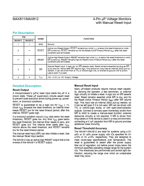
Manual Reset Input Many μP-based products require manual reset capabil -ity, allowing the operator, a test technician, or external logic circuitry to initiate a reset. A logic low on MR asserts reset. Reset remains asserted while MR is low, and for the Reset Active Timeout Period (t RP ) after MR returns high. This input has an internal 20kΩ pull-up resistor, so it can be left open if it is not used. MR can be driven with TTL or CMOS-logic levels, or with open-drain/collector outputs. Connect a normally open momentary switch from MR to GND to create a manual-reset function; external debounce circuitry is not required. If MR is driven from long cables or if the device is used in a noisy environment, connecting a 0.1μF capacitor from MR to ground provides additional noise immunity.Reset Threshold Accuracy The MAX811/MAX812 are ideal for systems using a 5V ±5% or 3V ±5% power supply with ICs specified for 5V ±10% or 3V ±10%, respectively. They are designed to meet worst-case specifications over temperature. The reset is guaranteed to assert after the power supplyfalls out of regulation, but before power drops below theminimum specified operating voltage range for the systemICs. The thresholds are pre-trimmed and exhibit tight dis -tribution, reducing the range over which an undesirable reset may occur.PINNAME FUNCTION MAX811MAX81211GND Ground 2—RESET Active-Low Reset Output. RESET remains low while V CC is below the reset threshold or while MR is held low. RESET remains low for the Reset Active Timeout Period (t RP ) after the reset conditions are terminated.—2RESET Active-High Reset Output. RESET remains high while V CC is below the reset threshold or while MR is held low. RESET remains high for Reset Active Timeout Period (t RP ) after the reset conditions are terminated.33MR Manual Reset Input. A logic low on MR asserts reset. Reset remains asserted as long as MR is low and for 180ms after MR returns high. This active-low input has an internal 20kΩ pull-up resistor. It can be driven from a TTL or CMOS-logic line, or shorted to ground with a switch. Leave open if unused.44V CC +5V, +3.3V, or +3V Supply Voltage Detailed DescriptionReset OutputA microprocessor’s (μP’s) reset input starts the μP in aknown state. These μP supervisory circuits assert resetto prevent code execution errors during power-up, power-down, or brownout conditions.RESET is guaranteed to be a logic low for V CC > 1V.Once V CC exceeds the reset threshold, an internal timerkeeps RESET low for the reset timeout period; after thisinterval, RESET goes high.If a brownout condition occurs (V CC dips below the resetthreshold), RESET goes low. Any time V CC goes belowthe reset threshold, the internal timer resets to zero, andRESET goes low. The internal timer starts after V CC returns above the reset threshold, and RESET remainslow for the reset timeout period.The manual reset input (MR ) can also initiate a reset. See the Manual Reset Input section.The MAX812 has an active-high RESET output that is theinverse of the MAX811’s RESET output.MAX811/MAX8124-Pin μP Voltage Monitorswith Manual Reset InputPin DescriptionTerminal Voltage (with respect to GND)V CC.....................................................................-0.3V to 6.0V All Other Inputs .....................................-0.3V to (V CC + 0.3V) Input Current, V CC, MR......................................................20mA Output Current, RESET or RESET ....................................20mA Continuous Power Dissipation (T A = +70°C)SOT143 (derate 4mW/°C above +70°C) .....................320mW Operating Temperature Range ...........................-40°C to +85°C Junction Temperature ......................................................+150°C Storage Temperature Range ............................-65°C to +160°C Lead Temperature (soldering, 10sec) .............................+300°C(V CC = 5V for L/M versions, V CC = 3.3V for T/S versions, V CC = 3V for R version, T A = -40°C to +85°C, unless otherwise noted. Typical values are at T A = +25°C.) (Note 1)PARAMETER SYMBOL CONDITIONS MIN TYP MAX UNITSOperating Voltage Range V CC T A = 0°C to +70°C 1.0 5.5V T A = -40°C to +85°C 1.2Supply Current I CC MAX81_L/M, V CC = 5.5V, I OUT = 0615µA MAX81_R/S/T, V CC = 3.6V, I OUT = 0 2.710Reset Threshold V TH MAX81_LT A = +25°C 4.54 4.63 4.72V T A = -40°C to +85°C 4.50 4.75MAX81_MT A = +25°C 4.30 4.38 4.46T A = -40°C to +85°C 4.25 4.50MAX81_TT A = +25°C 3.03 3.08 3.14T A = -40°C to +85°C 3.00 3.15MAX81_ST A = +25°C 2.88 2.93 2.98T A = -40°C to +85°C 2.85 3.00MAX81_RT A = +25°C 2.58 2.63 2.68T A = -40°C to +85°C 2.55 2.70Reset Threshold Tempco30ppm/°CV CC to Reset Delay (Note 2)V OD = 125mV, MAX81_L/M40µs V OD = 125mV, MAX81_R/S/T20Reset Active Timeout Period t RP V CC = V TH(MAX)140560ms MR Minimum Pulse Width t MR10µs MR Glitch Immunity (Note 3)100ns MR to Reset PropagationDelay (Note 2)t MD0.5µsMR Input Threshold V IHV CC > V TH(MAX), MAX81_L/M2.3V V IL0.8V IHV CC > V TH(MAX), MAX81_R/S/T0.7 x V CCV IL0.25 x V CCMR Pull-Up Resistance102030kΩRESET Output Voltage (MAX812)V OH I SOURCE = 150µA, 1.8V < V CC < V TH(MIN)0.8 x V CCV V OLMAX812R/S/T only, I SINK = 1.2mA,V CC = V TH(MAX)0.3MAX812L/M only, I SINK = 3.2mA,V CC = V TH(MAX)0.4MAX811/MAX8124-Pin μP Voltage Monitorswith Manual Reset Input Absolute Maximum RatingsStresses beyond those listed under “Absolute Maximum Ratings” may cause permanent damage to the device. These are stress ratings only, and functional operation of the device at these or any other conditions beyond those indicated in the operational sections of the specifications is not implied. Exposure to absolute maximum rating conditions for extended periods may affect device reliability.Electrical Characteristics。
- 1、下载文档前请自行甄别文档内容的完整性,平台不提供额外的编辑、内容补充、找答案等附加服务。
- 2、"仅部分预览"的文档,不可在线预览部分如存在完整性等问题,可反馈申请退款(可完整预览的文档不适用该条件!)。
- 3、如文档侵犯您的权益,请联系客服反馈,我们会尽快为您处理(人工客服工作时间:9:00-18:30)。
General Description The MAX6381–MAX6390 microprocessor (µP) supervisory circuits monitor power-supply voltages from +1.8V to +5.0V while consuming only 3µA of supply current at +1.8V. Whenever V CC falls below the factory-set reset thresholds, the reset output asserts and remains assert-ed for a minimum reset timeout period after V CC rises above the reset threshold. Reset thresholds are available from +1.58V to +4.63V, in approximately 100mV incre-ments. Seven minimum reset timeout delays ranging from 1ms to 1200ms are available.The MAX6381/MAX6384/MAX6387 have a push-pull active-low reset output. The MAX6382/MAX6385/ MAX6388 have a push-pull active-high reset output, and the MAX6383/MAX6386/MAX6389/MAX6390 have an open-drain active-low reset output. The MAX6384/MAX6385/MAX6386 also feature a debounced manual reset input (with internal pullup resistor). The MAX6387/MAX6388/MAX6389 have an auxiliary input for monitoring a second voltage. The MAX6390 offers a manual reset input with a longer V CC reset timeout period (1120ms or 1200ms) and a shorter manual reset timeout (140ms or 150ms).The MAX6381/MAX6382/MAX6383 are available in 3-pin SC70 and6-pinµDFN packages and the MAX6384–MAX6390 are available in 4-pin SC70 andFeatures♦Factory-Set Reset Threshold Voltages Rangingfrom +1.58V to +4.63V in Approximately 100mVIncrements♦±2.5% Reset Threshold Accuracy OverTemperature (-40°C to +125°C)♦Seven Reset Timeout Periods Available: 1ms,20ms, 140ms, 280ms, 560ms, 1120ms,1200ms (min)♦3 Reset Output OptionsActive-Low Push-PullActive-High Push-PullActive-Low Open-Drain♦Reset Output State Guaranteed ValidDown to V CC= 1V♦Manual Reset Input (MAX6384/MAX6385/MAX6386)♦Auxiliary RESET IN(MAX6387/MAX6388/MAX6389)♦V CC Reset Timeout (1120ms or 1200ms)/ManualReset Timeout (140ms or 150ms) (MAX6390)♦Negative-Going V CC Transient Immunity♦Low Power Consumption of 6µA at +3.6Vand 3µA at +1.8V♦Pin Compatible withMAX809/MAX810/MAX803/MAX6326/MAX6327/MAX6328/MAX6346/MAX6347/MAX6348,and MAX6711/MAX6712/MAX6713♦Tiny 3-Pin/4-Pin SC70 and 6-Pin µDFN PackagesMAX6381–MAX6390 SC70/µDFN, Single/Dual Low-Voltage,Low-Power µP Reset Circuits ________________________________________________________________Maxim Integrated Products1Pin Configurations19-1839; Rev 4; 4/07Ordering InformationOrdering Information continued at end of data sheet.Typi cal Operati ng Ci rcui t appears at end of data sheet.Selector Guide appears at end of data sheet.after "XR", "XS", or "LT." Insert reset timeout delay (see ResetTimeout Delay table) after "D" to complete the part number.Sample stock is generally held on standard versions only (seeStandard Versions table). Standard versions have an orderincrement requirement of 2500 pieces. Nonstandard versionshave an order increment requirement of 10,000 pieces.Contact factory for availability of nonstandard versions.+Denotes a lead-free package.For pricing, delivery, and ordering information,please contact Maxim Direct at 1-888-629-4642,or visit Maxim’s website at .ComputersControllersIntelligent InstrumentsCritical µP and µCPower MonitoringPortable/Battery-Powered EquipmentDual Voltage SystemsM A X 6381–M A X 6390SC70/µDFN, Single/Dual Low-Voltage, Low-Power µP Reset CircuitsABSOLUTE MAXIMUM RATINGSELECTRICAL CHARACTERISTICS(V CC = full range, T A = -40°C to +125°C, unless otherwise specified. Typical values are at T A = +25°C.) (Note 1)Stresses beyond those listed under “Absolute Maximum Ratings” may cause permanent damage to the device. These are stress ratings only, and functional operation of the device at these or any other conditions beyond those indicated in the operational sections of the specifications is not implied. Exposure to absolute maximum rating conditions for extended periods may affect device reliability.V CC to GND..........................................................-0.3V to +6.0V RESET Open-Drain Output....................................-0.3V to +6.0V RESET , RESET (push-pull output)..............-0.3V to (V CC + 0.3V)MR , RESET IN.............................................-0.3V to (V CC + 0.3V)Input Current (V CC ).............................................................20mA Output Current (all pins).....................................................20mAContinuous Power Dissipation (T A = +70°C)3-Pin SC70 (derate 2.9mW/°C above +70°C)..............235mW 4-Pin SC70 (derate 3.1mW/°C above +70°C)..............245mW 6-Pin µDFN (derate 2.1mW/°C above +70°C)..........167.7mW Operating Temperature Range .........................-40°C to +125°C Storage Temperature Range.............................-65°C to +150°C Lead Temperature (soldering, 10s).................................+300°CMAX6381–MAX6390SC70/µDFN, Single/Dual Low-Voltage,Low-Power µP Reset Circuits_______________________________________________________________________________________3M A X 6381–M A X 6390SC70/µDFN, Single/Dual Low-Voltage, Low-Power µP Reset Circuits 4______________________________________________________________________________________Typical Operating Characteristics(T A = +25°C, unless otherwise noted.)215436789-40-105-25203550658095110125SUPPLY CURRENT vs. TEMPERATURE(NO LOAD)TEMPERATURE (°C)S U P P L Y C U R R E N T (µA )25292735333137394143-40-105-25203550658095110125POWER-DOWN RESET DELAYvs. TEMPERATURETEMPERATURE (°C)P O W E R -D O W N R E S E T D E L A Y (µs )0.940.980.961.021.001.061.041.08-40-10520-253550658095110125NORMALIZED POWER-UP RESET TIMEOUTvs. TEMPERATUREM A X 6381/90 t o c 03TEMPERATURE (°C)N O R M A L I Z E D R E S E T T I M E O U T P E R I O D0.9900.9851.0150.9950.9901.0001.0051.0101.020-40-10520-253550958011065125M A X 6381/90 t o c 04TEMPERATURE (°C)N O R M A L I Z E D R E S E T TH R E S H O L D NORMALIZED RESET THRESHOLDvs. TEMPERATURE00.40.20.80.61.01.2063912OUTPUT-VOLTAGE LOW vs. SINK CURRENTI SINK (mA)V O L (V )01.00.52.01.52.53.00500750250100012501500OUTPUT-VOLTAGE HIGH vs. SOURCE CURRENTI SOURCE (µA)V O H (V )45001100010010MAXIMUM TRANSIENT DURATION vs. RESET COMPARATOR OVERDRIVE15050350250500200100400300RESET COMPARATOR OVERDRIVE, V TH - V CC (mV)M A X I M U M T R A N S I E N T D U R A T I O N (µs )3.53.93.74.54.34.14.74.95.35.15.5-40-105-25203550658095110125RESET IN TO RESET DELAYvs. TEMPERATUREM A X 6381/90 t o c 08TEMPERATURE (°C)R E S E T I N D E L A Y (µs )MAX6381–MAX6390SC70/µDFN, Single/Dual Low-Voltage,Low-Power µP Reset CircuitsPin DescriptionM A X 6381–M A X 6390SC70/µDFN, Single/Dual Low-Voltage, Low-Power µP Reset Circuits 6_______________________________________________________________________________________Detailed DescriptionRESET OutputA µP reset input starts the µP in a known state. These µP supervisory circuits assert reset to prevent code execution errors during power-up, power-down, or brownout conditions.Reset asserts when V CC is below the reset threshold;once V CC exceeds the reset threshold, an internal timer keeps the reset output asserted for the reset timeout period. After this interval, reset output deasserts. Reset output is guaranteed to be in the correct logic state for V CC ≥1V.Manual Reset Input (MAX6384/MAX6385/MAX6386/MAX6390)Many µP-based products require manual reset capabil-ity, allowing the operator, a test technician, or external logic circuitry to initiate a reset. A logic low on MR asserts reset. Reset remains asserted while MR is low,and for the reset active timeout period (t RP ) after MR returns high. This input has an internal 63k Ωpullup resistor (1.56k Ωfor MAX6390), so it can be left uncon-nected if it is not used. MR can be driven with TTL or CMOS logic levels, or with open-drain/collector outputs.Connect a normally open momentary switch from MR to G ND to create a manual-reset function; external debounce circuitry is not required. If MR is driven from long cables or if the device is used in a noisy environ-ment, connecting a 0.1µF capacitor from MR to G ND provides additional noise immunity.RESET IN Comparator(MAX6387/MAX6388/MAX6389)RESET IN is compared to an internal +1.27V reference.If the voltage at RESET IN is less than 1.27V, reset asserts. Use the RESET IN comparator as a user-adjustable reset detector or as a secondary power-sup-ply monitor by implementing a resistor-divider at RESET IN (shown in Figure 1). Reset asserts when either V CC or RESET IN falls below its respective threshold volt-age. Use the following equation to set the threshold:V INTH = V THRST (R1/R2 + 1)where V THRST = +1.27V. To simplify the resistor selec-tion, choose a value of R2 and calculate R1:R1 = R2 [(V INTH /V THRST ) - 1]Since the input current at RESET IN is 50nA (max),large values can be used for R2 with no significant loss in accuracy.___________Applications InformationNegative-Going V CC TransientsIn addition to issuing a reset to the µP during power-up,power-down, and brownout conditions, the MAX6381–MAX6390 are relatively immune to short dura-tion negative-going V CC transients (glitches).The Typical Operating Characteristics section shows the Maximum Transient Durations vs. Reset Comparator Overdrive, for which the MAX6381–MAX6390 do not generate a reset pulse. This graph was generated usinga negative-going pulse applied to V CC , starting above the actual reset threshold and ending below it by the magnitude indicated (reset comparator overdrive). The graph indicates the typical maximum pulse width a neg-ative-going V CC transient may have without causing a reset pulse to be issued. As the magnitude of the tran-sient increases (goes farther below the reset threshold),the maximum allowable pulse width decreases. A 0.1µF capacitor mounted as close as possible to V CC provides additional transient immunity.Ensuring a Valid RESET Output Down to V CC = 0VThe MAX6381–MAX6390 are guaranteed to operate properly down to V CC = 1V. In applications that require valid reset levels down to V CC = 0V, a pulldown resistor to active-low outputs (push/pull only, Figure 2) and a pullup resistor to active-high outputs (push/pull only)will ensure that the reset line is valid while the reset out-put can no longer sink or source current. This schemedoes not work with the open-drain outputs of the MAX6383/MAX6386/MAX6389/MAX6390. The resistor value used is not critical, but it must be small enough not to load the reset output when V CC is above the reset threshold. For most applications, 100k Ωis ade-quate.MAX6381–MAX6390SC70/µDFN, Single/Dual Low-Voltage,Low-Power µP Reset Circuits_______________________________________________________________________________________7M A X 6381–M A X 6390SC70/µDFN, Single/Dual Low-Voltage, Low-Power µP Reset Circuits 8_______________________________________________________________________________________Selector GuideOrdering Information (continued)Note:Insert reset threshold suffix (see Reset Threshold table)after "XR", "XS", or "LT." Insert reset timeout delay (see Reset Timeout Delay table) after "D" to complete the part number.Sample stock is generally held on standard versions only (see Standard Versions table). Standard versions have an order increment requirement of 2500 pieces. Nonstandard versions have an order increment requirement of 10,000 pieces.Contact factory for availability of nonstandard versions.*MAX6390 is available with D4 or D7 timing only.+Denotes a lead-free package.MAX6381–MAX6390SC70/µDFN, Single/Dual Low-Voltage,Low-Power µP Reset Circuits_______________________________________________________________________________________9Chip InformationTRANSISTOR COUNT: 647PROCESS: BiCMOSPin Configurations (continued)M A X 6381–M A X 6390SC70/µDFN, Single/Dual Low-Voltage, Low-Power µP Reset Circuits 10______________________________________________________________________________________Package Information(The package drawing(s) in this data sheet may not reflect the most current specifications. For the latest package outline information,go to /packages .)MAX6381–MAX6390SC70/µDFN, Single/Dual Low-Voltage,Low-Power µP Reset Circuits______________________________________________________________________________________11Package Information (continued)(The package drawing(s) in this data sheet may not reflect the most current specifications. For the latest package outline information,go to /packages .)M A X 6381–M A X 6390SC70/µDFN, Single/Dual Low-Voltage, Low-Power µP Reset Circuits 12______________________________________________________________________________________Package Information (continued)(The package drawing(s) in this data sheet may not reflect the most current specifications. For the latest package outline information,go to /packages .)SC70/µDFN, Single/Dual Low-Voltage,Low-Power µP Reset CircuitsMaxim cannot assume responsibility for use of any circuitry other than circuitry entirely embodied in a Maxim product. No circuit patent licenses are implied. Maxim reserves the right to change the circuitry and specifications without notice at any time.Maxim Integrated Products, 120 San Gabriel Drive, Sunnyvale, CA 94086 408-737-7600____________________13©2007 Maxim Integrated Productsis a registered trademark of Maxim Integrated Products, Inc.MAX6381–MAX6390Package Information (continued)(The package drawing(s) in this data sheet may not reflect the most current specifications. For the latest package outline information,go to /packages .)Revision HistoryPages changed at Rev 4: Title on all pages, 1, 2, 5,7–13。