TLV5638中文数据手册
TLV5618中文数据手册

TLV5618A带掉电功能2.7V-5.5V低功耗双路12位数模转换器特点应用●双路12位电压输出DAC ●数字伺服控制回路●可编程调节转换时间●数字增益和增益调节- 快速模式 3μs ●工业过程控制- 低速模式 10μs ●机器和运动装置控制●兼容TMS320和SPI串行接口●大容量存储设备●典型微分非线性值<0.5LSB●单调的温度●直接替换TLC5618A(C和I后缀)●汽车类可用汽车上的应用高可靠性配置控制/打印支持汽车行业标准描述TLV5618A是一个带灵活的3线串行接口的双12位电压输出型的数模转换器。
串行接口兼容TMS320、SPI、QSPI和Microwire串行接口。
16位串行编程位包括4位控制和12位数据位。
电阻串输出电压是由一个2倍增益的轨到轨输出缓冲器。
缓冲区具有AB类输出级,以提高稳定性和减少建立时间。
可编程DAC的转换时间以允许设计师优化速度与功耗。
CMOS工艺制作,该设备支持2.7V-5.5V单一电源。
它可在标准的商业和工业温度范围内的8引脚SOIC封装。
TLV5618AC可工作温度范围为0℃到70℃,TLV5618AI可工作温度范围为-40℃到85℃,TLV5618AQ可工作温度范围为-40℃到125℃,TLV5618AM可工作温度范围为-55℃到125℃。
请注意,有关可用性,标准保修一个重要的通知,和使用的关键应用德州仪器产品和免责条款出现在此数据手册的末尾。
SPI和QSPI是摩托罗拉公司注册商标。
TLV5618A带掉电功能2.7V-5.5V低功耗双路12位数模转换器功能框图TLV5618A带掉电功能2.7V-5.5V低功耗双路12位数模转换器在空气中的温度范围中操作的最大额定值(除非另有说明)电源电压(VDD到GND) (7V)基准电压输入范围............................................ -0.3V到VDD+0.3V 数字电压输入范围............................................ -0.3V到VDD+0.3V 可工作温度范围,T A:TLV5618AC.......................................0℃到70℃TLV5618AI.................................... -40℃到85℃TLV5618AQ....................................-40℃到125℃TLV5618AM....................................-55℃到125℃储存温度范围,T stg................................................ -65℃到150℃*超出上述列表的“绝对最大值”,可能会对器件造成永久性的损伤。
TLV5630中文资料
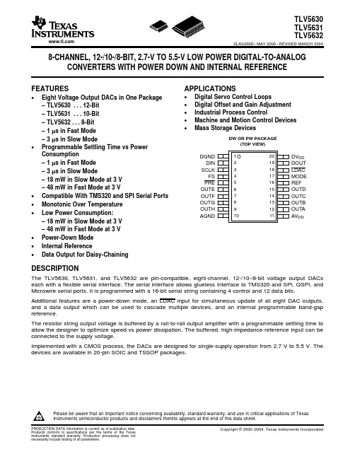
FEATURES APPLICATIONSDW OR PW PACKAGE(TOP VIEW)DESCRIPTIONTLV5630TLV5631TLV5632SLAS269D–MAY2000–REVISED MARCH2004 8-CHANNEL,12-/10-/8-BIT,2.7-V TO5.5-V LOW POWER DIGITAL-TO-ANALOG CONVERTERS WITH POWER DOWN AND INTERNAL REFERENCE•Digital Servo Control Loops •Eight Voltage Output DACs in One Package•Digital Offset and Gain Adjustment –TLV5630...12-Bit•Industrial Process Control–TLV5631...10-Bit•Machine and Motion Control Devices –TLV5632...8-Bit•Mass Storage Devices–1µs in Fast Mode–3µs in Slow Mode•Programmable Settling Time vs PowerConsumption–1µs in Fast Mode–3µs in Slow Mode–18mW in Slow Mode at3V–48mW in Fast Mode at3V•Compatible With TMS320and SPI Serial Ports•Monotonic Over Temperature•Low Power Consumption:–18mW in Slow Mode at3V–48mW in Fast Mode at3V•Power-Down Mode•Internal Reference•Data Output for Daisy-ChainingThe TLV5630,TLV5631,and TLV5632are pin-compatible,eight-channel,12-/10-/8-bit voltage output DACs each with a flexible serial interface.The serial interface allows glueless interface to TMS320and SPI,QSPI,and Microwire serial ports.It is programmed with a16-bit serial string containing4control and12data bits.Additional features are a power-down mode,an LDAC input for simultaneous update of all eight DAC outputs, and a data output which can be used to cascade multiple devices,and an internal programmable band-gap reference.The resistor string output voltage is buffered by a rail-to-rail output amplifier with a programmable settling time to allow the designer to optimize speed vs power dissipation.The buffered,high-impedance reference input can be connected to the supply voltage.Implemented with a CMOS process,the DACs are designed for single-supply operation from2.7V to5.5V.The devices are available in20-pin SOIC and TSSOP packages.Please be aware that an important notice concerning availability,standard warranty,and use in critical applications of TexasInstruments semiconductor products and disclaimers thereto appears at the end of this data sheet.元器件交易网OUTAREFSCLK DIN FS MODE DOUTOUT PREB, C, D,E, F , G and HTLV5630TLV5631TLV5632SLAS269D–MAY 2000–REVISED MARCH 2004These devices have limited built-in ESD protection.The leads should beshorted together or the device placed in conductive foam during storage or handling to prevent electrostatic damage to the MOS gates.AVAILABLE OPTIONSFUNCTIONAL BLOCK DIAGARAMTerminal Functions元器件交易网ABSOLUTE MAXIMUM RATINGS RECOMMENDED OPERATING CONDITIONSTLV5630TLV5631TLV5632 SLAS269D–MAY2000–REVISED MARCH2004over operating free-air temperature(unless otherwise noted)(1)(1)Stresses beyond those listed under,,absolute maximum ratings”may cause permanent damage to the device.These are stress ratingsonly,and functional operation of the device at these or any other conditions beyond those indicated under,,recommended operatingconditions”is not implied.Exposure to absolute-maximum-rated conditions for extended periods may affect device reliability.元器件交易网ELECTRICAL CHARACTERISTICSTLV5630TLV5631TLV5632SLAS269D–MAY 2000–REVISED MARCH 2004over recommended operating conditions (unless otherwise noted)(1)Power supply rejection ratio at full scale is measured by varying AV DD and is given by:PSRR =20log [(E G (AV DD max)-E G (AV DD min))/V DD max](2)In parallel with a 100-nF capacitor元器件交易网DIGITAL INPUT TIMING REQUIREMENTSTLV5630TLV5631TLV5632SLAS269D–MAY 2000–REVISED MARCH 2004ELECTRICAL CHARACTERISTICS (continued)over recommended operating conditions (unless otherwise noted)(3)Reference feedthrough is measured at the DAC output with an input code =0x000.(4)Settling time is the time for the output signal to remain within ±0.5LSB of the final measured value for a digital input code change of 0x080to 0xFFF and 0xFFF to 0x080,respectively.Assured by design;not tested.(5)Settling time is the time for the output signal to remain within ±0.5LSB of the final measured value for a digital input code change of one count.The max time applies to code changes near zero scale or full scale.Assured by design;not tested.(6)Slew rate determines the time it takes for a change of the DAC output from 10%to 90%full-scale voltage.(7)Code transition:TLV5630-0x7FF to 0x800,TLV5631-0x7FCto 0x800,TLV5632-0x7F0to 0x800.元器件交易网TYPICAL CHARACTERISTICS− O u t p u t V o l t a g e − VSinking Current − mAV O Sinking Current − mA− O u t p u t V o l t a g e − VV O− O u t p u t V o l t a g e − VV O Sourcing Current − mA− O u t p u t V o l t a g e − VV O Sourcing Current − mATLV5630TLV5631TLV5632SLAS269D–MAY 2000–REVISED MARCH 2004OUTPUT LOAD REGULATIONOUTPUT LOAD REGULATIONFigure 1.Figure 2.OUTPUT LOAD REGULATIONOUTPUT LOAD REGULATIONFigure 3.Figure 4.元器件交易网−4−3−2−10123401024204830724096I N L − I n t e g r a l N o n l i n e a r i t y − L S BCode−1.0−0.8−0.6−0.4−0.2−0.00.20.40.60.81.001024204830724096D N L − D i f f e r e n t i a l N o n l i n e a r i t y − L S BCode−2.0−1.5−1.0−0.50.00.51.01.52.002565127681024I N L − I n t e g r a l N o n l i n e a r i t y − L S BCodeTLV5630TLV5631TLV5632SLAS269D–MAY 2000–REVISED MARCH 2004TYPICAL CHARACTERISTICS (continued)TLV5630INTEGRAL NONLINEARITYvs CODEFigure 5.TLV5630DIFFERENTIAL NONLINEARITYvs CODEFigure 6.TLV5631INTEGRAL NONLINEARITYvs CODEFigure 7.元器件交易网−1.0−0.8−0.6−0.4−0.2−0.00.20.40.60.81.002565127681024D N L − D i f f e r e n t i a l N o n l i n e a r i t y − L S BCode−0.5−0.4−0.3−0.2−0.100.10.20.30.40.5050100150200250I N L − I n t e g r a l N o n l i n e a r i t y − L S BCode−0.5−0.4−0.3−0.2−0.100.10.20.30.40.5050100150200250D N L − D i f f e r e n t i a l N o n l i n e a r i t y − L S BCodeTLV5630TLV5631TLV5632SLAS269D–MAY 2000–REVISED MARCH 2004TYPICAL CHARACTERISTICS (continued)TLV5631DIFFERENTIAL NONLINEARITYvs CODEFigure 8.TLV5632INTEGRAL NONLINEARITYvs CODEFigure 9.TLV5632DIFFERENTIAL NONLINEARITYvs CODEFigure 10.元器件交易网PARAMETER MEASUREMENT INFORMATIONSCLKDINDOUT FS FS†Previous input data(µC mode)LDACOUTxTLV5630TLV5631TLV5632SLAS269D–MAY 2000–REVISED MARCH 2004Figure 11.Serial Interface TimingFigure 12.Output Timing元器件交易网APPLICATION INFORMATIONGENERAL FUNCTION2REF CODE 0x1000[V]SERIAL INTERFACESCLK FSDIN SCLK FSDINDSP Mode:µC Mode:TLV5630TLV5631TLV5632SLAS269D–MAY 2000–REVISED MARCH 2004The TLV5630/31/32are 8-channel,single-supply DACs,based on a resistor string architecture.They consist of a serial interface,a speed and power-down control logic,an internal reference,a resistor string,and a rail-to-rail output buffer.The output voltage (full scale determined by reference)for each channel is given by:where REF is the reference voltage and CODE is the digital input value.The input range is 0x000to 0xFFF for the TLV5630,0x000to 0xFFC for the TLV5631,and 0x000to 0xFF0for the TLV5632.A power-on-reset initially puts the internal latches to a defined state (all bits zero).A falling edge of FS starts shifting the data on DIN starting with the MSB to the internal register on the falling edges of SCLK.After 16bits have been transferred,the content of the shift register is moved to one of the DAC holding registers,depending on the address bits within the data word.A logic 0on the LDAC pin is required to transfer the content of the DAC holding register to the DAC latch and to update the DAC outputs.LDAC is an asynchronous input.It can be held low if a simultaneous update of all eight channels is not needed.For daisy-chaining,DOUT provides the data sampled on DIN with a delay of 16clock cycles.Difference between DSP mode (MODE =N.C.or 0)and µC (MODE =1)mode:•In µC mode,FS needs to be held low until all 16data bits have been transferred.If FS is driven high beforethe 16th falling clock edge,the data transfer is cancelled.The DAC is updated after a rising edge on FS.•In DSP mode,FS needs to stay low for 20ns and can go high before the 16th falling clock edge.•In DSP mode there needs to be one falling SCLK edge before FS goes low to start the write (DIN)cycle.This extra falling SCLK edge has to happen at least 5ns before FS goes low,t su(CK-FS)≥5ns.•In µC mode,the extra falling SCLK edge is not necessary.However,if it does happen,the extra negativeSCLK edge is not allowed to occur within 10ns after FS goes HIGH to finish the WRITE cycle (t su(FS-C17)).元器件交易网SERIAL CLOCK FREQUENCY AND UPDATE RATEf sclkmax+1t whmin)t wlmin+30MHzf updatemax+116ǒt whmin)t wlminǓ+1.95MHz DATA FORMAT TLV5630 TLV5631 TLV5632SLAS269D–MAY2000–REVISED MARCH2004 APPLICATION INFORMATION(continued)The maximum serial clock frequency is given by:The maximum update rate is:Note,that the maximum update rate is just a theoretical value for the serial interface,as the settling time of the DAC has to be considered also.The16-bit data word consists of two parts:•Address bits(D15 (12)•Data bits(D11 0Ax:Address bits.See table.REGISTER MAP元器件交易网DAC A-H AND TWO-CHANNEL REGISTERSPRESETTLV5630TLV5631TLV5632SLAS269D–MAY 2000–REVISED MARCH 2004Writing to DAC A-H sets the output voltage of channel A-H.It is possible to automatically generate the complement of one channel by writing to one of the four two-channel registers (DAC A and B etc.).The TLV5630decodes all 12data bits.The TLV5631decodes D11to D2(D1and D0are ignored).The TLV5632decodes D11to D4(D3to D0are ignored).The outputs of all DAC channels can be driven to a predefined value stored in the Preset register by driving the PRE input low.The PRE input is asynchronous to the clock.CTRL0PD :Full device power down 0=normal 1=power down DO :DOUT enable 0=disabled 1=enabledR1:0:Reference select bits 0=external 1=external,2=internal 1V,3=internal 2V IM :Input mode 0=straight binary1=twos complementX:ReservedIf DOUT is enabled,the data input on DIN is output on DOUT with a 16-cycle delay.That makes it possible to daisy-chain multiple DACs on one serial bus.CTRL1P XY :Power Down DAC XY 0=normal 1=power down S XY :Speed DAC XY0=slow1=fastXY:DAC pair AB,CD,EF or GHIn power-down mode,the amplifiers of the selected DAC pair are disabled and the total power consumption of the device is significantly reduced.Power-down mode of a specific DAC pair can be selected by setting the P XY bit within the data word to 1.There are two settling time modes:fast and slow.Fast mode of a DAC pair is selected by setting S XY to 1and slow mode is selected by setting S XY to 0.元器件交易网元器件交易网元器件交易网IMPORTANT NOTICETexas Instruments Incorporated and its subsidiaries (TI) reserve the right to make corrections, modifications,enhancements, improvements, and other changes to its products and services at any time and to discontinueany product or service without notice. Customers should obtain the latest relevant information before placingorders and should verify that such information is current and complete. All products are sold subject to TI’s termsand conditions of sale supplied at the time of order acknowledgment.TI warrants performance of its hardware products to the specifications applicable at the time of sale inaccordance with TI’s standard warranty. T esting and other quality control techniques are used to the extent TIdeems necessary to support this warranty. Except where mandated by government requirements, testing of allparameters of each product is not necessarily performed.TI assumes no liability for applications assistance or customer product design. Customers are responsible fortheir products and applications using TI components. T o minimize the risks associated with customer productsand applications, customers should provide adequate design and operating safeguards.TI does not warrant or represent that any license, either express or implied, is granted under any TI patent right,copyright, mask work right, or other TI intellectual property right relating to any combination, machine, or processin which TI products or services are used. Information published by TI regarding third-party products or servicesdoes not constitute a license from TI to use such products or services or a warranty or endorsement thereof.Use of such information may require a license from a third party under the patents or other intellectual propertyof the third party, or a license from TI under the patents or other intellectual property of TI.Reproduction of information in TI data books or data sheets is permissible only if reproduction is withoutalteration and is accompanied by all associated warranties, conditions, limitations, and notices. Reproductionof this information with alteration is an unfair and deceptive business practice. TI is not responsible or liable forsuch altered documentation.Resale of TI products or services with statements different from or beyond the parameters stated by TI for thatproduct or service voids all express and any implied warranties for the associated TI product or service andis an unfair and deceptive business practice. TI is not responsible or liable for any such statements.Following are URLs where you can obtain information on other Texas Instruments products and applicationsolutions:Products ApplicationsAmplifiers Audio /audioData Converters Automotive /automotiveDSP Broadband /broadbandInterface Digital Control /digitalcontrolLogic Military /militaryPower Mgmt Optical Networking /opticalnetworkMicrocontrollers Security /securityTelephony /telephonyVideo & Imaging /videoWireless /wirelessMailing Address:Texas InstrumentsPost Office Box 655303 Dallas, Texas 75265Copyright 2004, Texas Instruments Incorporated。
低频低噪声高增益放大器

低频低噪声高增益放大器——设计与报告总结2022年7月15日目录:一.方案设计与论证A.题目要求和指标分析B.信号源部分C.前级放大部分D.滤波器部分E.压控放大模块F.功率放大模块G.负反响放大模块二.电路设计A.整体电路设计B.信号源部分C.前级放大部分D.滤波器部分E.压控放大部分F.功率放大部分G.负反响部分三.测试方法与测试结果a.仿真部分b.实测部分本次设计是以vca810,op07,tda2030,msp430为核心器件的低频低噪声放大器。
带宽为3kHz~5kHz,电压放大系数可达200~2000倍,能保证波形不失真,噪声系数小,性能良好。
信号由自制正弦波振荡器产生,经过前级放大,再经vca810进展压控放大,而后经过3阶有源切比雪夫带通滤波器,最后经过tda2030为核心的功率放大器,输出给负载。
而由Msp430单片机进展AD采样和DA输出,实现负反响。
设计方案具有放大倍数高,预置步长小,低噪声,数字显示精度高等特点,到达了设计要求,实在可行。
一.方案论证1.题目要求和指标分析根据题目要求,设计方案应该实现电压放大,预置步进,数字显示,并且信号的通频带要在3kHz~5kHz,低噪声。
综合各项设计指标,将该系统设计为以下模块:信号发生模块,前级放大模块,步进放大模块,滤波器模块,功率放大模块,反响模块;详细设计框图如下:2. 信号源部分方案1:以为LM358为核心的正弦波振荡器,优点是元器件少,本钱低,稳定性好,失真度小,幅度频率可调,常用于音频电路。
方案2:采用555芯片设计,由555定时器所构成的多谐振荡器产生方波,方波经过积分电路产生三角波,三角波再经过差分放大电路的非线性转换产生正弦波。
设计过程较繁琐。
方案3:采用ICL8038芯片设计,该芯片是专用的函数发生芯片,波形原理上和555类似,集成度高,可以很好的实现波形的产生,且稳定度高,失真低,但本钱较高。
充分考虑本钱,设计难易,以及设计要求等指标,选择方案1;3. 前级放大部分方案1:利用低噪声运放OP37搭建的同相放大器,元件少,放大效果明显,原理简单,是目前最为常见的放大模块。
5638详细介绍

6.5 12位串行D/A转换器TLV5638应用实例6.5.1 TLV5638简介TLV5638是TI公司的12位D/A转换器,具有两个输出通道,数据传输接口为3线的串行接口,该接口能够与常用的微控制器或者微处理器直接相连。
每次传输数据由16位的数据组成一帧,其中4位控制命令字,12位输出数据。
TLV5638输出经过两个缓冲器,DAC的可编程建立时间使得设计人员能够优化速度与功耗分配的关系。
同时内置片上电压参考源,该参考源最大能达到1mA的电流,因此也可以将其作为整个系统的参考源,减少了系统设计的复杂性。
1.基本特性参数TLV5638的基本特性参数如下:● 12位分辨率;●双输出通道;●可编程内部参考源;●可变成速度(建立时间):快速模式1μs;慢速模式3.5μs;●兼容SPI串行接口;●差分非线性度<0.5LSB;●供电电源:2.7V~5.5V DC。
2.引脚配置TLV5638的引脚配置如图9-10所示。
9-10 TLV5638的引脚配置TLV5638的引脚功能说明:● DIN:串行数据输入● SCLK:串行接口时钟输入● /CS:片选信号输入,低电平有效● OUTA:A通道模拟电压输出● AGND:模拟地● REF:模拟电压参考输入/输出● OUTB:B通道模拟电压输出● VDD:供电电源(2.7V~5.5V)3.功能性说明TLV5638输入数据字长为16位,由两部分组成,如表9-4所示,其中,D15~D12为命令位,D11~D0为12位数据。
表9-4 TLV5638的16位数据字其中,SPD为速度模式选择,当SPD为高时,选择快速模式,当SPD为低时,选择慢速模式;PWR为电源模式设置,当PWR为高时,为掉电模式,当PWR为低时,为正常模式;R1与R0一起组成对TLV5638内部寄存器的选择,如表9-5所示。
表9-5 R1、R0选择内部寄存器当选择了 9-5中前面3个中的一个,即写数据到DACB、BUFFER或者DACA,则16位数据字中的后12位(D11~D0)为要写入的数据。
AD转换芯片介绍

l???????ADS7812?低功耗串行12位采样模数转换器
l???????ADS7810?12位800kHz采样CMOS模数转换器
l???????ADS7800?12位3us采样模数转换器
l???????ADS574??兼容微处理器的采样CMOSA/D转换器?
l???????THS1007?10位6MSPS同步采样四路通道ADC;包含并行DSP/uPI/F通道自动扫描?
l???????ADS901??10位20MSPSADC,具有单端/差动输入、外部参考和可调节全范围?
l???????ADS900??10位20MSPSADC,具有单端/差动输入、内部基准和可调节全范围?
l???????ADS822?10位40MSPSADC,具有单端/差动输入、内/外基准和断电、引脚符合ADS823/6/8?
l???????ADS821?10位40MSPSADC,单端/差动输入具有内部基准和9.3位ENOB?
l???????ADS820?10位20MSPSADC,单端/差动输入具有内部基准和9.5位ENOB?
l???????TLC3545?14位200KSPSADC,具有串行输出、自动断电和伪差动输入?
l???????TLC3544?14位、5V、200KSPS、4通道单级性ADC
l???????TLC3541?14位200KSPSADC系列输出、自动断电、单端输入?
l???????THS1403?14位、3MSPSADC单通道、差动输入、DSP/uPIF、可编程增益放大器、内部S&H?
l???????TLC4541?16位200KSPSADC,具有串行输出、自动断电和单端输入
tlv5638
Copyright © 1999–2004, Texas Instruments Incorporated
TLV5638
SLAS225C – JUNE 1999 – REVISED JANUARY 2004
This integrated circuit can be damaged by ESD. Texas Instruments recommends that all integrated circuits be handled with appropriate precautions. Failure to observe proper handling and installation procedures can cause damage.
FEATURES
• Dual 12-Bit Voltage Output DAC • Programmable Internal Reference • Programmable Settling Time:
– 1 µs in Fast Mode, – 3.5 µs in Slow Mode • Compatible With TMS320 and SPI™ Serial Ports • Differential Nonlinearity <0.5 LSB Typ • Monotonic Over Temperature
OUT B
7
REF
6
SCLK
2
VDD
8
TLV5638
Terminal Functions
SLAS225C – JUNE 1999 – REVISED JANUARY 2004
I/O/P
DESCRIPTION
TLV5638中文数据手册
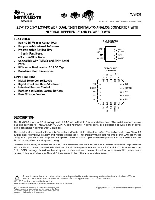
T L V5638中文数据手册TLV5638中文数据手册By Hi_Cracker @whu2.7-V至5.5 V低功耗双通道12位,具有内部参考电压和掉电模式的数模转化器Features:双通道12位电压输出DAC内部参考电压可编程稳定时间可编程:快速模式下 1us低速模式下 3.5us与TMS320和SPIE串行端口兼容差分非线性度典型值<0.5 LSB温度单调性Applications数字伺服控制回路偏移和增益的数字调整工业过程控制机械和运动控制设备大容量存储设备DescriptionTLV5638是一款双通道12位电压输出DAC,具有灵活的3线串行接口。
串行接口允许与TMS320和SPIE,QSPIE,MicrowireE通信协议的串行端口进行无缝连接。
它是通过16位串行字符串来完成编程的,其中包含4位控制字和12个数据位。
电阻串的输出电压经由增益为2的轨对轨输出缓冲器缓冲后输出。
该缓冲器具有AB类输出级,因此,提高了稳定性并减少了建立时间。
DAC建立时间的可编程,使设计师能够将速度与功耗进行最优化的处理。
凭借其片上可编程的精密电压基准,TLV5638简化了整个系统的设计。
由于其源输出能力可高达1 mA,所以其片上参考电压也可以用来作为一个系统参考电压使用。
采用CMOS工艺实现,该设备单电源工作,工作电压从2.7V至5.5 V。
它的封装形式是8-pin SOIC封装,在标准的商用,工业和汽车温度范围内的应用中,都大大减少了电路板空间。
在军用温度范围内的应用中,它采用了JG和FK封装。
Terminal FunctionsAGND:地CS:芯片选通。
数字输入低电平有效,用于使能/禁止输入。
DIN:串行数字输入。
OUTA:DAC A 通道模拟电压输出端OUTB:DAC A 通道模拟电压输出端REF:模拟参考电压输入输出端SCLK:数字串行时钟输入端VDD:供电电压输入端APPLICATION INFORMATIONgeneral functionTLV5638是一个双12位通道,基于串式电阻结构的单电源供电DAC。
TLV5608IYE资料
AVAILABLE OPTIONSIMPORTANT NOTICETexas Instruments Incorporated and its subsidiaries (TI) reserve the right to make corrections, modifications, enhancements, improvements, and other changes to its products and services at any time and to discontinue any product or service without notice. Customers should obtain the latest relevant information before placing orders and should verify that such information is current and complete. All products are sold subject to TI’s terms and conditions of sale supplied at the time of order acknowledgment.TI warrants performance of its hardware products to the specifications applicable at the time of sale in accordance with TI’s standard warranty. Testing and other quality control techniques are used to the extent TI deems necessary to support this warranty. Except where mandated by government requirements, testing of all parameters of each product is not necessarily performed.TI assumes no liability for applications assistance or customer product design. Customers are responsible for their products and applications using TI components. To minimize the risks associated with customer products and applications, customers should provide adequate design and operating safeguards.TI does not warrant or represent that any license, either express or implied, is granted under any TI patent right, copyright, mask work right, or other TI intellectual property right relating to any combination, machine, or process in which TI products or services are used. Information published by TI regarding third-party products or services does not constitute a license from TI to use such products or services or a warranty or endorsement thereof. Use of such information may require a license from a third party under the patents or other intellectual property of the third party, or a license from TI under the patents or other intellectual property of TI.Reproduction of information in TI data books or data sheets is permissible only if reproduction is without alteration and is accompanied by all associated warranties, conditions, limitations, and notices. Reproduction of this information with alteration is an unfair and deceptive business practice. TI is not responsible or liable for such altered documentation.Resale of TI products or services with statements different from or beyond the parameters stated by TI for that product or service voids all express and any implied warranties for the associated TI product or service and is an unfair and deceptive business practice. TI is not responsible or liable for any such statements. Following are URLs where you can obtain information on other Texas Instruments products and application solutions:Products ApplicationsAmplifiers Audio /audioData Converters Automotive /automotiveDSP Broadband /broadbandInterface Digital Control /digitalcontrolLogic Military /militaryPower Mgmt Optical Networking /opticalnetwork Microcontrollers Security /securityTelephony /telephonyVideo & Imaging /videoWireless /wirelessMailing Address:Texas InstrumentsPost Office Box 655303 Dallas, Texas 75265Copyright 2003, Texas Instruments Incorporated。
新国标电动汽车的直流充电桩控制系统设计
新国标电动汽车的直流充电桩控制系统设计孙涛;曹淑琴【摘要】根据目前国内电动汽车直流快充的现状,设计出了符合新国标GB/T18487.1-2015等5项国家标准的电动汽车直流快速充电桩.首先介绍了目前电动汽车充电方式的现状和新国标的特点,在此基础上,按照新国标的要求,提出了充电桩控制系统的总体设计架构,并从硬件和软件两个方面详细描述了有关设计.充电桩控制以STM32F103VE单片机作为核心,以μC/OS Ⅱ为嵌入式操作系统的底层控制程序,实现充电协议与输出控制功能.人机交互以WinCE触摸显示模组为核心,基于WinCE的人机交互界面,实现充电计费和操作指引功能.%According to the situation of DC charging pile for electronic vehicles in the domestic,a DC charging pile for electronic vehiclesis designed,that confirmes five national standards including GB/T18487.1-2015 etc.Firstly,the situation of DC charging pile and features of new national standard are introduced.And based on requests of new national standard,a structure of charging pile is designed and some project details from hardware and software are introduced.The charging pile takes STM32F103VE as the control core.And the μC/OS Ⅱ is used as the low-layer control program of embedded operating system.It achieves charging protocol and output control.The human-computer interface takes the WinCE touch display module as the core.It implementes the charging and operation guide function.【期刊名称】《单片机与嵌入式系统应用》【年(卷),期】2018(018)002【总页数】5页(P63-66,71)【关键词】充电桩;电动汽车;STM32F103VE;WinCE【作者】孙涛;曹淑琴【作者单位】北方工业大学电子信息工程学院,北京100141;北方工业大学电子信息工程学院,北京100141【正文语种】中文【中图分类】TP29引言电动汽车在行驶过程中,不会造成排气污染,对环境保护和空气洁净都是十分有益的。
启珑微电子产品手册说明书
产品手册PRODUCT MANUAL(北京︶有限公司并一直致力于为工业智能控制、医疗设备、轨道交通、智能交通以及智能家居等领域提供更优质的产品与服务。
公司具有深厚的文化底蕴,由多位有欧美留学、工作经历的归国人员创办,坚实的理论功底和丰富的芯片设计经验奠定了启珑微电子的高起点和高水准,并迅速成长为业内具有自主知识产权的中国IC设计品牌之一。
产品手册01序号产品型号封装形式产品概述兼容型号1CLM811HST-AXC TQFP-48SL811HST-AXC 2CLCP82C55AZ DIP-40CP82C55AZ 3CLIP82C55AZ DIP-40IP82C55AZ 4CLCS82C55AZ PLCC-44CS82C55AZ 5CLIS82C55AZ PLCC-44IS82C55AZ 6CLCQ82C55AZ MQFP-44CQ82C55AZ 7CLIQ82C55AZ MQFP-44IQ82C55AZ 8CLID82C55AZ DIP-40ID82C55A 9CLMD82C55A/B DIP-40MD82C55A/B 10CLMD82C55QA DIP-40MD82C55QA 11CLM65HVD230D SOIC-8SN65HVD230D 12CLM65HVD230QD SOIC-8SN65HVD230QD 13CLM65HVD231D SOIC-8SN65HVD231D 14CLM65HVD231QD SOIC-8SN65HVD231QD 15CLM65HVD232D SOIC-8SN65HVD232D 16CLM65HVD232QD SOIC-8SN65HVD232QD 17CLM65HVD233D SOIC-8具有待机模式和环回功能的 3.3V SN65HVD233D 18CLM65HVD233HD SOIC-8具有待机模式和环回功能的 3.3V SN65HVD233HD 19CLM65HVD233QDRQ1SOIC-8具有待机模式和环回功能的 3.3V SN65HVD233QDRQ120CLM65HVD233MDREP SOIC-8具有待机模式和环回功能的 3.3V SN65HVD233MDREP产品手册02序号产品型号封装形式产品概述兼容型号21CLM65HVD234D SOIC-8SN65HVD234D 22CLM65HVD234QDRQ1SOIC-8SN65HVD234QDRQ123CLM65HVD235D SOIC-8SN65HVD235D 24CLM65HVD235QDRQ1SOIC-8SN65HVD235QDRQ125CLM75176BPS SOIC-8SN75176BPSR 26CLM75176BDR SOIC-8SN75176BDR 27CLM75176ADR SOIC-8SN75176ADR 28CLM75176AP DIP-8SN75176AP 29CLM76176BP DIP-8SN75176BP 30CLM75179BPS SOIC-8SN75179BPS 31CLM75179BDR SOIC-8SN75179BDR 32CLM75179AP DIP-8SN75179AP 33CLM75179BP DIP-8SN75179BP 34CLM65HVD08D SOIC-8SN65HVD08D 35CLM65HVD08P DIP-8SN65HVD08P 36CLM65HVD75D SOIC-8具有IEC ESD保护功能和20Mbps的SN65HVD75D 37CLM65HVD75DGK VSSOIC-8具有IEC ESD保护功能和20Mbps的SN65HVD75DGK 38CLM65HVD75DRBT VDFN-8具有IEC ESD保护功能和20Mbps的SN65HVD75DRBT 39CLM3085CPA+DIP-8(10Mbps)、限摆率RS-485/MAX3085CPA+40CLM3085EPA+DIP-8(10Mbps)、限摆率RS-485/MAX3085EPA+产品手册03序号产品型号封装形式产品概述兼容型号41CLM3085EEPA DIP-8(10Mbps)、限摆率RS-485/MAX3085EEPA 42CLM3085CSA+T SOIC-8(10Mbps)、限摆率RS-485/MAX3085CSA+43CLM3085ECSA+T MSOIC-8(10Mbps)、限摆率RS-485/MAX3085ECSA+T 44CLM3085ESA+T SOIC-8(10Mbps)、限摆率RS-485/MAX3085ESA+45CLM3085EESA+T SOIC-8(10Mbps)、限摆率RS-485/MAX3085EESA+46CLM3088CSA+T SOIC-8MAX3088CSA+T 47CLM3088ECSA+T SOIC-8MAX3088ECSA+T 48CLM3088ESA+T SOIC-8MAX3088ESA+T 49CLM3088EESA+T SOIC-8MAX3088EESA+T 50CLM3088CPA+DIP-8MAX3088CPA+51CLM3088ECPA+DIP-8MAX3088ECPA+52CLM3088EPA+DIP-8MAX3088EPA+53CLM3088EEPA+DIP-8MAX3088EEPA+54CLM485CPA+DIP-8低功耗、限摆率、RS-485/RS-422MAX485CPA+55CLM485ECPA+DIP-8低功耗、限摆率、RS-485/RS-422MAX485ECPA+56CLM485EPA+DIP-8低功耗、限摆率、RS-485/RS-422MAX485EPA+57CLM485EEPA+DIP-8低功耗、限摆率、RS-485/RS-422MAX485EEPA+58CLM485CSA+SOIC-8低功耗、限摆率、RS-485/RS-422MAX485CSA+59CLM485ESA+SOIC-8低功耗、限摆率、RS-485/RS-422MAX485ESA+60CLM485EESA+SOIC-8低功耗、限摆率、RS-485/RS-422MAX485EESA+产品手册04序号产品型号封装形式产品概述兼容型号61CLM3490CSA+SOIC-8 3.3V供电、10Mbps、限摆率、真MAX3490CSA+62CLM3490ECSA+SOIC-8 3.3V供电、10Mbps、限摆率、真MAX3490ESA+63CLM3490ESA+SOIC-8 3.3V供电、10Mbps、限摆率、真MAX3490ESA+64CLM3490EESA+SOIC-8 3.3V供电、10Mbps、限摆率、真MAX3490EESA+65CLM3491CSD SOP-14 3.3V供电、10Mbps、限摆率、真MAX3491CSD+66CLM3491ECSD+SOP-14 3.3V供电、10Mbps、限摆率、真MAX3491ECSD+67CLM3491ESD+SOP-14 3.3V供电、10Mbps、限摆率、真MAX3491ESD+68CLM3491EESD+SOP-14 3.3V供电、10Mbps、限摆率、真MAX3491EESD+69CLM490CSA+SOIC-8低功耗、限摆率、RS-485/RS-422MAX490CSA+70CLM490ECSA+SOIC-8低功耗、限摆率、RS-485/RS-422MAX490ECSA+71CLM490ESA+SOIC-8低功耗、限摆率、RS-485/RS-422MAX490ESA+72CLM490EESA+SOIC-8低功耗、限摆率、RS-485/RS-422MAX490EESA+73CLM490CPA+DIP-8低功耗、限摆率、RS-485/RS-422MAX490CPA+74CLM490ECPA+DIP-8低功耗、限摆率、RS-485/RS-422MAX490ECPA+75CLM490EPA+DIP-8低功耗、限摆率、RS-485/RS-422MAX490EPA+76CLM490EEPA+DIP-8低功耗、限摆率、RS-485/RS-422MAX490EEPA+77CLM488CSA+SOIC-8低功耗、限摆率、RS-485/RS-422MAX488CSA+78CLM488ECSA+SOIC-8低功耗、限摆率、RS-485/RS-422MAX488ECSA+79CLM488ESA+SOIC-8低功耗、限摆率、RS-485/RS-422MAX488ESA+80CLM488EESA+SOIC-8低功耗、限摆率、RS-485/RS-422MAX488EESA+产品手册序号产品型号封装形式产品概述兼容型号81CLM488CPA+DIP-8MAX488CPA+82CLM488ECPA+DIP-8MAX488ECPA+83CLM488EPA+DIP-8MAX488EPA+84CLM488EEPA+DIP-8MAX488EEPA+85CLM232CSE SOIC-16MAX232CSE+T86CLM232ECSE SOIC-16MAX232ECSE+87CLM232ESE SOIC-16MAX232ESE+T88CLM232EESE SOIC-16MAX232EESE+T89CLM232CPE DIP-16MAX232CPE+90CLM232ECPE DIP-16MAX232ECPE+91CLM232EPE DIP-16MAX232EPE+92CLM232EEPE DIP-16MAX232EEPE+93CLM232CWE SOIC-16MAX232CWE+T94CLM232ECWE SOIC-16MAX232ECWE+T95CLM232EWE SOIC-16MAX232EWE+T96CLM232EEWE SOIC-16MAX232EEWE+T97CLM232ACWE SOIC-16MAX232ACWE+T98CLM232AEWE SOIC-16MAX232AEWE+99CLM3232CSE SOIC-16MAX3232CSE+T 100CLM3232ECSE SOIC-16MAX3232ECSE+T05产品手册06序号产品型号封装形式产品概述兼容型号101CLM3232ESE SOIC-16MAX3232ESE+T 102CLM3232EESE SOIC-16MAX3232EESE+T 103CLM1302S SOIC-8DS1302S+T&R 104CLM1302SN+SOIC-8DS1302SN+T&R 105CLM1302Z+T SOIC-8DS1302Z+T&R 106CLM1302ZN+SOIC-8DS1302ZN+T&R 107CLM1302+DIP-8DS1302+108CLM1302N+DIP-8DS1302N+109CLM307Z+SOIC-8DS1307Z+T&R 110CLM1307ZN+SOIC-8DS1307ZN+T&R 111CLM1307+DIP-8DS1307+112CLM1307N+DIP-8DS1307N+113CLM4717EUB+MSOP-10拟开关MAX4717EUB+114CLM231N/NOPB DIP-8LM231N/NOPB 115CLM231AN/NOPB DIP-8LM231AN/NOPB 116CLM331N/NOPB DIP-8LM331N/NOPB 117CLM331AN/NOPB DIP-8LM331AN/NOPB 118CLM298N Multiwatt-15L298N 119CLM298P POWERSO-20L298P 120CLM2543CDW SOIC-20TLC2543CDW产品手册07序号产品型号封装形式产品概述兼容型号121CLM2543IDW SOIC-20TLC2543IDW 122CLM2543CDB SSOP-20TLC2543CDB 123CLM2543IDB SSOP-20TLC2543IDB 124CLM2543CN DIP-20TLC2543CN 125CLM2543IN DIP-20TLC2543IN 126CLM1543CDW SOIC-20TLC1543CDW 127CLM1543IDW SOIC-20TLC1543IDW 128CLM1543CN DIP-20TLC1543CN 129CLM1543IN DIP-20TLC1543IN 130CLM5615CDGK VSSOIC-8趋稳时间为12.5us并具备上电复位功能的10位、单通道、低功耗DAC TLC5615CDGK 131CLM5615IDGK VSSOIC-8趋稳时间为12.5us并具备上电复位功能的10位、单通道、低功耗DAC TLC5615IGGK 132CLM5615CD SOIC-8趋稳时间为12.5us并具备上电复位功能的10位、单通道、低功耗DAC TLC5615CD 133CLM5615ID SOIC-8趋稳时间为12.5us并具备上电复位功能的10位、单通道、低功耗DAC TLC5615ID 134CLM5615CP DIP-8趋稳时间为12.5us并具备上电复位功能的10位、单通道、低功耗DAC TLC5615CP 135CLM5615IP DIP-8趋稳时间为12.5us并具备上电复位功能的10位、单通道、低功耗DAC TLC5615IP 136CLM3616-00SOP-14IW3616-00137CLM3616-01SOP-14IW3616-01138CLM3617-00SOP-14IW3617-00139CLM3617-01SOP-14IW3617-01140CLM3630-00SOP-14IW3630-00产品手册序号产品型号封装形式产品概述兼容型号141CLM1100-0001BGA-128ASIC从站控制ET1100-0001142CLM1100-0002BGA-128ASIC从站控制ET1100-0002143CLM1100-0003BGA-128ASIC从站控制ET1100-0003144CLM1200-0001QFN-48ASIC从站控制ET1200-0001145CLM1200-0002QFN-48ASIC从站控制ET1200-0002146CLM1200-0003QFN-48ASIC从站控制ET1200-0003147CLM8656ARZ SOIC-8AD8656ARZ148CLM8656ARMZ MSOIC-8AD8656ARMZ149CLM1040T/CM,118SOIC-8TJA1040T/CM,118 150CLM1042T/CM,118SOIC-8TJA1042T/CM,118 151CLM1050T/CM,118SOIC-8TJA1050T/CM,118 152CLM1051T/CM,118SOIC-8TJA1051T/CM,118 153CLM82C250T/YM SOIC-8PCA82C250T/YM 154CLM82C251T/YM SOIC-8PCA82C251T/YM 155CLMEE80C196KC20PLCC-68EE80C196KC20 156CLMEN80C196KC20PLCC-68EN80C196KC20 157CLMN80C196KC20PLCC-68N80C196KC20 158CLMTN80C196KC20PLCC-68TN80C196KC20 159CLMEE87C196KC20PLCC-68EE87C196KC20 160CLMEN87C196KC20PLCC-68EN87C196KC2008产品手册09序号产品型号封装形式产品概述兼容型号161CLMN87C196KC20PLCC-68N87C196KC20162CLMTN87C196KC20PLCC-68TN87C196KC20163CLM8051F020-GQ TQFP-100C8051F020-GQ 164CLM8051F021-GQ TQFP-64C8051F021-GQ 165CLM8051F330-GM VFQFN-20C8051F330-GM 166CLM8051F500-IQ TQFP-48C8051F500-IQ 167CLM8051F500-IM VFQFN-48C8051F500-IM 168CLM8051F502-IQ LQFP-32C8051F502-IQ 169CLM8051F502-IM QFN-32C8051F502-IM170CLM08D1500CIYB/NOPB HLQFP-128ADC08D1500CIYB/NOPB 171CLM083000CIYB/NOPB HLQFP-128ADCADC083000CIYB/NOPB 172CLM10AQ190AVTPY EBGA-38010位5GSPS ADC EV10AQ190AVTPY 173CLM9680BCPZ-1250LFCSP-64双通道14位1GSPS ADC AD9680BCPZ-1250174CLM9739BBCZ BGA-16014位、2.5 GSPS、RF数模AD9739BBCZ 175CLM9779ABSVZ TQFP-100双通道16位1GSPS DAC AD9779ABSVZ 176CLM12DS130AVZPY FPBGA-19612位3GSPS DAC EV12DS130AVZPY 177CLM12DS460AVZP FPBGA-19612位6.4GSPS DAC EV12DS460AVZP 178CLM9434BCPZ-370LFCSP-5612位370MSPS ADC AD9434BCPZ-370179CLM9434BCPZ-500LFCSP-5612位500MSPS ADC AD9434BCPZ-500180CLM4149IRGZTVQFN-4814位250MSPS ADCADS4149IRGZT产品手册10序号产品型号封装形式产品概述兼容型号181CLM9467BCPZ-200LFCSP-7216位200MSPS ADC AD9467BCPZ-200182CLM9467BCPZ-250LFCSP-7216位250MSPS ADC AD9467BCPZ-250183CLM9656BCPZ-125LFCSP-56四通道16位125MSPS ADC AD9656BCPZ-125184CLM9245BCPZ-40LFCSP-3214位40MSPS ADC AD9245BCPZ-40185CLM9245BCPZ-65LFCSP-3214位65MSPS ADC AD9245BCPZ-80186CLM9245BCPZ-80LFCSP-3214位80MSPS ADC AD9245BCPZ-80187CLM9783BCPZ LFCSP-72双通道16位500MSPS DAC AD9783BCPZ 188CLM7656BSTZ-REEL LQFP-64六通道16位250KSPS ADC AD7656BSTZ-REEL 189CLM7960BCPZLFCSP-3218位2MSPS ADC AD7960BCPZ190CLM128S102CIMTX/NOPB TSSOP-1612位1MSPS ADC ADC128S102CIMTX/NOPB 191CLM5638IDR SOIC-8DACTLV5638IDR 192CLM7606BSTZ LQFP-64AD7606BSTZ 193CLM9625BBPZ-2.5BGA-19612位2.6GSPS ADC AD9625BBPZ-2.5194CLM9164BBCZ BGA-16516位12GSPS DAC AD9164BBCZ 195CLM9154BCPZ LFCSP-88四通道16位2.4GSPS DAC AD9154BCPZ 196CLM2160IUK#PBF QFN-4816位25MSPS ADC LTC2160IUK#PBF 197CLM9652BBCZ-310BGA-144双通道16位310MSPS ADC AD9652BBCZ-310198CLM7779ACPZ-RL LFCSP-6424位16KSPS ADC AD7779ACPZ-RL 199CLM9208BBPZ-3000BGA-196双通道14位3GSPS ADCAD9208BBPZ-3000200CLM320VC33PGE120LQFP-144TMS320VC33PGE120产品手册序号产品型号封装形式产品概述兼容型号201CLM320VC33PGEA120LQFP-144TMS320VC33PGEA120 202CLM320VC33PGE150LQFP-144TMS320VC33PGE150203CLM320VC5402PGE100LQFP-144TMS320VC5402PGE100 204CLM320F28335PGFA LQFP-176TMS320F28335PGFA205CLM320LF2406APZA LQFP-100TMS320LF2406APZA206CLM320LF2406APZS LQFP-100TMS320LF2406APZS207CLM320LF2407APGES LQFP-144TMS320LF2407APGES208CLM320LF2407APGEA LQFP-144TMS320LF2407APGEA 209CLM320C6713BPYP200HLQFP-208TMS320C6713BPYP200 210CLM320C6713BZDP225BGA-272TMS320C6713BZDP225 211CLM320C6713BGDP225BGA-272TMS320C6713BGDP225 212CLM320C6713BZDP300BGA-272TMS320C6713BZDP300 213CLM320C6713BGDG300BGA-272TMS320C6713BGDP30011邮箱:*******************。
- 1、下载文档前请自行甄别文档内容的完整性,平台不提供额外的编辑、内容补充、找答案等附加服务。
- 2、"仅部分预览"的文档,不可在线预览部分如存在完整性等问题,可反馈申请退款(可完整预览的文档不适用该条件!)。
- 3、如文档侵犯您的权益,请联系客服反馈,我们会尽快为您处理(人工客服工作时间:9:00-18:30)。
TLV5638中文数据手册
By Hi_Cracker @whu
2.7-V至5.5 V低功耗双通道12位,具有内部参考电压
和掉电模式的数模转化器
Features:
双通道12位电压输出DAC
内部参考电压可编程
稳定时间可编程:
快速模式下1us
低速模式下3.5us
与TMS320和SPIE串行端口兼容
差分非线性度典型值<0.5 LSB
温度单调性
Applications
数字伺服控制回路
偏移和增益的数字调整
工业过程控制
机械和运动控制设备
大容量存储设备
Description
TLV5638是一款双通道12位电压输出DAC,具有灵活的3线串行接口。
串行接口允许与TMS320和SPIE,QSPIE,MicrowireE通信协议的串行端口进行无缝连接。
它是通过16位串行字符串来完成编程的,其中包含4位控制字和12个数据位。
电阻串的输出电压经由增益为2的轨对轨输出缓冲器缓冲后输出。
该缓冲器具有AB类输出级,因此,提高了稳定性并减少了建立时间。
DAC建立时间的可编程,使设计师能够将速度与功耗进行最优化的处理。
凭借其片上可编程的精密电压基准,TLV5638简化了整个系统的设计。
由于其源输出能力可高达1 mA,所以其片上参考电压也可以用来作为一个系统参考电压使用。
采用CMOS工艺实现,该设备单电源工作,工作电压从2.7 V至5.5 V。
它的封装形式是8-pin SOIC封装,在标准的商用,工业和汽车温度范围内的应用中,都大大减少了电路板空间。
在军用温度范围内的应用中,它采用了JG 和FK封装。
Terminal Functions
AGND:地
CS:芯片选通。
数字输入低电平有效,用于使能/禁止输入。
DIN:串行数字输入。
OUTA:DAC A 通道模拟电压输出端
OUTB:DAC A 通道模拟电压输出端
REF:模拟参考电压输入输出端
SCLK:数字串行时钟输入端
VDD:供电电压输入端
APPLICATION INFORMATION
general function
TLV5638是一个双12位通道,基于串式电阻结构的单电源供电DAC。
它包括一个串行接口,速度模式和掉电模式可控逻辑,可编程内部参考,电阻串,并具有轨至轨输出缓冲器。
输出电压(满刻度可以通过参考电压确定)由下式给出:
[v]
2 REF CODE
oX1000
这里REF是基准电压,CODE是数字输入值,范围为从0x000到0xFFF。
上电复位时把内部锁存器的值作为CODE的默认状态(所有位零)。
serial interface
CS的下降沿开始一位一位的将数据装入(从MSB位开始)内部寄存器,每来一个SCLK下降沿,装入一bit位数据。
在16位数据已经全部装入或CS上升时,移位寄存器的内容被移动到目标锁存器(DAC A,DAC B,BUFFER,CONTROL(控制)),取决于在数据字中的控制位。
关于SPIE和MicrowireE连接的注意事项:在控制器启动数据传输之前,软件必须在FS引脚产生一个下降沿。
如果字宽度是8位(SPIE,MicrowireE),必须在执行编程TLV5638之前进行两个写操作。
在写操作(s)之后,在第16时钟的上升沿,保持寄存器或控制寄存器会自动更新。
serial clock frequency and update rate
data format
register select bits
data bits: DAC A, DAC B and BUFFER
data bits: CONTROL
reference bits
Examples of operation
注意:以上几个内容可以直接查看TI官方数据手册
linearity, offset, and gain error using single ended supplies
当放大器的操作电压为单电源,电压偏移仍然可以是正的或负的。
一个正的偏移量,the output voltage changes on the first code change(?)。
负的偏移时,the output voltage may not change with the first code(?),取决于电压偏移的幅度。
输出放大器试图驱动输出得到一个负电压。
然而,由于负电源轨接地,输出电压不能低于负电源轨上的电压,故输出钳位为0 V。
所以输出电压保持在零,直到输入代码值产生足够的正输出电压,以克服负的偏移电压,故存在图14中所示的转移函数。
(en数据手册)
产生这样的断点是偏移量错误,而不是线性误差。
如果输出缓冲器可驱动得了,那么传递函数将可以达到地参考下面的虚线。
对于DAC,线性度的测量是在偏移和满量程误差都得到调整之后或以某种方式弥补这些误差之后,从全零输入(所有输入为0)到满量程输入(所有输入1)区间范围内的线性程度。
但是,单电源操作下不能对负偏移量在传递函数中产生的断点做出调整。
因此,线性度的测量测量范围是满量程代码和最低的代码之间能够产生正输出电压的那一部分。
definitions of specifications and terminology
integral nonlinearity (INL):
相对精度或积分非线性(INL),有时也称为线性误差,指的是实际输出和零点和满量程输出曲线之间的的最大偏差,这里不包括零点误差和满量程误差的影响。
differential nonlinearity (DNL):
差分非线性(DNL),有时也被称为差分误差,指的是任何两相差1 LSB的相邻代码产生的理想幅度与实际测量幅度之间的差异。
单调性是指在相同的方向上(或保持不变)输出电压的变化与数字输入码的变化之间的关系。
zero-scale error (EZS)
零刻度误差被定义为数字输入值0,与0 V输出之间的偏差
gain error (EG)
增益误差是DAC传递函数的斜率的误差。
total harmonic distortion (THD)
THD是6次谐波分量值与基本信号的rms值的比率。
THD值的单位是分贝。
signal-to-noise ratio + distortion (S/N+D)
S / N + D是输出信号的均方根值,与所有其他低于奈奎斯特频率成分的杂散信号(包括谐波但不包括直流输出信号)的均方根值之比。
S / N + D的值以分贝表示。
spurious free dynamic range (SFDR)
无杂散动态范围指的是输出信号均方根值和指定带宽内的最大杂散信号的rms值之间的差异。
无杂散动态范围(SFDR)的值以分贝表示。