材料物理112161358
2024年材料物理专业考研方向有哪些

2024年材料物理专业考研方向有哪些材料物理专业考研方向有哪些材料物理专业考研方向1:材料物理与化学专业介绍材料物理与化学专业(学科代码:080501)是物理、化学和材料等构成的交叉学科,它综合了各学科的研究方法与特色。
本学科是以物理、化学等自然科学为基础,从分子、原子、电子等多层次上研究材料的物理、化学行为与规律,研究不同材料组成-结构-性能间的关系,设计、控制及制备具有特定性能的新材料与相关器件,致力于先进材料的研究与开发。
是研究各种材料特别是各种先进材料、新材料的性能与各层次微观结构之间关系的基本规律,为各种高新技术材料发展提供科学依据的应用基础学科,是理工科结合的学科。
研究方向(1) 介电超晶格及其微结构材料与器件(2) 介电、铁电薄膜与集成器件(3) 人工带隙材料(4) 全氧化物异质结构与器件(5) 纳米材料与纳米电子学(6) 新型功能无机非金属材料(7) 微结构材料的设计(8) 材料设计中的高性能计算(9) 非线性光子学(10) 低维纳米材料的控制合成和组装(11) 生物纳米材料和生物医学材料(12) 纳米光子学材料就业前景材料物理与化学专业就业前景比较好,一是因为此专业既研究基础理论研究,更注重先进材料的研究与开发工作,再就是此专业涉及范围比较广泛,在各个行业都有很好的应用,所以此专业的就业面广。
此专业的毕业生可在多晶硅(化工能源公司)、半导体(电子类公司)、物理、材料类、无损检测(探伤、压力容器厂家)等行业就业。
另外在钢铁大型企业、飞机制造业、汽车制造业、IT相关产业等等,都需要精密的材料技术,就业前景看好。
就业方向(1) 在相关科研部门从事从事材料物理与化学领域的科研、教学与产品开发工作。
(2) 在高等院校与科研院所从事相关教学和研发工作(3) 工矿企业、贸易部门、政府机关从事科研、生产、检验和管理。
材料物理专业考研方向2:材料加工工程专业介绍材料加工工程(学科代码:080503)是材料科学与工程下设的二级学科之一。
《材料物理总复习》PPT课件
完整版课件ppt
72
完整版课件ppt
73
完整版课件ppt
50
完整版课件ppt
51
动画
完整版课件ppt
52
完整版课件ppt
53
完整版课件ppt
54
完整版课件ppt
55
完整版课件ppt
56
完整版课件ppt
57
完整版课件ppt
58
完整版课件ppt
59
完整版课件ppt
60
第六章 材料的声学
• 6.1 声波的产生与传播 • 6.2 室内声波和吸声材料 • 6.3 水中声学和水声材料 • 6.4 其他声学及其材料
完整版课件ppt
43
完整版课件ppt
44
完整版课件ppt
45
光在材料中传播时,遇到不均匀的结构产生的次级波, 与主波方向不一致,会与主波合成出现干涉现象,使光 偏离原来的方向,从而引起散射现象。
完整版课件ppt
46
完整版课件ppt
47
完整版课件ppt
48
动画
完整版课件ppt
49
完整版课件ppt
完整版课件ppt
41
完整版课件ppt
42
• 为什么金属材料的吸收系数大?而绝缘材 料的吸收系数小?
• 金属的价电子处于未满带,吸收光子后呈激发态,发生碰 撞而发热。金属和半导体吸收系数都很大。
• 绝缘体吸收系数小是由于其价电子所处的能带是满带的, 光子能量不足以使价电子跃迁到导带,在可见光波长区域 吸收系数小,但是在紫外光区域,光子能量越来越大,直 到光子能量达到禁带宽度,绝缘性材料的电子会吸收光子 能量从满带跃迁到导带,使其在紫外光区域吸收系数急剧 增大。
1-《材料物理性能》-第一章-概论

材料物理性能第一章:概论本节主要内容(一)材料及其性能研究的重要性(二)知识体系1、材料的概念2、材料的分类3、材料科学与工程专业(三)课程简介(四)第一章:材料物理性能概论材料及其性能研究:贯穿于整个人类的文明史。
人类使用的材料,决定了人类的文明程度。
实质上——主要取决于材料的性能如何。
材料的重要性Michael Faraday 电气时代:电磁材料超级计算机个人电脑材料是信息社会的基石!传感器件半导体芯片半导体技术液晶材料光学材料金属、高分子材料磁性材料移动通讯数码拍照拍照功能显示功能外壳信号接受对话功能电子线路照片存储介电材料移动网络语音、视频本节主要内容(一)材料及其性能研究的重要性(二)知识体系1、材料的概念2、材料的分类3、材料科学与工程专业(三)课程简介(四)第一章:材料物理性能概论◼材料(materials)的概念:➢材料是人类社会所能接受的、可经济地制造有用物品的物质。
➢材料是人类用于制造物品、器件、构件、机器或其他产品的物质的统称。
材料是人类赖以生存和发展的物质基础,与国民经济建设、国防建设和人民生活密切相关。
20世纪70年代,把信息、材料和能源誉为当代文明的三大支柱。
80年代,以高技术群为代表的新技术革命,又把新材料、信息技术和生物技术并列为新技术革命的重要标志。
◼材料的分类:➢按照人为加工程度区分:✓天然材料:自然界原来就有未经加工或基本不加工可直接使用•如棉花、沙子、石材、蚕丝、煤矿、石油、铁矿、羊毛✓合成材料:人为把不同物质经化学方法或聚合作用加工而成•如塑料、合成纤维和合成橡胶天然材料材料合成材料◼材料的分类:➢按照物理化学属性区分:✓金属材料✓无机非金属材料✓有机高分子材料✓复合材料➢按照用途区分:✓建筑材料、电子材料✓航空航天材料、核材料✓生物材料、能源材料✓。
金条铜阀玻璃水泥高分子材料碳纤维复合材料◼材料的分类:➢按照结晶状态区分:✓晶体(单晶、多晶):短程有序,长程有序✓非晶:短程有序,长程无序✓准晶:介于晶体和非晶之间,长程有序,但无平移对称性(如:5次旋转对称性)✓液晶:由固态向液态转化过程中存在的取向有序流体非晶玻璃NaCl 晶体2011诺贝尔化学奖“发现准晶体”[铝锰合金]达尼埃尔·谢赫特曼◼材料的分类:➢按照使用性能区分:◼复杂性能◼化学性能◼物理性能◼力学性能③使用性能②工艺性能①复合性能③抗渗入性②耐腐蚀性①抗氧化性④刚性③延性②韧性①强度⑥辐照性能⑤声学性能④光学性能③磁学性能②电学性能①热学性能结构材料功能材料新材料?知识体系◼材料科学与工程:是关于材料的➢组成与结构(composition and structure )➢合成与加工(synthesis and processing )➢基本性质(proporties )➢与服役性能(performance )这四个要素➢以及它们两两之间的互相联系的学科。
材料物理性能
研究目标
性能验证
评价检测
性能测试
设计
设计 依据 根底数据
供测试样
微组织 调节控制
组织表征 合成
10
结构
物质的结构:晶体的结构;晶体的缺陷;玻璃的结 构;固体的外表结构
材料的显微结构:在显微镜下直至电子显微镜下观 察到的结构组织;包括:相种类、多少、分布、晶 粒尺寸、形状;气孔大小和分布;杂质、缺陷、晶 界等。
❖ 导带且有禁带,故根本无 ❖ 导电能力。
半导体和绝缘体的区别
❖ 半导体和绝缘体的能带图的区别仅是禁带宽度的大 小。〔绝缘体:3ev~6ev, 半导体: 0.1 ev~2ev)
❖ 禁带宽度的大小就影响到自由电子数量的多少,禁 带宽度小,自由电子多,反之就少。
金属的导电性
❖ 金属的导电机制与马基申定那么 ❖ 当电子波在绝对零度下通过一个理想的晶体点
为了便于学习、测试和研究,常采用不同的标准来划分性能
程知识点很多,同学们需要预习,在课后及时 究竟是什么原因造成材料导电性的如此明显的差异呢?
与物质的能带结构及其被电子填充的性质有关
复习。 材料的电学性能大致上包含
复杂性能〔1〕复合性能:高温抗折强度、高温蠕变强度等 〔2〕工艺性能:可塑性、流动性等 〔3〕使用性能:耐磨性等 2K)的大小来评定金属的电学纯度。 前言〔Introduction) 物质的结构:晶体的结构;
本课程成绩组成:期末试卷60%〔闭卷〕+平 材料力学、固体物理导论、工艺学
根这底个是 电:阻物在理绝学对、零化度学时等降学为科零,。是这些学科在材料性能方面的应用
时作业、考勤、问答〔20%〕+随堂实验 本课程主要内容〔Contents〕
高温时金属的电阻率根本上取决于ρ(T),而在低温时取决于ρ残。
《材料物理性能》课后习题答案.doc
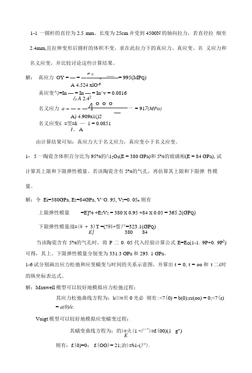
1-1 一圆杆的直径为2.5 mm、长度为25cm并受到4500N的轴向拉力,若直径拉细至2.4mm,且拉伸变形后圆杆的体积不变,求在此拉力下的真应力、真应变、名义应力和名义应变,并比较讨论这些计算结果。
解:真应力OY = — = ―"°。
—=995(MP Q)A 4.524 xlO-6真应变勺=In — = In — = In^v = 0.0816/0 A 2.42名义应力a = — = ―4°°°_ 一= 917(MPa)A) 4.909x1()2名义应变£ =翌=& —1 = 0.0851I。
A由计算结果可知:真应力大于名义应力,真应变小于名义应变。
1- 5 一陶瓷含体积百分比为95%的/\12O3(E = 380 GPa)和5%的玻璃相(E = 84 GPa), 试计算其上限和下限弹性模量。
若该陶瓷含有5%的气孔,再估算其上限和下限弹性模量。
解:令Ei=380GPa, E2=84GPa, V^O. 95, V2=0. 05o则有上限弹性模量=E]% +E2V2 = 380 X 0.95 +84 X 0.05 =365.2(GP Q)下限弹性模量战=(¥ +3)T =(?料+誓尸=323.1(GP Q)E]380 84当该陶瓷含有5%的气孔时,将P二0. 05代入经验计算公式E=E O(1-1. 9P+0. 9P2) 可得,其上、下限弹性模量分别变为331.3 GPa和293. 1 GPa。
1-6试分别画出应力松弛和应变蠕变与时间的关系示意图,并算出t = 0, t = oo和t二£时的纵坐标表达式。
解:Maxwell模型可以较好地模拟应力松弛过程:其应力松弛曲线方程为:b⑴=贝0光必则有:<7(0) = b(0);cr(oo) = 0;<7(r)= a(0)/e.Voigt模型可以较好地模拟应变蠕变过程:其蠕变曲线方程为:的)=火(1 -广")=£(00)(1 _g")E则有:£(0)=0; £(OO)= 21;冶)=%1-(尸).以上两种模型所描述的是最简单的情况,事实上山于材料力学性能的复杂性,我们会用到 用多个弹簧和多个黏壶通过串并联组合而成的复杂模型。
材料物理性能(课件)
TIM
Ni(OH)2
19
(二)热容
■ 热分析方法 · 差热分析(Differential thermal analysis, DTA): 测量试样与参比物之 间温差与时间或温度的关系 。分析所采用的参比物应是热惰性物质 , 即在 整个测试温度范围内不发生分解、相变和破坏 ,也不与被测物质发生化学 反应 。参比物的热容、热传导系数等应尽量与试样接近。
5
(一 )热学性能的物理基础
■ 晶格热振动
· 晶格热振动: 晶体点阵中质点围绕平衡位置的微小振动 。材料 热学性能的物理本质均与其晶格热振动相关。 · 晶格振动是三维的 , 当振动很微弱时 , 可认为原子作简谐振动。 振动频率随弹性模量Em增大而提高。
x=ACOS(ot+p)
· 温度升高时质点动能增大 , 1/2 mv2= 1/2 kT, ∑ (动能)i =热能 · 质点热振动相互影响 ,相邻质点间的振动存在一定的相位差, 晶格振动以波(格波) 的形式在整个材料内传播 。格波在固体中的 传播速度: v = 3 * 103m/s, 晶格常数a为10-10 m数量级 ,格波最高频 率:v / 2a = 1.5 * 1013 Hz · 频率极低的格波: 声频支振动; 频率极高的格波: 光频支振动
■ 亚稳态组织转变为稳定态要释放 热量 ,热容 -温度曲线向下拐折。
H
TC
T
二级相变焓和热容随温度的变化
17
(二)热容
■ 热容的测量
· 量热计法 。低温及中温区: 电加热法 · 高温区:撒克司法
P:搅拌器 ,C: 量热器筒 18
材料物理性能讲义

Ω Ω* = (2π)3
Rl • Kn = 2π(n1l1 + n2l2 + n3l3) = 2πm, m 为整数。
(2.5)
图 2.3 二维六角点阵的魏格纳-赛茨元胞(Wigner-Seitz 原胞)。
4
由于元胞是组成点阵的最小重复单元,根据点阵中每个格点附近环境的自相 似性即平移对称性我们可以推断, 只要在一个元胞内研究材料的物理特性就代表 研究了整个点阵结构的物理特性,为此我们定义一特殊的高对称元胞,它包含了 晶 格 点阵 点群 的 全部对 称 性。 这一 特 殊的高 对 称性 元胞 称 为魏格 纳 - 赛 茨
2π ( a 2 × a3 ) Ω 2π b2 = (a3 × a1 ) Ω 2π b3 = (a1 × a2 ) Ω b1 =
(2.3)
其中Ω = a1 • (a2 × a3)是正点阵元胞的体积。 在倒点阵中任一格点的位置矢可表示 为: Kn = n1b1 + n2b2 + n3b3
(2.4)
其中 n1, n2, n3 是整数,倒点阵元胞的体积为Ω* = b1 • (b2 × b3),且存在以下关系
图 2.4 从分立的原子轨道到固体能带结构的转变。
要理解固体的能带结构首先要从原子的电子轨道讲起,因为固体的能带归根 结底起源于原子的轨道能级。 根据量子力学,原子中带负电的电子绕带正电的原 子核运动,其轨道能量是不连续、分立的,如图 2.4 所示。在一定条件下如原子 间存在相互影响,同一原子中几个能量相近的不同类型的电子轨道(即波函数), 可以进行线性组合, 重新分配能量和确定空间方向, 组成数目相等的新电子轨道,
《材料物理化学性能》 物理性能部分
邓振炎 上海大学物理系 (电话:66134334,邮箱:zydeng@)
材料物理_李志林_期末试题2及答案
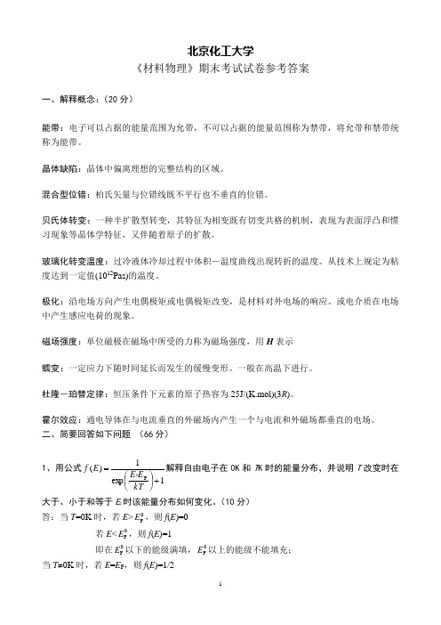
北京化工大学《材料物理》期末考试试卷参考答案一、解释概念:(20分)能带:电子可以占据的能量范围为允带,不可以占据的能量范围称为禁带,将允带和禁带统称为能带。
晶体缺陷:晶体中偏离理想的完整结构的区域。
混合型位错:柏氏矢量与位错线既不平行也不垂直的位错。
贝氏体转变:一种半扩散型转变,其特征为相变既有切变共格的机制,表现为表面浮凸和惯习现象等晶体学特征,又伴随着原子的扩散。
玻璃化转变温度:过冷液体冷却过程中体积-温度曲线出现转折的温度。
从技术上规定为粘度达到一定值(1012Pas)的温度。
极化:沿电场方向产生电偶极矩或电偶极矩改变,是材料对外电场的响应。
或电介质在电场中产生感应电荷的现象。
磁场强度:单位磁极在磁场中所受的力称为磁场强度,用H 表示 蠕变:一定应力下随时间延长而发生的缓慢变形。
一般在高温下进行。
杜隆-珀替定律:恒压条件下元素的原子热容为25J/(K.mol)(3R )。
霍尔效应:通电导体在与电流垂直的外磁场内产生一个与电流和外磁场都垂直的电场。
二、简要回答如下问题 (66分)1、用公式1ex p 1)(F +⎪⎭⎫ ⎝⎛=kT E-E E f 解释自由电子在0K 和T K 时的能量分布,并说明T 改变时在大于、小于和等于E F 时该能量分布如何变化。
(10分)答:当T =0K 时,若E >0F E ,则f (E )=0若E <0F E ,则f (E )=1即在0F E 以下的能级满填,0F E 以上的能级不能填充;当T ≠0K 时,若E =E F ,则f (E )=1/2若E < E F ,则当E << E F 时,f (E )=1;E F -E ≤kT 时f (E )<1 若E >E F ,则当E >> E F 时,f (E )=0;E -E F <kT 时f (E )<1/2即能量接近E F 的部分电子可以跃升到E F 以上,能量远离E F 的能级仍是满填的。
- 1、下载文档前请自行甄别文档内容的完整性,平台不提供额外的编辑、内容补充、找答案等附加服务。
- 2、"仅部分预览"的文档,不可在线预览部分如存在完整性等问题,可反馈申请退款(可完整预览的文档不适用该条件!)。
- 3、如文档侵犯您的权益,请联系客服反馈,我们会尽快为您处理(人工客服工作时间:9:00-18:30)。
A study on phononic crystalsAbstract: As is known to all, phononic crystal is a new type of acoustic functional material, which is necessary to be used in some special occasions, the study of phononic crystals caused a great deal of attention in the national research institutes. This article introduces the concept and the basic characteristics of phononic crystals in detail, the phononic crystal defects state characteristics, the phononic crystals forbidden band mechanism and various potential application areas (noise and vibration reduction) in phononic crystals. Finally, we prospect the research and development of the phononic crystals.Keywords: phononic crystals noise and vibration reduction prospect 1 IntroductionThe potential field of semiconductor atoms arranges periodically. When the propagation of the electrons happen in the semiconductor, the interaction between electronics and atomic periodic potential makes semiconductor electronic occupy band gap, which is able to manipulate the flow of electrons. On behalf of the silicon crystal semiconductor has brought a revolution in science and technology. With the development of the transistors, integrated circuits, large-scale integrated circuits even ultra-large-scale integrated circuits, semiconductor technology has a profound impact on the progress of human civilization [1,2].More than ten years ago, people began to touch on the opticalproperties of the structure and function of materials research. Theory and experiments have proved that if the dielectric of the material is a constant, the structure and function in the periodic variation in the optical wavelength scale, the interaction of photons with periodic structure makes the material has a similar semiconductor electronic band-gap energy band structure, called photonic band gap (known as photonic band gap). Periodic dielectric photonic band gap structure and function of materials are called photonic crystal (photonic crystals). Photon energy falls on the light waves in the photonic band gap can not be in the photon propagation in the crystal. When the photonic crystal exists (or introduced) point defects or line defects, the forbidden band of light waves will be localized in the point defect or only along the defect propagation. The design of the periodic structure of the photonic crystal and its defects, can artificially regulate the flow of photons[3].In 1987, the concept of photonic crystals independently proposed by E. Yabionovithch and S. John two[4]. In 1991, Yabionovitch verified the exist of microwave photonic band gap by experimental. Photonic crystal then quickly became photoelectron and information technology research in the field hot spots. Subsequently, it is discovered that when the elastic wave propagation exists in periodic elastic composite medium, it will have a similar elastic wave band, therefore, putting forward the concept of phononic crystals. Phononic crystal has a wealth of physicalconnotation and potentially broad application prospects. Phononic crystals have caused great concern of national research institutions[5].2Phononic crystals2.1The concepts and basic characteristics of phononic crystalsThe Phononic crystal is the cyclical nature of the elastic wave band structure and function of materials[6]. Phononic crystal internal material component (called groups) of the elastic constants and mass density parameters cyclical changes. With the band gap of the material components with different periodic structures in the form of different phonon crystal elastic wave characteristics are different.Phononic crystals have similar basic characteristics: when the elastic wave frequency falls within the band gap range, the elastic wave is prohibition of the dissemination, when there exists a point defect or line defect, the elastic wave is localized at the point defects, or only along the defect propagation[7]. Similarly, the design of the the phononic crystal periodic structure defects can artificially regulate the flow of elastic waves.Elastic wave is coupled by longitudinal and transverse waves full vector wave, three independent elastic parameters are in each group, that the mass density P, the longitudinal wave velocity Ci and shear wave wave velocity Ct (in the fluid medium, Ct =0); light wave is a scalar wave, only one independent elastic parameter is the dielectric constant in eachelement. The phononic crystals, therefore, possessing a richer physical meaning[8]. The following lists the relevant characteristics of the (electronic) crystals, photonic crystals and phonon crystals compared with three striking similarities can be seen from the table, the (electronic) crystals, photonic crystal research methods phonon crystals have a guiding role.According to the crystal structure of the phonons in the Cartesian coordinate system, in three orthogonal directions in the circumferential, periodic phononic crystals can be divided into one-dimensional, two-dimensional, three-dimensional phononic crystals. Scholars research has been carried out on some of the specific structure of phononic crystals: a one-dimensional phononic crystals, general periodic layered structure consisting of two or more materials; dimensional phononic crystals. Usually a certain direction is parallel to the space for the center axis of the cylinder material[9], and the periodicity of the lattice structure are formed in the buried base material, the cylinder material can be hollow or solid, generally circular cross-section of the cylinder, can also be square. Cylinder arrangement form may be a square arrangement, delta arrangement, the hexagonal array like dimensional phonon crystals are generally buried in a base material formed of a spherical scattering body periodic lattice structure, periodic lattice structures can be in the form of a body-centered cubic structure, face-centered cubic structure, hexagonalclose-packed structure. Figure 1 shows a typical schematic block diagram of the various phonon crystals.Fig 1 Phononic crystals of different dimensions2.2 The research overview of phononic crystalThe propagation characteristics of elastic waves in layered media research has been for nearly 70 years’ history, while the phononic crystals proposal of the concept and the theory of phonon crystal was just nearly 10-year history[10]. Phononic crystal researches, due to the difficulties of theoretical research, as well as other factors, making relatively slow progress and the crystal literature of total are no more than 150, according to incomplete statistics. In 1992, MM Signal and EN Economou first confirmed in theory that a spherical scattering body embedded in a matrix material to form a three-dimensional periodic lattice structure having elastic wave band gap characteristics[11]. In 1993, M. S. Kushwaha et.al first clear phononic crystals and the concept, and nickel column aluminum alloy forming the composite dielectric matrix, calculated by the plane wave method can be obtained in shear polarization direction ofelastic wave band. In 1995, R. Martinez-Sala et.al in the West Spain Madrid 200 years ago, a sculpture made flowing melody acoustic properties research, first confirmed the presence of the elastic wave band from the experimental point of view from this phonon crystal caused great concern[12]. Phononic crystal research work focuses on the formation of the band gap of phononic crystals and phase should the theoretical calculations[13]. In addition, scholars are from various countries in crystal defects phonon state study, experimental research has also been made good progress in applications of explore infancy . Phononic crystal research areas are in the country, Wuhan University and Guandong University of Science and Technology has made some progress. National University of Defense Technology Photonic/phononic crystal research center is currently engaged in the study of phononic crystals[14].2.3 Research content of phonon crystalsPhononic crystal researches mainly includes three aspects: the band gap of the phononic crystal mechanism, characteristics of defect states and application researches.2.3.1 phononic crystal band gap mechanismA lot of theoretical and experimental studies have proved the existence of a phononic crystal elastic wave band, Figure 2 shows a typical phonon crystal band structure, shaded in Figure 2 is the elastic wave band gap.Fig 2 An elastic band gap of a typical phononic crystalThere are two more mature about the mechanism of elastic wave band formed, scattering mechanisms and locally resonant mechanism in Prague. Bragg scattering leaded by crystal band theory in solid state physics, photonic crystals comply with the Bragg scattering mechanism. Bragg scattering caused by the band gap is mainly due to[15]: the cycle changing in material properties with elastic wave interaction, such that certain frequencies of the wave does not correspond to the vibration mode in the periodic structure, which can not spread, resulting in the forbidden band. Large number of studies of elastic wave band gap formed literature focuses on the Bragg scattering mechanism, the study shows that the elastic wave band gap generates composite media related component of the elastic constants, density and speed of sound, and the filling ratio of the component; and lattice structure and size. In general, non-network type of the lattice structure than network-type lattice structure is easy to produce the band gap; elastic component in the composite dielectric constant, the greater the difference, the more prone the forbidden band [16]. In addition, the wavelength of the elastic wave band correspondingBragg scattering formes of the elastic wave is usually associated with periodic structure, the size parameter (i.e, the lattice size or lattice constant) equivalent to the forbidden band is consistent with the mechanism in concept with the photonic crystal periodic structure. Bragg scattering mechanism phononic crystals at low frequencies (especially below 1khz), the application causes some difficulties.Liu Zhengyou et.al did research on viscoelastic soft materials with shot simple cubic lattice structure buried in the epoxy resin to form the three-dimensional phononic crystals found the phononic crystal band gap is much larger than the wavelength corresponding to the size of the lattice, breaking through the limitations of the Bragg scattering mechanism, and not strictly in the scatterer cycle distribution, even random distribution, the composite structure also has a band gap, and thus raise locally resonant elastic wave band mechanism[17]. Localized resonance mechanism, under the excitation of an elastic wave of a specific frequency, the single scattering body resonance, and the interaction with the incident, so that it can not continue to spread. Band-gap generation mainly depends on the individual single scattering body itself, the structure and the interaction of the elastic wave. Local resonance mechanism, phononic crystals, the vibration inherent characteristics of the band gap and single scattering body is closely related to the cyclical nature of the scattering body and the lattice constant has nothing to dowith it, and this has opened up a broad road in the application of the low-frequency band for phononic crystals.In a word, Bragg scattering mechanism emphasizes the periodic structure of the wave, and how to design the periodic structure of the lattice constant and the material component of the mix is one of the critical factors of the design band gap; localized resonance mechanism to emphasize the role of the special structure of the single scattering body wave, how to design the resonance structure of the single scatterer and scattering body in the spread characteristics of the base body is a key issue[18].Phononic crystal band gap mechanism relies on the calculation of the elastic wave band, the mature elastic wave band gap calculation method transfers matrix method, plane wave expansion method, finite different time domain method, multiple scattering method.2.3.2 Transfer matrix methodThe method used for the band gap of the one-dimensional phononic crystal (layered medium) calculation are very simple tools. Basic side of the transfer matrix method parameters from the contact state (stress, particle velocity, etc.) process to start, drawing the transfer matrix of the solid plate medium, and then by the surrounding medium and intermediate dielectric interface characteristics given boundary conditions, the solution of the system can be finally obtained. Because the transfer ofthe matrix is generally smaller, and catalytical solutions, so the smaller is the amount of calculation.In a real crystal, various couplings exist between the motions of electrons, photons, and phonons. For example, infrared absorption and polariton excitation results from the coupling between lattice vibrations and electromagnetic (EM) waves in an ionic crystal[19]. If the ferroelectric domain or piezoelectric coefficient is modulated in a phononic crystal, the interaction between the super lattice vibrations and EM wave may be established. Similar effects can be expected in such an artificial medium. This kind of phononic crystal is termed an ionic-type phononic crystal (ITPC).2.3.3 Plane wave expansion methodThis method can be used for two-dimensional and three-dimensional phononic crystals band-gap calculation. Plane wave method by the displacement in the wave equation, elastic parameters and other physical quantities in the reciprocal lattice vector space in the form of a plane wave superposition of approximate expand, the wave equation into an intrinsic equation solving eigenvalue can get the frequencies and wave vector between the dispersion relation, namely the so-called band structure[20]. Phononic crystals forbidden band structure calculations, the plane wave expansion method has been widely used. It can transfer from solid-solid, liquid(gas)-liquid (gas) in the calculation of other componentsof the various structures of the phonon crystal has achieved considerable success. Plane wave expansion method for phononic crystal band gap calculated convergence is slow, and phononic crystals constituted by the solid-liquid (gas) can not be accurately calculated, so it has some limitations.2.3.4 FDTD methodThis method can be used for two-dimensional and three-dimensional phononic crystals band gap calculation. FDTD[21] method is a direct time-domain discrete wave equation method to solve the differential equations, a problem of numerical methods for solving the band gap of the phononic crystal. The method can simulate a variety of complex periodic structure, the non-uniformity of the medium, anisotropy, dispersion characteristics and nonlinear problems can be accurately simulated. FDTD method phonon band-gap calculated phonon band-gap calculated with the use of multiple scattering method are in good agreement. We should pay attention to the numerical stability and convergence the calculated phonon crystals instantaneous nonlinear response problems.2.3.5 Multiple scattering methodThis method is mainly used for three-dimensional phononic crystal band gap. Multiple scattering method can calculate the energy band structure of the crystal depends on each ball between the elastic scatteringby calculation incident since the sound waves of the other ball to the the single ball surface scattering, can solve the characteristic frequency equation can also calculate the reflection and transmission coefficients of the elastic wave scattered body periodic array of finite-layer structure. The theory of multiple scattering method cited in the electronic band structure calculations KKR (korringa-kohn-roskoker), is very suitable for the calculation of the special structure (such as solid spheres dispersed in the fluid) the phonon crystals[22]. Calculating the phonon energy band structure of the crystal, the usual plane wave method can not give the exact solution. Multiple scattering method is complex and difficult to use.2.4 phonon characteristics of crystal defect statesBragg scattering mechanism of phonon crystals have ideal periodic structure, the destruction of this ideal periodic structure is generally referred to as the defects(the concept follows the solid-state physics about defects in concept). The defects can be classified according to their dimension point defects, line defects and surface defects. When the existence of a crystal phonon in defects so-called defect states in the band-gap range, defect states in existence will phononic crystals forbidden band features a significant impact the phononic crystal defect states characteristics of great significance[23]. MM Signals et.al study two-dimensional lead/epoxy phononic crystals exist of elastic wave propagation, the point defects with changing the diameter of a leadcolumn to obtain, the calculations show that point defects on the elastic wave has a local role. Kafesaki et.al used the finite-difference time-domain (FDTD) method to study the elastic waves in a two-dimensional lead/epoxy phononic crystals spread in the presence of line defects, the line defect phononic crystals in the removal of a row or a lead bar, and studies have shown that the elastic wave propagation only along the defect[24]. Experimental defect states, Torres et.al studied the surface states in the two-dimensional mercury/aluminum phononic crystals, pointed out that the sound waves of acoustic waves in phononic crystal interface localized phenomenon. Also with experimental research by removing some of the water silver.The formation of the silver column formed L-shaped line defect and piezoelectric vibrator instead of a mercury column the acoustic wave propagation in the case of point defects, the experiments show that sound waves only along the defect. Propagation or localized at the point defects, the experimental results well validate the theoretical calculation results. Defects study three-dimensional phononic crystals, only a theoretical work. Psarobas et.al in this paper three-dimensional shot in the epoxy matrix face-centered cubic array in the presence of surface defects makes the band gap of the phononic crystal in transverse waves and longitudinal waves localized phenomenon[25]. Crystal defect states in phonon, most are just theoretical calculation work. Band-gap calculation method is alsoa major plane wave method, finite difference time domain method, multiple scattering method. Phononic crystals have only point defects, line defects, surface defects, three kinds of missing notch forms, but they can have the form of a variety of structures for each defective form. The sound photonic crystal defect states characteristics will phononic crystal engineering applications to provide a wide range of theoretical guidance.2.5 phononic crystals applicationsThe phononic crystals used largely in the prospect stage, phonon crystal characteristics of the body has a band gap, defect states features make it the vibration, noise, acoustic devices, so has a potentially broad application prospects. Phononic crystals in damping characteristics of the forbidden band, high precision machinery without vibration in the processing system provides a certain frequency range within the processing environment, thus ensuring plus machining accuracy level; certain sophisticated equipment can also provide a certain frequency range vibration-free work environment, and to improve the accuracy of operating parameters, improve reliability, extend life. Noise reduction, the band gap of the phononic crystal characteristics, possible to design a new noise reduction materials and manufacturing. This material may be in the noise propagation isolation of noise on the way, they can control the noise at the noise source. According to the local resonance machine reasonable, if you break through the low-frequency band gap of the phononic crystaldesign phononic crystals in the latent. Anechoic tiles boats, sonar has a broad application prospects[26]. When some defects in phononic crystals forbidden in periodic structures are within the so-called defect states. According to the Bureau defective sonic phononic crystal domain characteristics, you can design a new type of high-efficiency, low-power acoustic filter can also be designed with features highly focused, low-power acoustic lens. Very little about the the phononic crystals applied research literature. As far as we know, currently there are only two articles on the work in this area: A. Diez and other people through the fiber engraved the eclipse acoustic grating one-dimensional phononic crystal fiber anticous-optic modulation; F. Cervera et.al elastic material arranged in the air constitute dimensional phononic crystals real now a the acoustic lens function[27]. We have also noted that the U.S. Defense Advanced Research Projects Agency (DARPA) in 1999 phononic crystal financial support for sound filter, vibration and noise isolation. With Phononic crystal theory research being mature, the phononic crystals applied research will also arouse more and more attention. The phononic crystals research will involve phononic crystal preparation theory and technology surgery phononic crystal test characterization, they are also a phononic crystal research. Although there is no specialized literature work in this area, but with the sound sub-crystal applied research work commenced, this part of the research work will be paid attention to.3 ConclusionsThe phononic crystals theoretical studies have just has a certain basis, applied research begun. Research on a large number of domestic and foreign literatures and based on our current work situation conditions, we believe that further research work on phononic crystals will include the following several aspects.(1) On the basis of the theoretical calculation of the existing phononic crystals forbidden band fully studied various structural forms, material properties, lattice size phononic crystal band gap characteristics phononic crystals forbidden band characteristics, and strive to be drawn with each correspondence between a function of the parameters (structure, material properties, lattice size, etc.), so as to realize the band gap of the phononic crystal design. Phononic crystal band gap.(2) Studying the introduction of the damping effect theory, and striving to accurately describe phonon crystal energy distribution (phononic crystal elastic wave transmission, absorption, reflection), and thus further reveal the role of phononic crystals mechanism.(3) Further study on the phononic crystal defect states in the propagation of elastic waves in a forbidden band calculation theory. (4) On the basis of the above work, explore phononic crystals in vibration, noise reduction, sound waves change can applications such research.The phononic crystals with a new acoustic functional materials has rich connotation of physical and potentially broad application prospects. The phononic crystals help us to broaden and deepen the understanding of the physical properties of the composite medium, find some new phenomena and new laws, the theoretical results obtained by the study will be to guide and to promote the application of phononic crystals, thus promoting human civilization progress.3 references【1】Joannopouios J D,Meade R D,Winn J N. Photonic Crystals [M].Princeton Univ Press,1995.【2】Yabionovitch E. [J] . Physical Review Letters,1987,58(20):2059.【3】John S. [J] . Physical Review Letters,1987,58(20):2486.【4】Signals M M,Economou E N. [J] . Journal of Sound and Vibration,1992,158 (2):377.【5】Kushwaha M S.P,Dobrzynsi L,et .al. [J] . Physical Review Letters,1993,71(13):2022.【6】Economou E N,Signals M M. [J] . Physical Review B,1993,48(18):134. 【7】Kushwaha M S.P,et al. [J] . Physical Review B,1994,49(4):2313. 【8】Munjal M L. [J] . Journal of Sound and Vibration,1993,162(2):333. 【9】Vasseur J,Djafari-Rouhani B,et al. [J] . Journal of Physics:Condensed Matter,1994,6:8759.【10】Martinez-Saia R,Sancho J,Sanchez J V,et ai. [J] . Nature,1995,378:241.【11】Signals M M,Soukouiis C M. [J] . Physical Review B,1995,51(5):2780. 【12】Kafesaki M,Economou E N. [J] . Physical Review B,1995,52(18):317. 【13】Kushwaha M S. P. [J] . Applied Physics Letter,1996,69(1)31.【14】Sigaias M M. [J]. Journal of the Acoustic Society of America,1997,101(3):1256.【15】Sigaias M M. [J] . Journal of Applied Physics,1998,84(6):3026.【16】Kushwaha M S,Djafari-Rouhani B. [J]. Journal of Applied Physics,1998,84(9):4677.【17】Sanchez-Perez J V,Cabaiiero D,et al. [J] . Physical Review Letters,1998,80(24):5325.【18】Torres M,Montero de Espinosa F R,et.al. [J] . Physical Review Letters,1999,82(15):3054.【19】Kafesaki M,Economou E N. [J] . Physical Review B,1999,60(17):11993. 【20】Kafesaki M,Sigaias M M,Garcfa N. [J] . Physical Review Letters,2000,85(19):4044.【21】Psarobas I E,Stefanou N,Modinos A. [J] . Physical Review B,2000,62 (1):278.【22】Liu Zhengyou,Chan C T,et ai. [J] . Physical Review B,2000,62(4)2446. 【23】Liu Zhengyou,Zhang Xixiang,et. Al. [J] . Science,2000,289:1734. 【24】Sigaias M M,Garcia N. [J] . Journal of Applied Physics,2000,87【25】Goffaux C,Vigneron J P. [J] . Physical Review B,2001,64(7):075118. 【26】Wu Fugen,Liu Zhenyou,Liu Youyan. [J] . Chinese Physics Letters,2001,18(6):785.【27】Cervera F,Sanchis L,et.al. [J] . Physical Review Letters,2002,12( 3 ): 82.。