基于AT91RM9200微控制器的以太网接口驱动程序设计
浅谈AT91RM9200的嵌入式网络摄像机的设计与实现

浅谈AT91RM9200的嵌入式网络摄像机的设计与实现1.引言随着通信技术和网络技术的迅猛进展,通过网络远程实时监控重要场所已倍受人们关注,网络摄像机在此背景下产生,并成为人们关注的焦点。
网络摄像机是一种结合传统摄像机与网络技术所产生的新一代摄像机,它可以将影像通过网络传至地球另一端,且远端的扫瞄者不需用任何专业软件,只要标准的网络扫瞄器(如"Microsoft IE或Netscape)即可监视其影像。
网络摄像机要将高清楚度的实时视频信息通过互联网传送到监控终端,因其信息量巨大,所以必需压缩。
通常人们采纳与MPEG-4算法相结合的计划来实现,不仅编程工作量大,而且产品的成本高。
本文所介绍的网络摄像机采纳专用的MPEG-4压缩芯片、以作为操作系统,不仅开发便捷、成本低廉,而且实时性好,适用范围广。
2.系统总体设计系统总体设计包括硬件设计和软件设计两部分。
这两部分工作是相互联系的,需要交错举行,系统设计是开发人员举行的工作,他们将系统设计阶段得到的目标系统的规律模型转换为目标系统的物理模型,该阶段得到工作成绩――系统设计解释书是下一个阶段系统实施的工作依据。
硬件设计模块主要包括微控制器模块、微控制器是将微型计算机的主要部分集成在一个芯片上的单芯片微型计算机。
微控制器出生于20世纪70年月中期,经过20多年的进展,其成本越来越低,而性能越来越强大,这使其应用已经无处不在,遍及各个领域。
例如电机控制、条码阅读器/扫描器、消费类、嬉戏设备、电话、HVAC、楼宇平安与门禁控制、工业控制与和白色家电(洗衣机、微波炉)等。
压缩编码模块、网络接口模块和相机控制模块四部分。
微控制器模块主要由主控芯片、DataFlash和SDRAM(1)组成。
其中,主控芯片是囫囵控制系统的核心,它负责囫囵系统的调度工作。
DataFlash里固化了嵌入式Linux内核、及其文件系统、应用软件和第1页共7页。
AT91RM9200(DKEK) VxWorks BSP
AT91RM9200(DK/EK) VxWorks BSP开发者指南AT91RM9200(DK/EK) VxWorks BSP (1)开发者指南 (1)1. 介绍: (1)2. 软件包安装: (2)3. BSP结构: (2)•逻辑结构 (2)•文件结构 (4)4. 编译与裁减BSP (5)5. 硬件配置 (7)6.程序流程 (8)7. 程序说明 (8)1) 基本 BSP (8)2) 中断控制器驱动(intrCtl) (12)3) 时钟驱动(timer) (13)4) Uart 驱动(sio) (14)5) 网络驱动(end) (14)6) usb Host驱动(usb) (16)7) usb slave驱动(usbslave) (16)8) Display驱动(display) (18)9) CompactFlash卡驱动(cf) (20)10) 声音codec驱动(audio) (23)11) DataFlash卡驱动(dataflash) (25)12) MMC 卡驱动(mmc) (28)1. 介绍:本软件是基于ATMEL AT91RM9200 评估板(AT91RM9200DK 和 AT91RM9200EK) 的VxWorks 操作系统的BSP.它包含以下功能.1) AT91RM9200 高级中断控制器(AIC)2) AT91RM9200 系统时钟3) 2 个UART .4) 1 个10/100M 以太网口5) USB host (OHCI)接口.6) USB Salve 接口7) 1个 CompactFlash 接口8) 1个 Atmel DataFlash/MMC 接口.9) 1个 DAC3550A 音频输出接口.10) Epson s1d13806 显示接口.2. 软件包安装:本软件包有两部分组成.一部分是BSP(at91rm9200bsp.zip), 另一部分是范例项目(at91rm9200proj.zip).把at91rm9200bsp.zip 直接解压到Vxworks操作系统安装目录下的target/config目录下. 解压后会出现at91rm9200目录.把at91rm9200proj.zip 直接解压到Vxworks操作系统安装目录下的target/proj目录下. 解压后会出现at91rm9200目录.3. BSP结构:• 逻辑结构本软件包有两部分组成.一部分是BSP, 另一部分是范例项目.BSP 位于Vxworks操作系统安装目录下的target/config/at91rm9200.范例项目位于Vxworks安装目录下的target/proj/at91rm9200.启动Tornado后,打开workspace, target/proj/at91rm9200/at91.wsp.在这个workspace中包含了项目 at91rm9200.wpj ,每个项目有三个视图(Files, Vxworks,Build).Files 视图列出了范例项目包含的文件,这些文件都是缺省的,基本上每一个项目都是一样的(参阅vxworks的手册)。
最新-SSD192019显示控制器与AT91RM9200的接口技术 精品

SSD1906显示控制器与AT91RM9200的接口技术摘要通过对1906显示控制器的介绍,分析其在基于919200微控制器的嵌入式系统中的应用;给出详细的硬件连接图及主要的寄存器配置。
关键词1906919200显示控制引言1906是公司推出的一款中小规模的显示控制芯片。
这款显示控制芯片集成了显存及时序电路,因而为手持设备和消费电子领域提供了一个低成本、低功耗的单芯片解决方案。
919200是公司推出的一款基于9的嵌入式处理器,时钟频率为180。
919200处理器内部没有集成控制器,因而需要通过专用的显示控制器,实现显示。
本文介绍1906显示控制器在基于919200微控制器的嵌入式系统中的具体应用。
11906显示控制器介绍1906显示控制芯片,内部集成了256的显存,可以支持单色和彩色,以及多种有源和无源面板。
1906还具有强大的总线兼容性,可与多种类型的连接。
此外,1906提供的功能还包括虚拟显示、浮动窗口窗口大小可变显示,并支持两个光标,可以减少软件的操作。
32位的内部数据通道,可以提供高带宽的显示内存,以实现现快速的屏幕刷新。
1906还个有单电压供电的优点。
1906显示控制器的另一个特点,是具有很短的访问延迟时间,因而可以支持无交互信号的微处理器。
此外,1906支持单时钟信号输入,即总线时钟、内存时钟和像素时钟都可以由时钟输入1得到。
这款显示控制器对的类型和操作系统没有具体要求,因而是实际应用中的一个理想的显示解决方案。
基于1906的显示控制系统结构如图1所示。
11总线兼容性1906显示控制器兼容多种类型的接口,特别是对现在常用的嵌入式处理器,基本上都可以实现无缝连接。
对于不同的总线接口,1906内部提供了多个时序控制寄存器,可以根据不同接口的时序要求,进行相应的配置。
1906支持的总线接口类型包括具有信号的通用#1型和通用#2型总线接口;;1龙珠;68;龙珠6832868328;日立3和4。
星光AT91RM9200开发板使用手册
中国电子开发网()星光AT91RM9200开发板使用手册用户手册CEDN2008‐4‐1在使用本文档的时候,如遇到问题请访问中国电子开发网的技术支持()目录星光AT91RM9200开发板使用手册 (3)0 结构示意图 (3)1 系统构成 (4)1.0 基本构成 (4)1.1 外部接口 (4)2 地址空间分配(系统reset之后) (4)3 外部中断分配 (5)4 跳线说明 (6)4.0 启动模式选择 (6)4.1 其他跳线(一般不必设置) (6)5 首次使用 (7)5.0 注意事项 (7)5.1 开发板板载启动代码 (7)5.2 开发板板载启动信息 (7)6 简单程序的调试 (8)6.0 调试工具 (8)6.1 AXD添加H‐JTAG支持 (8)6.2 调试过程 (9)7 将文件烧写到开发板 (12)7.0 将文件烧写到NOR FLASH (12)8 其他说明 (14)星光AT91RM9200开发板使用手册0 结构示意图图1、星光AT91RM9200开发板结构示意图1 系统构成1.0 基本构成1、处理器CPU: 型号AT91RM9200 封装272pin‐FBGA2、NOR FLASH: 型号SST39VF3201 封装48Pin‐TSOP 4M 总线宽带16bits3、NAND FLASH: 型号K9F1208U0C‐Y,P 封装48pin‐TSOP1 64M4、内存SDRAM: 型号HY57V281620 封装54pin‐TSOP 两片32M 总线宽带32bits 1.1 外部接口1、UART串口: 3个的串口(J3为4线,J4为2线(DEBUG),J15为485串口)。
2、USB接口: 1个USB Host接口。
1个USB Device接口。
3、IIC接口: 用于IIC总线EEPROM。
4、SD/MMC接口: 用于SD/MMC卡。
5、CF卡接口: 1个CF卡。
6、CAN总线: 通过SPI总线扩展,MCP2515 CAN控制器。
基于AT91RM9200与LINUX2.6.26内核的嵌入式平台开发全过程
基于AT91RM9200与LINUX2.6.26内核的嵌入式平台开发全过程收藏一、ARM9+LINUX开发历程使用了51系列和MOTOROLA单片机若干年,觉得自己已经跟不上嵌入式发展的时代了。
决定开发一种新的硬件平台,综合比较了一下,觉得ARM9+LINUX模式不错。
先从头捋一遍32位嵌入式开发平台的流程:芯片选型——使用DXP画原理图(如果有可能买块开发板可以极快加快进度)——使用DXP 画PCB图——芯片购买/PCB投板生产——芯片焊接——使用ADS编写简单硬件测试程序,调试硬件——搭建LINUX服务器,在服务器建立交叉编译环境——利用服务器和本机超级终端开发U-BOOT-1.3.4——利用U-BOOT-1.3.4的以太网FTP功能和服务器移植开发LINUX-2.6.26 内核——开发文件系统——开发驱动程序——应用程序开发,项目完基本成后回过头来想就是这个一个过程,中间走了不少弯路,在本博客中都有记载,很多问题有的也没有来得及记。
说干就干,时间安排如下:(1)5~7月硬件设计(芯片,型号,预测价格),已初步完成CPU:AT91RM9200,81SDRAM:MT48LC16M16A2TG-75IT(两片32MB*2)74*2FLASH:S29GL256N10TAI010(NOR型,32MB,存代码,写慢读快)57.52FLASH∶K9F2G08U0B(NAND256MB,预留存测试数据,写快读慢)41.1铁电存储器:FM24CL64(代替EEPROM24LC65,8KB)8.29以太网物理层控制器:DM9161E(100M/10M自适应)9.4从USB接口:用于与PC机通信主USB接口:用于后续移植LINUX时软件更新触摸屏驱动器:TSC2046(预留)液晶显示屏模块-TFT液晶显示接口(预留)(2)ADS+AXD+J-LINK调试过程目的是为了熟悉ARM开发流程,ADS开发环境,以便为将来U-BOOT的移植打下基础.由于网上资料不多,本步骤走了不少冤枉路,特总结在此,以便以后可以参考.容易步骤省略.安装ADS>>创建ADS工程>>添加所需要文件>>DEBUG SETTING,将程序的RO_Base设为0X200000则将程序导入A T91RM9200的片内16K的SRAM中运行,实践证明此时不需要管BMS引脚是高是低都能正常运行,也不需要进行REMAP;若将程序的RO_Base设为0X20000000则将程序导入片外64M的SDRAM中运行,此时程序导进SDRAM后需要SETMEM命令将SDRAM初始化,才能正常运行。
基于AT91RM9200微处理器的最小系统设计
研究Technology StudyI G I T C W 技术26DIGITCW2020.061 A RM 微处理器目前,在多个领域中都在使用ARM 微处理器,例如通信电子、智能工业、多媒体教育等。
根据相关数据统计,通用计算机的应用数据已经大大低于基于ARM 微处理器的设备应用数据。
故此,基于ARM 微处理器的开发应用已成为数字时代的应用技术潮流。
文章中主要介绍了基于AT91RM9200处理器的最小系统,其次介绍了ARM 芯片的外围接口的电路设计,并给出了相关器件选型。
2 硬件设计最小系统是最基本的电路,为了保证微处理器的工作可靠。
ARM 处理器最小系统的定义是确保ARM 处理器能够正常启动、运行的最小电路集合。
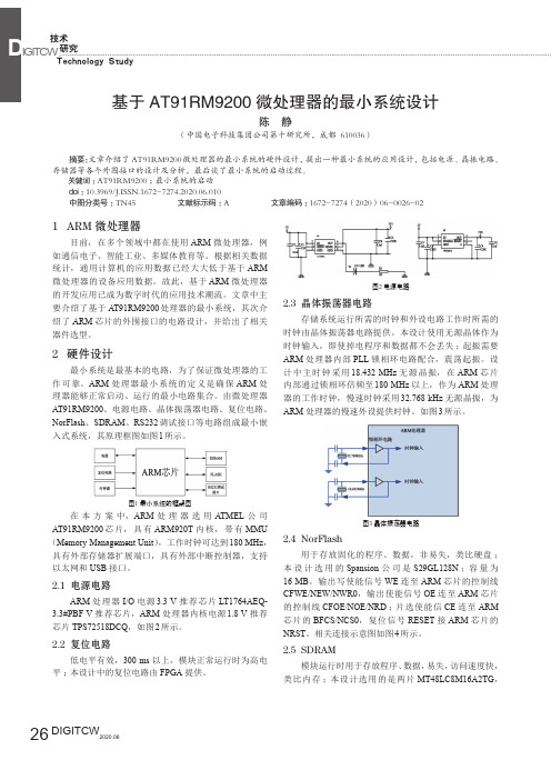
由微处理器AT91RM9200、电源电路、晶体振荡器电路、复位电路、NorFlash 、SDRAM 、RS232调试接口等电路组成最小嵌入式系统,其原理框图如图1所示。
图1 最小系统的框架图在本方案中,ARM 处理器选用ATMEL 公司AT91RM9200芯片,具有ARM920T 内核,带有MMU (Memory Management Unit ),工作时钟可达到180 MHz ,具有外部存储器扩展端口,具有外部中断控制器,支持以太网和USB 接口。
2.1 电源电路ARM 处理器I/O 电源3.3 V 推荐芯片LT1764AEQ-3.3#PBF V 推荐芯片,ARM 处理器内核电源1.8 V 推荐芯片TPS72518DCQ ,如图2所示。
2.2 复位电路低电平有效,300 ms 以上,模块正常运行时为高电平;本设计中的复位电路由FPGA提供。
图2 电源电路2.3 晶体振荡器电路存储系统运行所需的时钟和外设电路工作时所需的时钟由晶体振荡器电路提供。
本设计使用无源晶体作为时钟输入,即使掉电程序和数据都不会丢失;起振需要ARM 处理器内部PLL 锁相环电路配合,震荡起振。
设计中主时钟采用18.432 MHz 无源晶振,在ARM 芯片内部通过锁相环倍频至180 MHz 以上,作为ARM 处理器的工作时钟,慢速时钟采用32.768 kHz 无源晶振,为ARM 处理器的慢速外设提供时钟。
AT91RM9200DK U-Boot Flash Programming Solutions
AT91RM9200DK U-Boot Flash ProgrammingSolutionsIntroductionThe AT91RM9200DK Development Board is provided with a default boot program in its external Flash memory. This boot program, called U-Boot, is used by the AT91RM9200DK to boot after reset. The U-Boot performs initialization of the AT91RM9200DK, provides user interface via the Serial Debug Port and allows appli-cation download through the Serial Debug Port or Ethernet.This Application Note aims at providing solutions when the U-Boot program contained in the external Flash of AT91RM9200DK Development Board has been deleted. Two ways of reprogramming the Flash memory are described in this Application Note; the method selected depends on whether the user has a Slingshot™ JTAG/ICE interface. If this interface is not being used, then the external Flash is reprogrammed using the internal BootROM (embedded on the AT91RM9200 version 58A07F).AT91 ARM®Thumb®MicrocontrollersApplication Note6041A–ATARM–01/042AT91RM9200DK U-Boot Application Note6041A–ATARM–01/04U-Boot SoftwareFeatures The main features of the U-Boot software embedded in the AT91RM9200DK Develop-ment Kit are:•Standalone primary bootstrap •Small footprint •OS-independent •Auto-boot and interactive modes •Command line interface •Non-volatile environment variables •Flash programming capability •DataFlash programming capability (only available in latest Open Source download)•Download through serial interface (Kermit protocol)•Download through Ethernet (tftp)•Integrated bootp •Scripting capabilityOrganization To optimize the use of resources, U-Boot is made up of three parts:•A primary bootstrap •A de-compression executable • A gzip-compressed binary executable called the U-Boot ImageThe primary bootstrap is concatenated to the de-compression executable into one sin-gle file called the boot image and must reside in the AT91RM9200DK Flash on NCS0 ataddress 0x1000_0000.The primary bootstrap is a simple assembly code routine that sets up the system andputs it into an operational state. More specifically, it starts the high-speed clocks of theCPU and programs the on-chip memory controller to define the memory layout. Whenthese steps are completed, the primary bootstrap gives control to the de-compressionexecutable.The de-compression executable is an optimized version of the gunzip program. It de-compresses the gzip-compressed image of U-Boot into RAM, and jumps to it. The loca-tion of the binary executable in RAM is defined at link time.3AT91RM9200DK U-Boot Application Note6041A–ATARM–01/04Figure 1. Flash Mapping0x1000_0000Boot Image24 KbytesEnvironment Variables 8 Kbytes0x1000_E0000x1000_60000x1001_0000Free32 KbytesU-BootgzippedImage64 Kbytes0x1002_00004AT91RM9200DK U-Boot Application Note6041A–ATARM–01/04Reprogramming the External Flash on the AT91RM9200DK Development Board For Users of SlingshotJTAG/ICE Interface andMULTI ®2000The procedure for reprogramming the Flash described here is applicable to users of the AT91RM9200DK Development Board who have the Green Hills ® Slingshot JTAG/ICE interface and MULTI2000.Hardware and SoftwareRequirements •UBootFlashProgramming.zip file provided with this Application Note •Green Hills Slingshot JTAG/ICE interface •Green Hills MULTI2000 (V3.6.1 or higher) running on your PC •A serial cable (null modem)•HyperTerminal running on your PC application (1115200, 8, N, 1)Connecting theAT91RM9200DK to the HostPC 1.Connect the AT91RM9200DK to the Host PC using the serial cable through the Serial Debug Port on the A T91RM9200DK and the serial COM port on the Host PC. Open a HyperT erminal session with the following configuration: 115200 bitrate, 8-bit data length, No parity bit, 1 stop bit and No flux control.2.Connect the Slingshot JT AG/ICE Interface to the A T91RM9200DK through theJTAG/ICE Interface connector and to the PC through the USB Port.Launching the MULTI2000 3.Extract the AT91RM9200 Getting Started Software Package file calledAT91RM9200-GettingStarted-GHS3_6-1_1.exe , available in the UBootFlash-Programming.zip file provided with this Application Note.unch the MULTI2000 Project Manager and open the project Getting-Started.bld. This is available in the software package, extracted to the followingdirectory path C:\UBootFlashProgramming\AT91RM9200-GettingStarted-GHS3_6-1_1\A T91RM9200-GettingStarted\compil.5.Select the project basic_flash.bld by double-clicking on it. Build it and check ifbuild was succesful.6.Power-up and reset the AT91RM9200DK Development Board.Configuring the Connection to the AT91RM9200DK This is one of the most important steps in the procedure. As the Flash has been com-pletely erased, a standard initialization that would normally configure the External BusInterface, the Remap and the PLLs is not performed on the AT91RM9200DK. To carryout the initialization correctly, a Target Setup Script file (extension .dbs) must be used.The file, named mpserv_dk9200_PLL.dbs, is provided with this Application Note. Youare strongly advised to use it.To proceed:7.Click on the Connect button to open the Connection Chooser window:5AT91RM9200DK U-Boot Application Note6041A–ATARM–01/048.In the Connection Chooser window, select the ARM ®9 Green Hills Probe ™ Con-nection (mpserv):9.Edit the selected Connection Method:10.In the Slingshot Connection Editor window, select the Target Setup Script file thatinitializes the AT91RM9200DK correctly. It is very important to use the filempserv_dk9200_PLL.dbs provided with this Application Note:6AT91RM9200DK U-Boot Application Note6041A–ATARM–01/04Launching the Debugger 11.Click on the Debug button to run the debugger:12.In the debugger environment, click on the Step button to download thebasic_flash project:13.In the debugger environment, switch to the command pane:Loading the LoaderApplication The next step is to download the loader.bin application. This application is used to download a binary file from a HyperTerminal session through the Serial Debug Portusing the Xmodem protocol. The loader.bin file to download is available in the the soft-ware package extracted at the beginning of the procedure and available in the directory C:\UBootFlashProgramming\AT91RM9200-GettingStarted-GHS3_6-1_1\AT91RM9200-GettingStarted\Flash. See “Launching the MULTI2000” on page 4.14.Download the loader.bin application in the internal RAM at address 0x200000 bywriting the following command in the command pane window (prompt MULTI>):MULTI> memload raw C:\UBootFlashProgramming\AT91RM9200-GettingStarted-GHS3_6-1_1\AT91RM9200-GettingStarted\Flash\loader.bin 0x20000015.Set the Program Counter (pc) at the beginning of the downloaded loader.binapplication and run from here:MULTI> target reg pc 0x200000MULTI> target runLoading U-Boot The loader application is now running on the AT91RM9200DK and is ready to downloada binary application file through the Serial Debug Port using the Xmodem protocol on a HyperTerminal session.16.Download the u_boot.bin binary file using the Xmodem protocol. This file isavailable in the UBootFlashProgramming.zip file provided with this ApplicationNote under the directory path C:\UBootFlashProgramming\binary.7AT91RM9200DK U-Boot Application Note 6041A–ATARM–01/04In the HyperTerminal session, send the file u_boot.bin using the Xmodem protocol.At the end of the Xmodem transfer, a new prompt is displayed in the HyperTerminal window:Uboot>The U-Boot is now running on the AT91RM9200DK.This Boot program can now be used to download files to the SDRAM through the Serial Debug Port using the Kermit protocol with a HyperTerminal session. It is then copied to the Flash.Downloading U-Boot BinaryFiles The last step is to download the primary bootstrap, boot.bin, and the gzip-compressed U-Boot image, u-boot.gz. These two files are available in the UBootFlashProgram-m i ng.z i p fi l e pr o v i d e d w i t h t hi s A p pl i c a t io n N o te in th e d i r e c to r y C:\UBootFlashProgramming\binary.17.The first file to load is the boot image “boot.bin ”.Uboot> loadb 20000000## Ready for binary (Kermit) download …## Start Addr =0x20000000The boot image is now loaded in SDRAM. The following command copies the SDRAM (0x20000000) to Flash(0x10000000):Uboot> protect off 10000000 10005fffUnprotect 3 sectorsUboot> erase 10000000 10005fffErase Flash from 0x10000000 to 0x10005fff...Erasing sector 0 ... ok.Erasing sector 1 ... ok.Erasing sector 2 ... ok.done.Erased 3 sectors.Uboot> cp.b 20000000 10000000 5FFFCopy to flash… done.Uboot> protect on 10000000 10005FFFProtected 3 sectorsUboot>18.Once the primary bootstrap has been loaded, the U-Boot gzipped image can becopied into Flash. The file to load is the uboot gzipped image “u-boot.gz ”:Uboot> loadb 20000000## Ready for binary (Kermit) download …## Start Addr =0x20000000Uboot> protect off 10010000 1001ffffUnprotect 1 sectorsUboot> erase 10010000 1001ffffErase Flash from 0x10010000 to 0x1001ffff...8AT91RM9200DK U-Boot Application Note6041A–ATARM–01/04Erasing sector 8 ... ok.done.Erased 1 sectors.Uboot> cp.b 20000000 10010000 FFFFCopy to flash… done.Uboot> protect on 10010000 1001FFFFProtected 1 sectorsUboot>19.The U-Boot has been upgraded. Reboot your board.9AT91RM9200DK U-Boot Application Note6041A–ATARM–01/04Using the InternalBootROM The procedure for reprogramming the Flash described here is applicable to users of theAT91RM9200DK Development Board who do not have a Green Hills Slingshot JTAG/ICE Interface. The solution presented here uses the Internal BootROM of the AT91RM9200.After reset, the AT91RM9200DK boots from the external Flash memory by default (BMS high during reset). To boot using the embedded Boot ROM program (on-chip boot mode with BMS low during reset), it is mandatory to remove the R159 resistor from the AT91RM9200DK development board temporarily.Hardware and SoftwareRequirements •UBootFlashProgramming.zip file available with this Application Note •A serial cable (Null modem)•HyperTerminal running on your PC application (1115200,8,N,1)Connecting theAT91RM9200DK to the HostPC 1.Connect the AT91RM9200DK to the Host PC using the serial cable through the Serial Debug Port on the A T91RM9200DK and the serial COM port on the Host PC. Open a HyperT erminal session with the following configuration, 115200 bitrate, 8-bit data length, No parity bit, 1 stop bit and No flux control.Loading the Loader Application2.Download the loader.bin application. This application is used to download abinary file from a HyperTerminal session through the Serial Debug Port using the Xmodem protocol.3.Extract the AT91RM9200 Getting Started Software Package file calledAT91RM9200-GettingStarted-GHS3_6-1_1.exe , available on the UBootFlash-Programming.zip file provided with this Application Note. The loader.bin file to download is available in the software package extracted to the following directory path C:\UBootFlashProgramming\AT91RM9200-GettingStarted-GHS3_6-1_1\A T91RM9200-GettingStarted\Flash.4.Power-up and reset the AT91RM9200DK Development Board.The Internal Boot Program runs and waits for downloading an application code into the internal SRAM via Xmodem protocol through the Serial Debug Port (DBGU). It then branches to the application entry point at the first address of the SRAM.5.On the HyperTerminal session, send the file loader.bin using Xmodem protocol.Loading U-Boot The loader application is now running on the AT91RM9200DK and is ready to downloada binary application file through the Serial Debug Port using the Xmodem protocol on a HyperTerminal session.6.Download the u_boot.bin binary file using the Xmodem protocol. This file isavailable available in the UBootFlashProgramming.zip file provided with this Application Note under the following directory path C:\UBootFlashProgramming\binary.In the HyperTerminal session, send the file u_boot.bin using Xmodem protocol. At the end of the Xmodem transfer, a new prompt is displayed in the HyperTerminal window:Uboot>The UBoot is now running on the AT91RM9200DK.This Boot program can be used to download files to the SDRAM through the Serial Debug Port using the Kermit protocol with a HyperTerminal session. It is then copied to the Flash.10AT91RM9200DK U-Boot Application Note6041A–ATARM–01/04Downloading U-Boot BinaryFiles The last step is to download the primary bootstrap, boot.bin, and the gzip-compressed U-Boot image, u-boot.gz. These two files are also available in the UBootFlashProgram-m i ng.z i p fi l e pr o v i d e d w i t h t hi s A p pl i c a t io n N o te in th e d i r e c to r y C:\UBootFlashProgramming\binary.7.The first file to load is the boot image “boot.bin ”.Uboot> loadb 20000000## Ready for binary (Kermit) download …## Start Addr =0x20000000The boot image is now loaded in SDRAM. The following command copies the SDRAM (0x20000000) to Flash(0x10000000).Uboot> protect off 10000000 10005fffUnprotect 3 sectorsUboot> erase 10000000 10005fffErase Flash from 0x10000000 to 0x10005fff...Erasing sector 0 ... ok.Erasing sector 1 ... ok.Erasing sector 2 ... ok.done.Erased 3 sectors.Uboot> cp.b 20000000 10000000 5FFFCopy to flash… done.Uboot> protect on 10000000 10005FFFProtected 3 sectorsUboot>8.Once the primary bootstrap has been loaded, the U-Boot gzipped image can becopied into Flash. The file to load is the uboot gzipped image “u-boot.gz ”:Uboot> loadb 20000000## Ready for binary (Kermit) download …## Start Addr =0x20000000Uboot> protect off 10010000 1001ffffUnprotect 1 sectorsUboot> erase 10010000 1001ffffErase Flash from 0x10010000 to 0x1001ffff...Erasing sector 8 ... ok.done.Erased 1 sectors.Uboot> cp.b 20000000 10010000 FFFFCopy to flash… done.Uboot> protect on 10010000 1001FFFFProtected 1 sectorsUboot>The U-Boot has been upgraded.11AT91RM9200DK U-Boot Application Note6041A–ATARM–01/049.Set the R159 resistor on the AT91RM9200DK to boot from the external Flashmemory. Reboot your board.Printed on recycled paper.Disclaimer: Atmel Corporation makes no warranty for the use of its products, other than those expressly contained in the Company’s standard warranty which is detailed in Atmel’s Terms and Conditions located on the Company’s web site. The Company assumes no responsibility for any errors which may appear in this document, reserves the right to change devices or specifications detailed herein at any time without notice, and does not make any commitment to update the information contained herein. No licenses to patents or other intellectual property of Atmel are granted by the Company in connection with the sale of Atmel products, expressly or by implication. Atmel’s products are not authorized for use as critical components in life support devices or systems.Atmel CorporationAtmel Operations2325 Orchard Parkway San Jose, CA 95131, USA Tel: 1(408) 441-0311Fax: 1(408) 487-2600Regional HeadquartersEuropeAtmel SarlRoute des Arsenaux 41Case Postale 80CH-1705 Fribourg SwitzerlandTel: (41) 26-426-5555Fax: (41) 26-426-5500AsiaRoom 1219Chinachem Golden Plaza 77 Mody Road Tsimshatsui East Kowloon Hong KongTel: (852) 2721-9778Fax: (852) 2722-1369Japan9F, Tonetsu Shinkawa Bldg.1-24-8 ShinkawaChuo-ku, Tokyo 104-0033JapanTel: (81) 3-3523-3551Fax: (81) 3-3523-7581Memory2325 Orchard Parkway San Jose, CA 95131, USA Tel: 1(408) 441-0311Fax: 1(408) 436-4314Microcontrollers2325 Orchard Parkway San Jose, CA 95131, USA Tel: 1(408) 441-0311Fax: 1(408) 436-4314La Chantrerie BP 7060244306 Nantes Cedex 3, France Tel: (33) 2-40-18-18-18Fax: (33) 2-40-18-19-60ASIC/ASSP/Smart CardsZone Industrielle13106 Rousset Cedex, France Tel: (33) 4-42-53-60-00Fax: (33) 4-42-53-60-011150 East Cheyenne Mtn. Blvd.Colorado Springs, CO 80906, USA Tel: 1(719) 576-3300Fax: 1(719) 540-1759Scottish Enterprise Technology Park Maxwell BuildingEast Kilbride G75 0QR, Scotland Tel: (44) 1355-803-000Fax: (44) 1355-242-743RF/AutomotiveTheresienstrasse 2Postfach 353574025 Heilbronn, Germany Tel: (49) 71-31-67-0Fax: (49) 71-31-67-23401150 East Cheyenne Mtn. Blvd.Colorado Springs, CO 80906, USA Tel: 1(719) 576-3300Fax: 1(719) 540-1759Biometrics/Imaging/Hi-Rel MPU/High Speed Converters/RF DatacomAvenue de Rochepleine BP 12338521 Saint-Egreve Cedex, France Tel: (33) 4-76-58-30-00Fax: (33) 4-76-58-34-80Literature Requests/literature6041A–ATARM–01/04© Atmel Corporation 2004. All rights reserved. Atmel ® and combinations thereof are the registered trademarks of Atmel Corporation or its subsidiaries. Green Hills ® and MULTI ® are the registered trademarks, and Slingshot ™ and Green Hills Probe ™ are the trademarks of Green Hills Software, Inc. ARM ® is the registered trademark of ARM Ltd. Other terms and product names may be the trademarks of others.。
基于AT91RM9200和嵌入式Linux的I2C总线驱动程序
寄存器(TwI—CwGR)中的编程值产生时钟。该寄
◇)@@ @激 存器定义TwcK信号,使接口适应宽范围时钟。 ∈Ⅺ 广
R ~形 1tcn{R
k \w嘲 eTHR
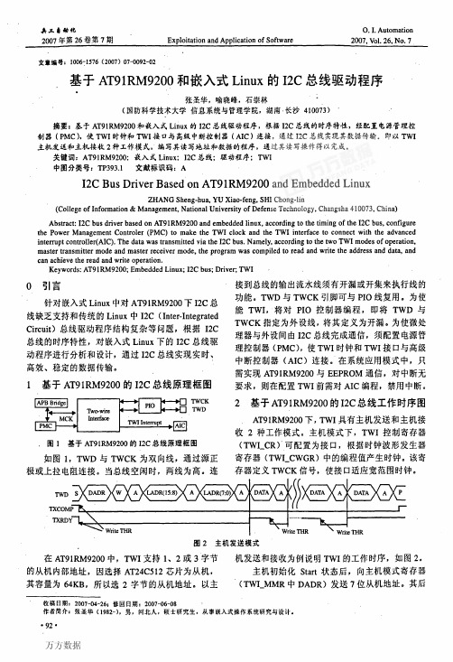
图2主机发送模式
.
在AT9lRM9200中,Twl支持l、2或3字节 机发送和接收为例说明TwI的工作时序,如图2。
的从机内部地址,因选择AT24C512芯片为从机,
2 基于AT91RM9200的12C总线工作时序图
AT91RM9200下,TwI具有主机发送和主机接 收2种工作模式。主机模式下,TwI控制寄存器
(TWLCR)。可配置为接口,根据时钟波形发生器
如图1,TwD与TWCK为双向线,通过源正 极或上拉电阻连接。当总线空闲时,两线为高。连
K’
z’\\wHtcTHR
【5】周剑波。基于FPGA和嵌入式Linux的网络视频采集处
理系统研究【D】.北京:北京科技大学,2Q06.
·93·
万方数据
主机初始化Start状态后,向主机模式寄存器
其容量为64KB,所以选2字节的从机地址。以主 ‘(TwI—MMR中DADR)发送7位从机地址。其后
收稿日期}2007—04—26l修回日期:2007一06一08 作者简介:张圣华(1982一),男,河北人,硕士研究生,从事嵌入式操作系统研究与设计. ·92·
动程序进行分析和设计,通过12C总线实现实时、 高效、稳定的数据传输。
僦脍 1 基于AT91RM9200的12C总线原理框图
I坐呈璺!g!I
—忑二=,
TWCK TWD
陌n:者薪习h
McK。 -
图1 基于AT91RM9200的12C总线原理框图
接到总线的输出流水线须有开漏或开集来执行线的 功能。TWD与TwCK引脚可与PIO线复用。为使 能TWI,将对PIO控制器编程,即将TwD与 TwcK指定为外设线,将其定义为开漏。为使微处 理器与外设间由12C总线完成通信,须配置电源管 理控制器(PMC),使TwI时钟和TwI接口与高级 中断控制器(AIC)连接。在系统应用模式中,只 需实现AT9lRM9200与EEPROM通信,对中断无 要求,则在配置TWI前需对AIC编程,禁用中断。
- 1、下载文档前请自行甄别文档内容的完整性,平台不提供额外的编辑、内容补充、找答案等附加服务。
- 2、"仅部分预览"的文档,不可在线预览部分如存在完整性等问题,可反馈申请退款(可完整预览的文档不适用该条件!)。
- 3、如文档侵犯您的权益,请联系客服反馈,我们会尽快为您处理(人工客服工作时间:9:00-18:30)。
的 以 太 网 控 制 芯 片 ) 另 一 种 是 通 过 以 ; 太 网接 E控 制 芯 片 ( L l 如 AN9 C 6 l 9 、RT 一 L
2 MA控制 送 出去 。 接 收 数据 帧 :首 先通 过 底层 芯片 将
‘ B R 、1 T C D )…. . 按迭字节 寄存器 D MA接收 寄存器 ( SAK …… 一 面起始 地址寄存 器 P T T) 页 ( S OP) PT …… …. 停止寄存 器 页面 ( UR C R)~……一 当前 页面寄存 器 ( NR B y)…… …一 界指针 寄存器 边 ( B …… ……. 收字节寄 存器 R C) 接
制器的以太网接口 驱动程序设计来系统地 J 【上 数据 帧的控制功能 提供 MI Me i 硐 I( d a 分析以太网控制器和物理 层芯片的驱动程 l Id p n e  ̄l efc )标准管理通信接 nee dn i r e n a
n。但它本身不具有直接 从网上收发数 据 的能力 必须接台物理层数据传输 1 A 9R 20 芯片 D 1 1 M9 6 来完成对网上数据的接 T1M90 以太网控制器及物 f 理层芯片 D 9 6 工作原理 M 11 『 收解码和 敖据帧编 码发送 任务 根据圈 1 ,可以看出 MAC层是通过 DMA 控制 方式来接手发送 和接收数据 , 1 1 A 1 M9 0 融控制器… . T9 R 20 DMA 直接通过 AS B总线与存储器进行通 A 1 M9 0是 由An 公 司针对通 f T9R 20 tml 信 。EMAc( 以太 r控制 器】 蝴 与物理 层芯 片 信 领 域 , 系 统 控 制 推 出 的 一 种 基 于
.
序设计原理和实现方法 。
A R M 9 0 2 T
前言
随着嵌人式 系统在 工程应 用和人们生 括中 的运用 越来越 广 .对它 的分析 研究 也越 来越 多 ,嵌入式 系统 与通信 、网络 技术的结合可以极大地增强网络的智能化 与灵 活性 ,拓展 通信功 能 ,从而实 现各
块即以太嗣控制器部分 ,由它集台物理层 恃输芯片 D 1 1 M9 6 殛相应的驱动程序来通 过 DMA控制方式完成对网上敖据帧的读
平台 L,针对相同的底屠芯片需要编辑 不 J 写 。 同的驱动程序s 而相同的操作系 统在不同 『 12 . 鼬太网接 口控制 器的 工作 原理
的硬件平 台上也需要编辑不同的驱动程序。
维普资讯
基于 AT 1 9 RM9 0 微控 制器的 20
以太 网接 口驱 动程序设 计
程 佳佳 宋 晓红 张宁 北 京 交通 大 学计算 机 网络 管 理 中 10 4 04 0
种通 信 系统 之 间的互 联互通 根据嵌人 式 内核可 裁减 、硬 件和驱动 程序 紧密结 合的特点 ,不 同的操 作系统 在同一 个硬件
图 3 以太 网控制器 D A通道数据传输原理 图 、 M
图 2 以太网控制器内部功 能模块 图 、
D MA发送寄 存器 ( P R) T s …… …~ 发送页面 起始寄存 器
之 间通 信是通过 P O口来实现。在实际的 I 驱 动程序 编写 中可 以通过 设置 PI 口的 O
P DR ( I ia l e i e )来 配 置 使 P O D sbe R gs r t
在编写躯动程序之前首先分析 一下它
而以太网通信接 口驱动程序通常是嵌入式
的硬件电路.以太网接 I部分主要分成两 1 : 系统所必需的 ,有时为 了各种原因 ,如安 l 个部分:”. 以太嗣控制器t )物理 层实现 . 2 全性或实时性等考虑需要更换其它操作系 『 数据帻的发送和接收芯片 统,选时原有的以太网驱动程序就不再有 AT 9 1 RM9 0 2 0本身带有 以太 研控 制 用,必须更改。本文就 A I, 2 0 T9PM9 0 撇控 1 器,兼容 I E 8 2 3 议标准 .具有对 E E 0 .
据帧的 MAC地 址 ,帧头信息和 C RC校 验 码 是 否正 确 ,如 果 不正 确 就 册 除 掉 , 0 正确通过 DMA 通道将数据拷 贝到接收缓
采用 RMI 还是 MI 控 制方式视硬件 I I 电路 设 计而 定 ,如今 大 多采 用 R I( 简 MI 精
。
存 区 。这 个过 程 涉及 到 复杂 的存 储 区管
维普资讯
C N l 吃 J = o T Ur K
=
ME啪 R Y
U ^
C
1 6 IBtI . I1 2y I} 1 } tFO ¨  ̄l 8  ̄
^
卜
D^ ^ T
S S TEM Y ∞ , H O
£ M oRY
2 1D . MA通 道数据传输控制原理
图 3描述 了数据 帧是 如何由 D MA通 道 来进 行数 据 传输 , 网上接 收到 的数 据 帧通过 D l l M9 6 解码后传输 到 F F I O,然
能 MDC ( 管理数据控制 器) ,MDI ( O 管
理数据输入输 出) E 0 ( , F1 0 使能全双工 10 0 M以太网)采用 MI R I , I MI / 方式选择等
1I 2
接收 到 的数 据 帧传输 到 28字节 的接 收 F F 中, IO 当一帧数据接收完以后 ,检验数
理 ,必 须结 合 了解存 储 区 之 间的关 系 。
型 MI)方 式 ,只 需 连 两 根 线 ( XD / , I R 0 1
图 4、D MA控 制器 中发送 、接收核 心寄存器
Tx / ) D0 1 ,简洁方便。
13 以太 网控 制 器 的 功 能 及 对 发 送 和 .
接收数据 帧的控制原理