SOD系列封装
sod123二极管参数

sod123二极管参数
SOD123型号是一种二极管封装类型,具体的二极管参数会根据具体的二极管型号而有所差异。
一般来说,SOD123封装的二极管参数包括以下几个方面:
1. 最大可反向电压(VRRM):表示二极管能够承受的最大反向电压,单位为伏特(V)。
2. 最大可持续反向电压(VR):表示二极管能够长时间承受的反向电压,单位为伏特(V)。
3. 最大正向电流(IF):表示二极管正向电流的最大值,单位为安培(A)。
4. 电压降(VF):表示二极管正向导通时的电压降,也称为正向压降,单位为伏特(V)。
5. 最大反向漏电流(IR):表示二极管在最大可反向电压下的反向漏电流,单位为安培(A)。
6. 瞬态热阻(RθJA):表示二极管的瞬态热阻,即在单位时间内从二极管到环境的热阻,单位为摄氏度/瓦特(℃/W)。
需要注意的是,具体的二极管型号会有不同的参数范围,可以根据具体的型号手册或数据表来获取详细的参数值。
SOD123封装500m系列稳压管

19.0
EA
25.65
27
28.35
50
0.01
20.4
EC
26.60
28
29.40
50
0.01
21.2
MMSZ4713
MMSZ4714 MMSZ4715
ED
28.50
30
31.50
50
0.01
22.8
EE
31.35
33
34.65
50
0.01
25.0
EF
34.20
36
37.80
50
0.01
27.3
MMSZ4716
1
1
10
100
VZ, NOMINAL ZENER VOLTAGE (V)
Figure 5 Effect of Zener Voltage on Zener Impedance
RATING AND CHARACTERISTICS CURVES ( MMSZ4681-MMSZ4717 )
C, CAPACITANCE (pF)
EH
37.05
39
40.95
50
0.01
29.6
MMSZ4717
EJ
40.85
43
45.15
50
0.01
32.6
Notes 1. Nominal Zener voltage is measured with the device junction in thermal equilibrium at TL = 30OC +1OC. 2. "Fully RoHS Compliant","100% Sn Plating (Pb-free)".
静电保护器SOD-882封装参数型号规格书大全

JEDEC SOD-882 Package Molding Compound Flammability Rating : UL 94V-O Quantity Per Reel : 1,0000pcs Reel Size : 7 inch Lead Finish : Lead Free Device Marking: P
Soldering Pad Layout Application Information
Dimensilimeters
1.30 0.75 0.20 0.55 0.80
Max. 0.53 0.05 0.55 1.075 0.675 0.45
Inches 0.051 0.029 0.007 0.021 0.031
SOD-882
Ultra Low Capacitance 0.5 pF Low Clamping Voltage Small Body Outline Dimensions:
0.039″ x 0.024″ (1.00 mm x 0.60 mm) Low Body Height: 0.020″ (0.5 mm) Stand−off Voltage: 3.3 V Low leakage current Response Time is Typically < 1.0 ns IEC61000−4−2 Level 4 ESD Protection This is a Pb−Free Device
SOD-723贴片二极管封装尺寸

【 南京南山半导体有限公司 — 长电三极管选型资料】
Symbol A A1 b c D E E1 E2 L θ
The top gasket Stamp “EMPTY” on the empty box Seal the box with the tape
Seal the box with the tape
QA Label
Label on the Inner Box Inner Box: 210 mm× 208mm× 203mm
Dimensions In Inches Min. Max. 0.021 0.026 0.020 0.023 0.010 0.014 0.003 0.006 0.022 0.026 0.035 0.043 0.051 0.059 0.008 REF. 0.001 0.003 7° REF.
【 南京南山半导体有限公司 — 长电三极管选型资料】
【 南京南山半导体有限公司 — 长电三极管选型资料】
【 南京南山半导体有限公司 — 长电三极管选型资料】
The bottom gasket
Label on the Reel 8000×15 PCS 8000×1 PCS
Label on the Outer Box
Outer Box: 440 mm× 440mm× 230mm
ห้องสมุดไป่ตู้
Dimensions In Millimeters Min. Max. 0.525 0.650 0.515 0.580 0.250 0.350 0.080 0.150 0.550 0.650 0.900 1.100 1.300 1.500 0.200 REF. 0.010 0.070 7° REF.
SOD882D:无铅封装产品
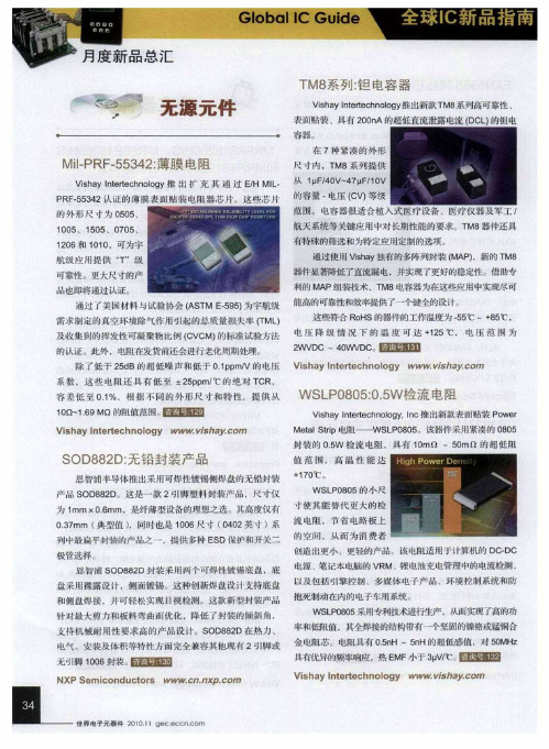
5H n 0 z 电气 、安装及体 积等特性方面完全兼容其他现有 2引脚或 盒电阻芯 电阻具有 0 n 一5 H的趣低感值,对 5 MH
无引脚 10 装 。 固圃 06封 暖圈
NXP S m ion u t r www.n n p c r e c d cos c .x .o n
具有 的频率 优异 响应. M 小 p/ 热E F 于3V ̄ 届圈■圜 C
2 V C一4WV C 目墨 圈 田 W D 0 D。
s n e t hn og v sh j n 除了低于 2d 5 B的 超 低 噪 声 和 低 于 01 p p mN 的 电 压 Vi hay I t rec ol y ww w. i a  ̄cor
系数 ,这些 电阻还具 有低 至 ±2 p m/ 的绝对 T 5p ℃ CR.
Gl ba Gude o lI I C i
品 总 汇
T 8 M 系列 : 电容器 钽
・
壬l沤 元 件 iL, _ i a4W 0 I i  ̄
Vs a tr c n l y lh yI et h oo 推出新款 T 系列高可靠性 、 n e g M8
表面贴装、具有 2 0 A的超低直流泄露 电流 ( CL 的钽电 0n D )
V s a t r e h ol g i h yI e t c n o y n _ vs a . o i h yc m
L … … … … … …
Hale Waihona Puke 容整 低至 0’ % 根据不 同的外 形尺 寸和特性 .提 供从
WS P 8 50 5 L 0 0 :.W检 流 电阻
Vs a n r c n lg ,n 推出新款表面贴装 P w r ih yIt t h o y Ic ee o o e M tl tp电阻——ws P 8 5 ea r Si L 0 0 该器件采用紧凄的 0 0 85 封装的 05 W检 流电阻. 具有 1 mn ~5 m ̄ 的超 低阻 0 0 !
安森美MMSZ系列齐纳二极管(SOD123封装)

MMSZ5221BT1 SeriesPreferred DeviceZener Voltage Regulators 500 mW SOD−123 Surface MountThree complete series of Zener diodes are offered in the convenient, surface mount plastic SOD−123 package. These devices provide a convenient alternative to the leadless 34−package style.Features•500 mW Rating on FR−4 or FR−5 Board•Wide Zener Reverse V oltage Range − 2.4 V to 110 V •Package Designed for Optimal Automated Board Assembly •Small Package Size for High Density Applications •General Purpose, Medium Current•ESD Rating of Class 3 (>16 kV) per Human Body Model •Pb−Free Packages are AvailableMechanical Characteristics:CASE:V oid-free, transfer-molded, thermosetting plastic case FINISH:Corrosion resistant finish, easily solderableMAXIMUM CASE TEMPERATURE FOR SOLDERING PURPOSES: 260°C for 10 SecondsPOLARITY:Cathode indicated by polarity band FLAMMABILITY RATING:UL 94 V−0MAXIMUM RATINGSRating Symbol Max UnitTotal Power Dissipation on FR−5 Board, (Note 1) @ T L = 75°CDerated above 75°C P D5006.7mWmW/°CThermal Resistance, Junction−to−Ambient(Note 2)R q JA340°C/WThermal Resistance, Junction−to−Lead(Note 2)R q JL150°C/W Junction and Storage Temperature Range T J, T stg−55 to +150°CMaximum ratings are those values beyond which device damage can occur. Maximum ratings applied to the device are individual stress limit values (not normal operating conditions) and are not valid simultaneously. If these limits are exceeded, device functional operation is not implied, damage may occur and reliability may be affected.1.FR−5 = 3.5 X 1.5 inches, using the minimum recommended footprint.2.Thermal Resistance measurement obtained via infrared Scan Method.See specific marking information in the device marking column of the Electrical Characteristics table on page 3 of this data sheet.DEVICE MARKING INFORMATIONDevices listed in bold, italic are ON Semiconductor Preferred devices. Preferred devices are recommended choices for future use and best overall value.ELECTRICAL CHARACTERISTICS (T A = 25°C unless otherwise noted, V F = 0.95 V Max. @ I F = 10 mA)Symbol ParameterV Z Reverse Zener Voltage @ I ZTI ZTReverse CurrentZ ZT Maximum Zener Impedance @ I ZTI ZK Reverse CurrentZ ZK Maximum Zener Impedance @ I ZKI R Reverse Leakage Current @ V RV R Reverse VoltageI F Forward CurrentV F Forward Voltage @ I F/ONELECTRICAL CHARACTERISTICS (T A = 25°C unless otherwise noted, V F = 0.9 V Max. @ I F = 10 mA)DeviceDeviceMarkingZener Voltage (Notes 3 and 4)Zener Impedance (Note 5)Leakage Current V Z (Volts)@ I ZT Z ZT @ I ZT Z ZK @ I ZK I R @ V R Min Nom Max mA W W mA m A VoltsMMSZ5221BT1, G C1 2.28 2.4 2.52203012000.251001 MMSZ5222BT1, G C2 2.38 2.5 2.63203012500.251001 MMSZ5223BT1, G C3 2.57 2.7 2.84203013000.25751 MMSZ5224BT1, G C4 2.66 2.8 2.94203014000.25751 MMSZ5225BT1, G C5 2.85 3.0 3.152********.25501 MMSZ5226BT1, G D1 3.14 3.3 3.47202816000.25251 MMSZ5227BT1, G D2 3.42 3.6 3.78202417000.25151 MMSZ5228BT1, G D3 3.71 3.9 4.10202319000.25101 MMSZ5229BT1, G D4 4.09 4.3 4.52202220000.2551 MMSZ5230BT1, G D5 4.47 4.7 4.94201919000.2552 MMSZ5231BT1, G E1 4.85 5.1 5.36201716000.2552 MMSZ5232BT1, G E2 5.32 5.6 5.88201116000.2553 MMSZ5233BT1, G E3 5.70 6.0 6.3020716000.255 3.5 MMSZ5234BT1, G E4 5.89 6.2 6.5120710000.2554 MMSZ5235BT1, G E5 6.46 6.87.142057500.2535 MMSZ5236BT1, G F17.137.57.882065000.2536 MMSZ5237BT1, G F27.798.28.612085000.253 6.5 MMSZ5238BT1, G F38.278.79.142086000.253 6.5 MMSZ5239BT1, G F48.659.19.5620106000.2537 MMSZ5240BT1, G F59.501010.5020176000.2538 MMSZ5241BT1, G H110.451111.5520226000.2528.4 MMSZ5242BT1, G H211.401212.6020306000.2519.1 MMSZ5243BT1, G H312.351313.659.5136000.250.59.9 MMSZ5244BT1, G H413.301414.709.0156000.250.110 MMSZ5245BT1, G H514.251515.758.5166000.250.111 MMSZ5246BT1, G J115.201616.807.8176000.250.112 MMSZ5247BT1, G J216.151717.857.4196000.250.113 MMSZ5248BT1, G J317.101818.907.0216000.250.114 MMSZ5250BT1, G J519.002021.00 6.2256000.250.115 MMSZ5251BT1, G K120.902223.10 5.6296000.250.117 MMSZ5252BT1, G K222.802425.20 5.2336000.250.118 MMSZ5253BT1, G K323.752526.25 5.0356000.250.119 MMSZ5254BT1, G K425.652728.35 4.6416000.250.121 MMSZ5255BT1, G K526.602829.40 4.5446000.250.121 MMSZ5256BT1, G M128.503031.50 4.2496000.250.123 MMSZ5257BT1, G M231.353334.65 3.8587000.250.125 MMSZ5258BT1, G M334.203637.80 3.4707000.250.127 MMSZ5259BT1, G M437.053940.95 3.2808000.250.130 MMSZ5260BT1, G M540.854345.15 3.0939000.250.133 MMSZ5261BT1, G N144.654749.35 2.710510000.250.136 MMSZ5262BT1, G N248.455153.55 2.512511000.250.139 MMSZ5263BT1, G N353.205658.80 2.215013000.250.143 MMSZ5264BT1, G N457.006063.00 2.117014000.250.146 MMSZ5265BT1, G N558.906265.10 2.018514000.250.147 MMSZ5266BT1, G P164.606871.40 1.823016000.250.152 MMSZ5267BT1, G P271.257578.75 1.727017000.250.156 MMSZ5268BT1, G P377.908286.10 1.533020000.250.162 MMSZ5269BT1P482.658791.35 1.437022000.250.168 MMSZ5270BT1, G P586.459195.55 1.440023000.250.169 MMSZ5272BT1, G R2104.5110115.5 1.175030000.250.1843.The type numbers shown have a standard tolerance of ±5% on the nominal Zener voltage.4.Nominal Zener voltage is measured with the device junction in thermal equilibrium at T L = 30°C $1°C.5.Z ZT and Z ZK are measured by dividing the AC voltage drop across the device by the ac current applied.The specified limits are for I Z(AC) = 0.1 I Z(dc) with the AC frequency = 1 KHz.*The “G’’ suffix indicates Pb−Free package available./ONV Z , NOMINAL ZENER VOLTAGE (V)−1012345678Figure 1. Temperature Coefficients (Temperature Range −55°C to +150°C)100101V Z , NOMINAL ZENER VOLTAGE (V)Figure 2. Temperature Coefficients (Temperature Range −55°C to +150°C)1.21.00.80.60.40.20T, TEMPERATURE (°C)Figure 3. Steady State Power Derating PW, PULSE WIDTH (ms)Figure 4. Maximum Nonrepetitive Surge Power1000100101V Z , NOMINAL ZENER VOLTAGEFigure 5. Effect of Zener Voltage onZener Impedance1000100101V F , FORWARD VOLTAGE (V)Figure 6. Typical Forward Voltageq V Z , T E M P E R A T U R E C O E F F I C I E N T (m V /°C )q V Z , T E M P E R A T U R E C O E F F I C I E N T (m V /°C )P p k , P E A K S U R G E P O W E R (W A T T S )Z Z T , D Y N A M I C I M P E D A N C E (W )C , C A P A C I T A N C E (p F )1000100101V Z , ZENER VOLTAGE (V)1001010.10.01V Z , ZENER VOLTAGE (V)1001010.10.01V Z , NOMINAL ZENER VOLTAGE (V)Figure 8. Typical Leakage CurrentFigure 9. Zener Voltage versus Zener Current(V Z Up to 12 V)Figure 10. Zener Voltage versus Zener Current(12 V to 91 V)I R , L E A K A G E C U R R E N T (m A )I Z , Z E N E R C U R R E N T (m A )I Z , Z E N E R C U R R E N T (m A )PACKAGE DIMENSIONSSOD−123CASE 425−04ISSUE Eǒmm inchesǓSCALE 10:1*For additional information on our Pb−Free strategy and solderingdetails, please download the ON Semiconductor Soldering and Mounting Techniques Reference Manual, SOLDERRM/D.SOLDERING FOOTPRINT*ON Semiconductor and are registered trademarks of Semiconductor Components Industries, LLC (SCILLC). SCILLC reserves the right to make changes without further notice to any products herein. SCILLC makes no warranty, representation or guarantee regarding the suitability of its products for any particular purpose, nor does SCILLC assume any liability arising out of the application or use of any product or circuit, and specifically disclaims any and all liability, including without limitation special, consequential or incidental damages.“Typical” parameters which may be provided in SCILLC data sheets and/or specifications can and do vary in different applications and actual performance may vary over time. All operating parameters, including “Typicals” must be validated for each customer application by customer’s technical experts. SCILLC does not convey any license under its patent rights nor the rights of others. SCILLC products are not designed, intended, or authorized for use as components in systems intended for surgical implant into the body, or other applications intended to support or sustain life, or for any other application in which the failure of the SCILLC product could create a situation where personal injury or death may occur. Should Buyer purchase or use SCILLC products for any such unintended or unauthorized application, Buyer shall indemnify and hold SCILLC and its officers, employees, subsidiaries, affiliates,and distributors harmless against all claims, costs, damages, and expenses, and reasonable attorney fees arising out of, directly or indirectly, any claim of personal injury or death associated with such unintended or unauthorized use, even if such claim alleges that SCILLC was negligent regarding the design or manufacture of the part. SCILLC is an Equal Opportunity/Affirmative Action Employer. This literature is subject to all applicable copyright laws and is not for resale in any manner.PUBLICATION ORDERING INFORMATION。
SOD-523贴片二极管封装尺寸对照表

【 南京南山半导体有限公司 — 长电三极管选型资料】
【 南京南山半导体有限公司 — 长电三极管选型资料】
【 南京南山半导体有限公司 — 长电三极管选型资料】
The bottom gasket
Label on the Reel 8000×15 PCS 8000×1 PCS
The top gasket Stamp “EMPTY” on the empty box Seal the box with the tape
Seal the box with the tape
QA Label
Label on the Inner Box Inner Box: 210 mm× 208mm× 203mm
Dimensions In Millimeters Min Max 0.510 0.770 0.500 0.700 0.250 0.350 0.080 0.150 0.750 0.850 1.100 1.300 1.500 1.700 0.200 REF 0.010 0.070 7° REF
Dimensions In Inches Min Max 0.020 0.031 0.020 0.028 0.010 0.014 0.003 0.006 0.030 0.033 0.043 0.051 0.059 0.067 0.008 REF 0.001 0.003 7° REF
sod523贴片二极管封装尺寸对照表贴片二极管封装贴片二极管封装尺寸贴片二极管封装规格贴片二极管封装大全贴片发光二极管封装贴片稳压二极管封装贴片肖特基二极管封装贴片二极管m7封装贴片4148二极管封装
【 南京南山半导体有限公司 — 长电三极管选型资料】
Symbol A A1 b c D E E1 E2 L θ
SOD-523贴片二极管封装尺寸对照表
Outer Box: 440 mm× 440mm× 230mm
【 南京南山半导体有限公司 — 长电三极管选型资料】
【 南京南山半导体有限公司 — 长电三极管选型资料】
【 南京南山半导体有限公司 — 长电三极管选型资料】
The bottom gasket
Label on the Reel 8000×15 PCS 8000×1 PCS
sod523贴片二极管封装尺寸贴片二极管封装尺寸贴片发光二极管封装二极管贴片封装贴片电阻封装尺寸贴片封装尺寸in4148贴片封装尺寸贴片电阻封装尺寸图tlp521贴片封装尺寸sod123封装尺寸
【 南京南山半导体有限公司 — 长电三极管选型资料】
Symbol A A1 b c D E E1 E2 L θ
The top gasket Stamp “EMPTY” on the empty box Seal the box with the tape
Seal the box with the tape
QA Label
Label on the Inner Box Inner Box: 210 mm× 208mm× 203mm
Dimensions In Millimeters Min Max 0.510 0.770 0.500 0.700 0.250 0.350 0.080 0.150 0.750 0.850 1.100 1.300 1.500 1.700 0.200 REF 0.010 0.070 7° REF
Dimensions In Inches Min Max 0.020 0.031 0.020 0.028 0.010 0.014 0.003 0.006 0.030 0.033 0.043 0.051 0.059 0.067 0.008 REF 0.001 0.003 7° REF