TSCDA14中文资料
SCD工具使用

➢每个SMV访问点参数中,只需按工程需要,修改 MAC-Address、VLAN-ID、VLAN-PRIORITY、 APPID,其余参数保持工具默认值即可;
制作SCD-SMV通讯子网设置
➢MAC-Address:SMV组播地址,全站唯一,有效 范围为01-0C-CD-04-00-00~01-0C-CD-04-01FF;
配置IED - GSE Control 选项
配置IED - SMV Control 选项
➢ 此项仅对9-2采样值传输有效,用于配置SMV发送数据集对应的 控制块。一般选择合并单元装置,选择GOOSE的LD,在右侧窗口 可添加SMV发送控制块,除data set需选择,其余参数保留不变。
➢ Name:LD内唯一,一般取默认值; ➢ DataSet:选择GOOSE LD下的SMV数据集,每个数据集对应一个
SCD工具结构-Header部分
➢ 记录SCD文件的更新记录
SCD工具结构-Communication部分
➢现场实际物理通讯子网的映射 ➢MMS独立组网时,子网的类型为8-MMS,子网的
address中存放本子网内装置的MMS访问点; ➢GOOSE独立组网时,子网的类型为IECGOOSE,子
网的GSE中存放本子网内装置的GOOSE访问点; ➢SV独立组网时,子网的类型为SMV,子网的SMV
➢SCD运行目录下,BIN目录为运行程序目录, SCLConfigurator.exe为SCD组态程序,ICD目录 为需要导入的ICD存放目录,CID目录为单独导 出的CID文件所在目录,Export为导出CID及 GOOSE的目录,SCD为存放SCD文件的目录,SSD 为存放SSD文件的目录。
扫描特ktronic规格标准及合规性说明书

ScantronicSpecificationsStandards and ComplianceThe installer must remove or adjust any compliance labelling if a non-compliant configuration is selected.Intrusion compliance : EN 50131-1:2007+A2:2017; EN 50131-3:2009; EN 50131-6:2017+A1:2021; EN 50131-10:2014; EN 50136-2:2013; BS8243:2010; PD6662:2017Security grade : Grade 2.Environmental class : Class II.Protection: IP40, IK06.SecurityAccess codes : 4-digit, giving 10,000 combinations. 6-digit, giving 1,000,000 combinations.Code blocking : Blocked for 90 secs after 4 incorrect codes in series.Proximity tag differs : 4,294,967,296.GeneralRelative Humidity : 0 to 93%, non-condensing.Operating temp. range : -10°C to +55°C.Dimensions : 239mm (h) x 250mm (w) x 87mm (d).Weight : 2.8kg (without battery).Case material : Steel.ElectricalThis product complies with the requirements of EN50131-6 Type A power supply at Grade 2 and environmental class II.Mains power supply : 230Vac + 10%/-15%, 200mA max, 50Hz.Control unit internal mains fuse : T250mA.Control unit power supply : 13.7Vdc, 1.0A max of which 180mA is reserved for battery recharge and 820mA to power the system.Control unit PCB current consumption : 40mA quiescent; 70mA max (in alarm) excluding external devices and battery charging.Standby battery : 12V, 7Ah, sealed lead acid. Min standby time:12 hrs. (see “Step 2: Check standby battery capacity”). Max recharge time: 72 hrs.12V aux : 600mA max*12V bus : 400mA max*12V to plug-by communicator : 400mA max**Maximum current before triggering over-current protection. Output voltage range : 12V outputs are 9.5Vdc to 13.8Vdc. Max p-to-p ripple voltage : 0.5V.Low-battery fault at : <12V.Aux power output fault at : <9V.OP1-3: Open collector transistor, 500mA max.Plug-by outputs : Open collector transistor, 50mA max.Loudspeaker : 12Vdc, 280mA max. Min impedance 16 Ohm.The information, recommendations, descriptions and safety notations in this document are based on Eaton Corporation’s (“Eaton”) experience and judgment and may not cover all contingencies. If further information is required, an Eaton sales office should be consulted. Sale of the product shown in this literature is subject to the terms and conditions outlined in appropriate Eaton selling policies or other contractual agreement between Eaton and the purchaser.THERE ARE NO UNDERSTANDINGS, AGREEMENTS, WARRANTIES, EXPRESSED OR IMPLIED, INCLUDING WARRANTIES OF FITNESS FOR A PARTICULAR PURPOSE OR MERCHANTABILITY , OTHER THAN THOSE SPECIFICALL Y SET OUT IN ANY EXISTING CONTRACT BETWEEN THE PARTIES. ANY SUCH CONTRACT STATES THE ENTIREOBLIGATION OF EATON. THE CONTENTS OF THIS DOCUMENT SHALL NOT BECOME PART OF OR MODIFY ANY CONTRACT BETWEEN THE PARTIES.In no event will Eaton be responsible to the purchaser or user in contract, in tort (including negligence), strict liability or other-wise for any special, indirect, incidental or consequential damage or loss whatsoever, including but not limited to damage or loss of use of equipment, plant or power system, cost of capital, loss of power, additional expenses in the use of existing power facilities, or claims against the purchaser or user by its customers resulting from the use of the information, recommendations and descriptions contained herein. The information contained in this manual is subject to change without notice.© 2022 EatonEaton, Security House, Vantage Point Business Village, Mitcheldean, GL17 0SZ. Product Support (UK) Tel: +44 (0) 1594 541978 available 08:30 to 17:00 Monday to Friday. email:*****************************Installation InstructionsThe i-on10 is a 10-zone grade-2-compliant control unit. The i-on10 provides a reliable, easy-to-install, wired solution for domestic and small commercial applications.Key features•Supports up to 10 wired zones, all provided on-board.•Compatible with a range of wired detectors, including PIR sensors and door contacts. •Supports up to four keypads connected to the system bus. •Grade 2 compliant.•Support for one full-set level and up to three part-set levels. •Configurable through a keypad.•On-board connections for wired siren/strobe unit.•On-board open-collector output to operate an external auxiliary device. •Plug-by communicator port with 8 outputs to communicate with an alarms-receiving centre (requires MISC-COMPACK12 and a suitable standalone communicator, such as 0840UK-21). •Metal case, fitted with a 1A power supply and space for a 12Vdc 7Ah backup battery. •Back and lid tamper switches. •Support for up to 10 users.Safety InformationThis product must be installed by qualified service personnel. WARNING: BEFORE INSTALLING THIS EQUIPMENT , ENSURE THAT THE MAINS SUPPL Y FOR THE CONTROL UNIT IS DISCONNECTED AND ISOLATED. All electrical connections must be carried out by a qualified electrician and comply with current local regulations.WARNING : When connected to the mains with power applied, mains voltages are present on the shrouded heads of the terminal screws of the mains connector (Figure 4).WARNING: The mains cable to the control unit must use a double-pole isolation device in accordance with EN 62368-1.WARNING: Good practice requires that documentation is not stored within the enclosure.Caution: If you need to handle the PCB in the control unit, take standard precautions to prevent damage by static electricity.Installing the control unitStep 1: Choose a location for the control unitThe control unit must be located:•Within the protected area (but not in an entry or exit zone). •Out of sight of potential intruders.•Upright (battery at the bottom) on a wall or other flat surface (to discourage tamper attempts from the rear).Step 2: Check standby battery capacityCheck that the battery is able to power the system for at least 12 hours during a mains failure, including two periods of 15 minutes in alarm. This is the minimum period for grade 2 compliance.To do this, you will need to calculate the total current drawnfrom the battery during a mains failure. Please refer to the i-on10 Configuration Guide for worked examples.Step 3: Install cablingNote the following (refer to the i-on10 Configuration Guide for guidance):•Normally, standard 7/0.2 un-screened alarm cable is suitable for wiring to keypads and wired siren/strobe units. •Screened cable may be needed if the cable runs near to sources of electromagnetic interference. •Keep cables to keypads separate from any other wiring. •You can connect keypads using a daisy-chain (serial) or star (parallel) configuration. •Cables must enter the control unit using the dedicated cable-entry holes (Figure 1). •The maximum length of the cable to keypads depends on anumber of factors, including the number of keypads and whether daisy-chain or star connections are used.Step 4: Remove the lid of the control unitRelease the two screws on the front of the lid, then lift it off.Step 5: Mount the control unitMount the control unit in the orientation shown in Figure 1 using the three fixing holes and minimum 40mm long No8 (4mm) screws. Use only the designated cable-entry holes.entryMains Signal cable entryFigure 1. Fixing holes and cable entriesPart number 14199588Issue 2 24/01/22Step 6: Position the communicator and fit the fourth pillarIf a communicator is used, position it under the PCB.Fit the supplied fourth pillar for the PCB (see Figure 2), and securethe PCB to the pillar using the supplied M3x12 screw.Figure 2. Fitting the fourth pillarStep 7: Connect all wired devicesConnect all wired devices except the battery, as shown in Figure 3.Step 8: Connect the batteryNote: Connecting the battery does not start the system.Fit a 7Ah lead-acid battery in the bottom-left corner of the control unit.Connect the battery leads to the battery (red to positive and black to negative), and connect the transformer lead to the PCB (Figure 3).Step 9: Connect the mains cableENSURE THAT THE MAINS Y IS DISCONNECTED AND Figure 4. Mains connectionsStep 10: Re-fit the lid, switch on and configure the systemWARNING: During initial power-up, keypad sounders and anyinternal loudspeaker may give an alarm tone. If you are working at the top of a ladder, make sure that the sudden noise does not startle you and cause a fall.Re-fit the lid, then switch on the mains supply to the control unit.Go through the initial configuration prompts and set up the system as described in the i-on10 Configuration Guide . You are prompted to specify installer and user codes during initial system configuration.PCB links and connectorsThe following sections provide information about the links and connectors shown in Figure 3.a Plug-by communicator portYou can connect a plug-by communicator to this port using an optional MISC-COMPACK12 wiring harness (available separately). By default, outputs 1-8 are 0V when active, and 12Vdc when inactive. Please refer to the i-on10 Configuration Guide for the default output type used for each output and programming details.Connect LF (Line Fail) to an output from the communicator that is 12Vdc when communicator detects that there is a communications fault to the ARC, and 0V when no fault is present.If a dual-path (landline and mobile) communicator is used, such as a RedCARE STU, re-program one of the plug-by outputs to type ATS Test, and wire that to the ATS Test input of the communicator. Also connect Line Fail to the Line Fail output of the communicator, asabove. This is needed to comply with BSIA Form No. 175, April 2005. The control unit generates an “ATE LF Single” alert if one network is unavailable, or “ATE LF All” if both are unavailable.Connect RR (Remote Reset) to an output from the communicator that indicates to the control unit that a user can reset the system after a system tamper. The input must be 12Vdc for at least 100ms to indicate the reset, and 0v normally. For further details, see “Remote Reset (Redcare Reset)” in the i-on10 Configuration Guide .Note: During system commissioning, confirm with the ARC that the communicator is working correctly.b System busUp to four keypads can connect to the system bus. The installation instructions supplied with each keypad provide details of how to install the device. The address of each device is set by the control unit, as described in the i-on10 Configuration Guide .Please refer to “Step 3: Install cabling” for guidance about cabling.See also “RS485 bus termination link”.c Loudspeaker connectionsIf fitted, a loudspeaker mimics alarm tones and repeats setting and entry tones. The loudspeaker must be a minimum of 16 Ohms. Note:• A loudspeaker is not a warning device as described by EN50131-4. •You can set the loudspeaker volume from the Installer menu.d Open-collector (wired) outputThe open-collector transistor output can be used to switch external equipment on or off. By default, the output is 12Vdc when inactive and 0V when active (this can be reversed from the Installer menu).e Siren/strobe connectionsPlease refer to the installation instructions provided with the siren/strobe unit for connection details.f Wired zone connectionsYou can connect up to 10 wired detectors (0 to 9) to the control unit using the Fully-Supervised Loop (FSL), 4-wire Closed Circuit (CC) or 2-wire CC wiring method (Figure 5). You must use the same method for all detectors. If 4-wire CC is used, the number of zones is halved and are numbered 1-5. To maintain ten 4-wire CC zones (0-9), fit an ADP -10CC board and configure the resistance setting of each zone as 2k2/4k7.For any method, the total wiring and switch resistance must be lessthan 100 Ohms (EOL resistor shorted in the case of FSL).By default, the system assumes normally-closed contacts. Detectors with normally-open contacts must be programmed with the “Inverted” attribute set.Please refer to the i-on10 Configuration Guide for wiring details ifyou want to use two detectors per zone.Zone 0Zone 14-Wire CC Wiring2-Wire CC Wiring Supported resistor values (± 5%):EOL Alarm2k2 4k7 (default)1k0 1k02k2 2k24k7 4k7FSL Wiring, with 8k2 resistorsFigure 5. Zone wiringg Kick-start linkOrdinarily, the control unit starts only after the mains supply is switched on, even if a battery is connected. If you want to operate the control unit temporarily using only the battery, start the control unit by briefly shorting this link.h Reset codes linkYou can use this link to reset the installer and all user codes (e.g.in the event that codes have been forgotten). All proximity tags are also deleted. This link can be enabled or disabled by a setting in the Installer menu. Please refer to the i-on10 Configuration Guide for further details.i RS485 bus termination linkIf the control unit uses a single daisy chain to connect keypads and is at one end of the chain, fit a jumper across this link in the control unit and in the last keypad on the bus. RS485 termination canimprove performance in electrically noisy environments. The i-on10 Configuration Guide gives further guidance.MaintenanceInspect the control unit once or twice per year as part of general inspection of the whole system. At the control panel, check for any damage, test the battery, and check the action of the tamper switch.Please refer to the i-on10 Configuration Guide for general guidance about maintaining the whole system.Figure 3. Control unit PCBAB+120If a siren/strobe unit is not fitted, connect TR to 0V.d Open-collector outputb Ststem bus(Max 4 keypads)Connect transformer。
(整理)TouchKit四线产品规格书.
精品文档
精品文档
文件编号: 发行版本:4.0
SET
产品标准规格书 (线性式)
信赖性试验
发行日期:20010501 修定日期:20050501
页 次:06
精品文档
精品文档
6、信赖性试验
(1)高温测试 放置于 60℃之环境中,测试 72hr,取出室温放置 2 小时测,需满足 下列条件:
▲导通阻抗
300Ω ≤X≤900Ω 300Ω ≤X≤900Ω
面,需满足下列条件: ▲导通阻抗 300Ω ≤X≤900Ω 300Ω ≤X≤900Ω ▲绝缘阻抗 20MΩ ↑ @ DC25V ▲外型
TOUCHPANEL 上版 PET、下板玻璃不得有破裂情形发生。
(6) 击打测试
用击打测试仪,(笔尖 0.8mm2 打键荷重 110 克力,打键速度 2 次/秒)连续 100 万次以上,需满足下列条件:
>3H
100 万次以上(笔尖 0.8mm2 打键荷重 110 克力,打键速度 2
次/秒)
>80%
<1.5%
精品文档
精品文档
文件编号: 发行版本:4.0
SET 3、结构图
产品标准规格书 (线性式) 产品结构
发行日期:20010501 修定日期:20050501 页 次:03
项目 A B C D E F I G H
▲导通阻抗 300Ω ≤X≤900Ω 300Ω ≤X≤900Ω ▲绝缘阻抗 20MΩ ↑ @ DC25V
精品文档
精品文档
文件编号:
发行版本:4.0
SET
7、外观检验规范 (1)检验条件:
a、光源:40W 光管 b、距离,如图:
光管
产品标准规格书 (线性式)
1915042中文资料

Extract from the onlinecatalogEMSTBVA 2,5/20-GOrder No.: 1915042The figure shows a 10-position version of the producthttp://eshop.phoenixcontact.de/phoenix/treeViewClick.do?UID=1915042Header, nominal current: 12 A, rated voltage: 200 V, pitch: 5.0 mm, no. of positions: 20, mounting: press inhttp://Please note that the data givenhere has been taken from theonline catalog. For comprehensiveinformation and data, please referto the user documentation. TheGeneral Terms and Conditions ofUse apply to Internet downloads. Technical dataDimensions / positionsPitch 5 mmDimension a95 mmNumber of positions20Pin dimensions1,7 mmHole diameter 1.75 mmTechnical dataInsulating material group IIIaRated surge voltage (III/3) 4 kVRated surge voltage (III/2) 4 kVRated surge voltage (II/2) 4 kVRated voltage (III/2)320 VRated voltage (II/2)320 VConnection in acc. with standard EN-VDENominal current I N12 ANominal voltage U N200 VMaximum load current12 AInsulating material PBTInflammability class acc. to UL 94V0Certificates / ApprovalsApproval logoCULNominal voltage U N300 VNominal current I N10 AULNominal voltage U N300 VNominal current I N10 ACertification CB, CUL, GOST, UL, VDE-PZIAccessoriesItem Designation DescriptionAssembly1877203EMSTB 2,5-SH Stamp holder, for upper and lower stamp1877229EMSTBVA 2,5-SS-2-5,08Stamp set, consisting of an upper and lower stamp, upper stamp:17 to 24-pos., lower stamp: 2 to 24-pos., pitch: 5.08 mm 1755477MSTB-BL Keying cap, for forming sections, plugs onto header pin, greeninsulating materialMarking0804183SK 5/3,8:FORTL.ZAHLEN Marker card, printed horizontally, self-adhesive, 12 identicaldecades marked 1-10, 11-20 etc. up to 91-(99)100, sufficient for120 terminal blocksPlug/Adapter1734401CR-MSTB Coding section, inserted into the recess in the header or theinverted plug, red insulating materialAdditional productsItem Designation DescriptionAssembly1909391FKCT 2,5/20-ST Plug component, nominal current: 12 A, rated voltage: 250 V,pitch: 5.0 mm, no. of positions: 20, type of connection: Spring-cage connectionGeneral1779592FRONT-MSTB 2,5/20-ST Plug component, nominal current: 12 A, rated voltage: 250 V,pitch: 5.0 mm, no. of positions: 20, type of connection: Screwconnection1754805MSTB 2,5/20-ST Plug component, nominal current: 12 A, rated voltage: 250 V,pitch: 5.0 mm, no. of positions: 20, type of connection: Screwconnection1765959MSTBP 2,5/20-ST Plug component, nominal current: 12 A, rated voltage: 250 V,pitch: 5.0 mm, no. of positions: 20, type of connection: Screwconnection1792197MVSTBR 2,5/20-ST Plug component, nominal current: 12 A, rated voltage: 250 V,pitch: 5.0 mm, no. of positions: 20, type of connection: Screwconnection1792702MVSTBW 2,5/20-ST Plug component, nominal current: 12 A, rated voltage: 250 V,pitch: 5.0 mm, no. of positions: 20, type of connection: Screwconnection1768930SMSTB 2,5/20-ST Plug component, nominal current: 12 A, rated voltage: 250 V,pitch: 5.0 mm, no. of positions: 20, type of connection: ScrewconnectionDrawingsDrilling diagramDimensioned drawingAddressPHOENIX CONTACT GmbH & Co. KGFlachsmarktstr. 832825 Blomberg,GermanyPhone +49 5235 3 00Fax +49 5235 3 41200http://www.phoenixcontact.de© 2008 Phoenix ContactTechnical modifications reserved;。
TSC工业级打印机使用手册
3.1 Setup (設定) ............................................................................................ 35 3.1.1-1 Print Setup (列印設定/TSPL2)................................................... 36 3.1.1-2 Printer Setup (列印設定/ZPL2) .................................................. 43 3.1.2 Sensor (感應器設定) ..................................................................... 49 3.1.3 Serial Comm. (串列埠設定)........................................................... 57 3.1.4 Ethernet (乙太網路設定) ............................................................... 60 3.2 File Manager (檔案管理) ......................................................................... 63 3.2.1 File List (檔案清單)........................................................................ 63 3.2.2 Avail. Memory (可用記憶體) ......................................................... 64 3.2.3 Del. All Files (刪除檔案) ................................................................ 64 3.3 Diagnostics (印表機診斷) ....................................................................... 65 3.3.1 Print Config. (列印設定組態) ........................................................ 65 3.3.2 Dump Mode (除錯模式)................................................................. 66 3.3.3 Rotate Cutter (旋轉裁刀) .............................................................. 67 3.4 Language (語言) ..................................................................................... 67 3.5 Service (服務) ......................................................................................... 68 3.5.1 Initialization (印表機預設值) ......................................................... 68 3.5.2 Mileage Info. (里程資訊) ............................................................... 69 4. 印表機診斷工具(Diagnostic Tool) ............................ 70 4.1 啟用 Diagnostic Tool 工具程式 .............................................................. 70 4.2 印表機組態設定 (感應器校正、設定乙太網路、設定印表機 RTC 時間參 數…..) ............................................................................................................ 71 5. 用印表機診斷工具(Diagnostic Tool)設定乙太網路(TTP-246M Pro/TTP-344M Pro 機種此為選配功能) ......................................................... 72 5.1 經由 USB 介面設定 .................................................................................. 72 5.2 經由 RS-232 介面設定 ............................................................................. 73 5.3 經由 Ethernet 介面設定 .......................................................................... 74 6. 故障排除 .............................................. 76 6.1 常見問題 .................................................................................................. 76 6.2 皺摺解說及排除 ........................................................................................ 80 7. 印表機簡易保養 ......................................... 82 警示:安全指示說明 ........................................ 83 更新記錄 ................................................ 84
四川省农业厅关于发布《2014年四川省农业机械推广鉴定产品种类指

四川省农业厅关于发布《2014年四川省农业机械推广鉴定产品种类指南》及《2014年四川省农业机械推广鉴定大纲目
录》的公告
【法规类别】农业科技与农机
【发文字号】川农业函[2014]74号
【发布部门】四川省农业厅
【发布日期】2014.03.19
【实施日期】2014.03.19
【时效性】现行有效
【效力级别】XP10
四川省农业厅关于发布《2014年四川省农业机械推广鉴定产品种类指南》及《2014年四
川省农业机械推广鉴定大纲目录》的公告
(川农业函[2014]74号)
根据《农业机械试验鉴定办法》(农业部令第54号)的规定,我厅制定了《2014年四川省农业机械推广鉴定产品种类指南》及《2014年四川省农业机械推广鉴定大纲目录》,现予发布。
特此公告。
附件:1、2014年四川省农业机械推广鉴定产品种类指南
2、2014年四川省农业机械推广鉴定大纲目录
四川省农业厅
2014年3月19日
附件1:
2014年四川省农业机械推广鉴定产品种类指南。
TSC2046EVM-PDK;TSC2046EVM;中文规格书,Datasheet资料

User's GuideSBAU100–September2004This user's guide describes the characteristics,operation,and use of theTSC2046EVM,both by itself and as part of the TSC2046EVM-PDK.This EVM is a4-wire touch screen controller evaluation module which also has auxiliary inputs andbattery and temperature measurement capabilities.A complete circuit description,schematic diagram,and bill of materials are included.documents are available through the Texas Instruments web siteatEVM-Compatible Device Data SheetsContents1EVM Overview (2)2Analog Interface (2)3Digital Interface (3)4Power Supplies (3)5EVM Operation (5)6Kit Operation (5)7EVM Bill of Materials and Schematic (10)List of Figures1TSC2046EVM-PDK Block Diagram (6)2Default Software Screen (8)List of Tables1Analog Interface Pinout (2)2Digital Interface Pinout (3)3Power Supply Pinout (3)4IOVDD Selection Options-JMP5 (4)5List of Jumpers (5)6TSC2046EVM Bill of Materials (10)7USB-MODEVM Bill of Materials (11)SBAU100–September20041TSC2046EVM and TSC2046EVM-PDK1EVM Overview 1.1Features1.2Introduction2Analog InterfaceEVM Overview•Full-featured evaluation board for the TSC20464-wire,resistive touch screen controller (TSC)•Modular design for use with a variety of DSP and microcontroller interface boardsThe TSC2046EVM-PDK is a complete evaluation kit,which includes a USB-based motherboard and evaluation software for use with a personal computer running Microsoft Windows™operating systems.The TSC2046EVM is in Texas Instruments'modular EVM form factor,which allows direct evaluation of the TSC2046performance and operating characteristics,and eases software development and system prototyping.This EVM is compatible with the 5-6K Interface Board (SLAU104)from Texas Instrumentsboards such as the HPA449Inc.and the Speedy33™from Hyperception,Inc.The TSC2046EVM-PDK is a complete evaluation/demonstration kit,which includes a USB-basedmotherboard called the USB-MODEVM Interface Board and evaluation software for use with a personal computer running Microsoft Windows operating systems.For maximum flexibility,the TSC2046EVM is designed for easy interfacing to multiple analog sources.Samtec part numbers SSW-110-22-F-D-VS-K and TSM-110-01-T-DV-P provide a convenient 10-pin,dual-row,header/socket header/socket provides access to the analog input pins of the TSC.Consult Samtec at or call 1-800-SAMTEC-9for a variety of mating connector options.Table 1.Analog Interface PinoutPin Number Signal DescriptionJ1.2X+Touch screen X+electrode J1.4X-Touch screen X-electrode J1.6Y+Touch screen Y+electrode J1.8Y-Touch screen Y-electrode J1.10VBAT Battery input,0V to 6V J1.12AUX Auxiliary input,0V to VREFJ1.14Unused J1.16Unused J1.18REF(-)Tied to analog groundJ1.20REF(+)External reference source input (2.5V NOM)J1.15Unused J1.11-J1.19AGNDAnalog ground connections (except J1.15)(odd)Speedy33is a trademark of Hyperception,Inc..Microsoft Windows is a trademark of Microsoft Corporation.WinZip is a trademark of WinZip Computing,Inc..TSC2046EVM and TSC2046EVM-PDK2SBAU100–September 20043Digital Interface 4Power Supplies Digital InterfaceThe TSC2046EVM is designed to easily interface with multiple control platforms.Samtec part numbers SSW-110-22-F-D-VS-K and TSM-110-01-T-DV-P provide a convenient10-pin,dual-row,header/socketcombination at J2.Thisaccess to the digital control and serial data pins of theTSC.Consult Samtec at or call1-800-SAMTEC-9for a variety of mating connectoroptions.Table2.Digital Interface PinoutPin Number Signal DescriptionJ2.1UnusedJ2.2BUSY TSC busy flagJ2.3SCLK Serial clockJ2.4DGND Digital groundJ2.5SCLKR Serial clock return(for DSP host systems)J2.6UnusedJ2.7SS Slave select-Active low signal,enables data transfer.Frame sync on DSP host systems.J2.8UnusedJ2.9FSR Frame sync return(for DSP host systems)J2.10DGND Digital groundJ2.11MOSI Serial data input to TSC from hostJ2.12UnusedJ2.13MISO Serial data output from TSC to hostJ2.14UnusedJ2.15PENIRQ Pen interrupt output from TSCJ2.16SCL I2C bus serial clockJ2.17UnusedJ2.18DGND Digital groundJ2.19UnusedJ2.20SDA I2C bus data lineJ3provides connection to the common power bus for the TSC2046EVM.Power is supplied on the pins listed in Table3.Table3.Power Supply PinoutSignal Pin Number SignalUnused12Unused+5VA34UnusedAGND56DGND+1.8VD78+VD1+3.3VD910+5VDWhen power is supplied to J3,JMP5allows for one of four different DC voltages to be applied to thedigital sections of the TSC.See the schematic and printed circuit board silkscreen for details.The TSC2046EVM-PDK motherboard(the USB-MODEVM Interface Board)supplies power to J3of the TSC2046EVM.Power for the motherboard is supplied either through its USB connection or on terminal blocks on the board.SBAU100–September20043TSC2046EVM and TSC2046EVM-PDK4.1TSC Power4.2Stand-AloneOperation4.3USB-MODEVM Interface PowerPower SuppliesPower for the TSC2046VCC can be supplied either from +5V or from +3.3V.JMP4selects which of these voltages is routed to the TSC2046.When JMP4is in the default factory condition (shunt on pins 3-4),power to the TSC comes from J3.9(+3.3VD)through an inductor to prevent digital noise from coupling into the analog supply.When the shunt is installed on JMP4pins 1-2,power comes from J3.3(+5VA).The TSC2046IOVDD is selected using JMP5.When JMP5is in the default factory condition (shunt on pins 5-6),IOVDD is set to 3.3V.Other settings are shown in Table 4.Table 4.IOVDD Selection Options -JMP5Shunt on pins IOVDD Voltage From J3Pin 1-2+VD183-4+5VD 105-6+3.3V 97-8+1.8V7When used as a stand-alone EVM,the analog power can be applied to TP1,referenced to TP2.IOVDD can be applied to TP3,referenced to TP4.The USB-MODEVM Interface Board can be powered from several different sources:•USB•6VDC-10VDC AC/DC wall supply (not included)•Laboratory power supplyWhen powered from the USB connection,JMP6should have a shunt from pins 1-2(this is the default factory configuration).When powered from 6V-10VDC,either through the J8terminal block or J9barrel jack,JMP6should have a shunt installed on pins 2-3.If power is applied in any of these ways,onboard regulators generate the required supply voltages and no further power supplies are necessary.If laboratory supplies are used to provide the individual voltages required by the USB-MODEVM Interface Board,JMP6should have no shunt installed.Voltages are then applied to J2(+5VA),J3(+5VD),J4(+1.8VD),and J5(+3.3VD).The +1.8VD and +3.3VD can also be generated on the board by the onboard regulators from the +5VD supply;to enable this,the SW1switches need to be set in the ON position(lower position,looking at the board with text reading right-side up)to enable the regulators.If +1.8VD and +3.3VD are supplied externally,disable the onboard regulators by placing the SW1switches in the OFF position.Each power-supply voltage has an LED (D1-D7)which lights when the power supplies are active.TSC2046EVM and TSC2046EVM-PDK 4SBAU100–September 20044.4ReferenceVoltage5EVM Operation5.1Analog Input5.2Digital Control5.3Default Jumper Locations6Kit OperationEVM OperationThe TSC2046has an internal voltage reference.An external reference may be supplied through J1pin 20on the TSC2046EVM,referenced to analog ground (J1pin 18on the TSC2046EVM).JMP1must be installed in order to route this external reference voltage to the TSC2046.The following section provides information on the analog input,digital control,and general operating conditions of the TSC2046EVM.The analog input sources (touch screen,auxiliary input,and battery input)can be applied directly to J1(top or bottom side)or through signal-conditioning modules available for the modular EVM system.The digital control signals can be applied directly to J2(top or bottom side).The modular TSC2046EVM can also be connected directly to a DSP or microcontroller interface board,such as the HPA449,or to the USB-MODEVM Interface Board if purchased as part of the TSC2046EVM-PDK.For a current list of compatible interface and/or accessory boards for the EVM or the TSC2046,see the relevant product folder on the TI Web site.Table 5provides a list of jumpers found on the EVM and the factory default conditions for each one.Table 5.List of JumpersJumper Shunt Position Jumper DescriptionJMP1OPEN Connects external reference to TSC2046(default is disconnected,using internal TSC2046reference)JMP2CLOSED Connects analog ground (AGND)to digital ground (DGND).Default is connected.JMP3CLOSEDEEPROM Address Select -when installed and used with the USB-MODEVM,firmware for the motherboard is executed from the EEPROM on board the TSC2046EVM.This is the default mode.JMP43-4Analog Power Select (default is +3.3VD)JMP55-6IOVDD Power Select (default is +3.3VD)The following section provides information on using the TSC2046EVM-PDK,including setup,program installation,and program usage.TSC2046EVM and TSC2046EVM-PDK SBAU100–September 200456.1TSC2046EVM-PDK Block DiagramUSBKit OperationA block diagram of the TSC2046EVM-PDK is shown in Figure 1.The evaluation kit consists of two circuit boards connected together.The motherboard is designated as the USB-MODEVM Interface Board,while the daughtercard is the TSC2046EVM described previously in this manual.Figure 1.TSC2046EVM-PDK Block DiagramThe USB-MODEVM Interface Board is intended to be used in USB mode,where control of the installed EVM is accomplished using the onboard USB controller device.Provision is made,however,for driving all the data buses (I 2C,SPI,I 2S/AC97)externally.The source of these signals is controlled by SW2on the USB-MODEVM.TSC2046EVM and TSC2046EVM-PDK 6SBAU100–September 2004Kit Operation 6.2Quick StartEnsure that the TSC2046EVM is installed on the USB-MODEVM Interface Board.The TSC2046EVMshould be installed in the topmost position,using J11,J12,and J13on the USB-MODEVM.Place the CD-ROM into your PC's CD-ROM drive.Locate the Setup program on the disk and execute it.The Setup program installs the TSC2046evaluation software on your PC.Follow the instructions andprompts given.After the main program is installed,a dialog box appears with instructions for installing NI-VISA3.1Runtime,a self-extracting archive.Click OK to proceed.A WinZip™dialog appears.Click Unzip,and the archive extracts itself and automatically runs the NI-VISA3.1Runtime installer.Follow the instructions in the NI-VISA3.1Runtime Installer.When prompted for which features to install, do the following:1.Click on the disk icon next to NI-VISA3.12.Select,Do not install this feature.3.Click on the disk icon next to USB.4.Select the option which installs this feature.5.Click Next.Accept the license agreement,and continue the installation.When the installation completes,click Finish on the TSC2046EVM installer window.You may be prompted to restart your computer.When installation is complete,attach a USB cable from your PC to the USB-MODEVM Interface Board.As configured at the factory,the board will be powered from the USB interface,so the power indicator LEDs on the USB-MODEVM should light.Once this occurs,launch the TSC2046evaluation software on your PC.The software should automatically find the TSC2046EVM,and a screen similar to the one in Figure2should appear.SBAU100–September20047TSC2046EVM and TSC2046EVM-PDK6.3USB-MODEVM Interface BoardKit OperationFigure 2.Default Software ScreenIn order to use the touch screen features,a 4-wire,resistive touch screen needs to be connected to J1of the TSC2046EVM,as described previously.The simple diagram shown in Section 6.1shows only the basic features of the USB-MODEVM Interface Board.The board is designed for a TAS1020B streaming audio USB controller with an 8051-based core.It features two positions for modular EVMs,or one double-wide serial modular EVM may be installed.For use with the TSC2046,the TSC2046EVM is installed in the topmost EVM slot,which connects the TSC2046digital control interface to the SPI port,realized using the TAS1020B.Because the TSC2046has no audio features,the lower EVM slot (which is connected to the TAS1020B digital audio interface)is not used.As configured from the factory,the board is ready to use with the TSC2046EVM.However,if external SPI control is desired,the signals may be applied to J15,as long as the SW2is set so that USB SPI control is disabled.To view all the functions and configuration options available on this board,see the USB-MODEVM Interface Board schematic in Section 7.2.TSC2046EVM and TSC2046EVM-PDK 8SBAU100–September 2004Kit Operation 6.4Program DescriptionAfter the TSC2046EVM-PDK software installation(described in Section6.2),evaluation and development with the TSC2046can begin.6.4.1Touch Screen Functions PanelThe touch screen box in this panel is updated when a touch is detected on the touch screen.As the touch screen is drawn on,the motion on the touch screen is translated into pixels on this box.The softwaretakes X,Y,and Z readings which are shown to the right of the touch screen box.As the touch pressure is increased,the pixel size increases;a lighter touch results in smaller pixel sizes.The Z-value displayed is not what is described in the TSC2046data sheet,because in the data sheetequation,it is assumed that the sheet resistance of the touch screen being used is known.The value used in this program is calculated by Equation2of the TSC2046data sheet,but without multiplying it by the R X-plate resistance.This value ranges from0to3,and larger,with smaller numbers representing a more forceful press on the ing the Maximum Z Value to Display knob,you can set a threshold so that the program does not display lightly pressed points.This threshold setting helps to eliminate display of spurious points that may result from touch screen mechanical bouncing.The display can be cleared by pressing the Clear Graph button on the screen.6.4.2Data Acquisition Functions PanelThe TSC2046provides for measuring a battery voltage,an auxiliary input voltage,and temperature.Adata acquisition functions panel displays the measured values for these parameters.Measurements are updated only when the touch screen is not being pressed.Note that these measurements depend on the reference voltage and are affected by the setting of the power-down bits.Temperature is displayed using both methods described in the TSC2046data ing the TEMP0 and TEMP1measurements,a temperature reading with2°C resolution and accuracy is ing only the TEMP0measurement,a reading with0.3°C resolution is possible,but requires knowing theTEMP0value at25°C.This normally is a calibration that the user performs.This program assumes that TEMP0=600mV at25°C.6.4.3Configuration PanelThe TSC2046can be configured to operate in8-bit or12-bit resolution modes.This panel controls themode selection.Touch screen measurements may be made in either single-ended or differential mode;see the TSC2046 data sheet for a discussion of these modes.The touch screen measurement mode may also be selected in this panel.If single-ended mode is used,an external reference is highly recommended;however,single-ended measurements are discouraged for touch screen use,because differential mode yields far more accurate results.The two power-down bits of the TSC2046can also be set from this panel.A brief description of the mode selected is shown on the screen when setting these bits;see Table V of the TSC2046data sheet fordetails on the functions of these bits.6.4.4DataloggingThe software can record the data it is taking from the TSC2046to a tab-delimited file,suitable forimporting into spreadsheets.To do this,first go into the File menu,and select Log Data to File...,which opens a file-select window and allows you to specify a file to which to write the data.At the same time, this enables the Datalogging menu.SBAU100–September20049TSC2046EVM and TSC2046EVM-PDK7EVM Bill of Materials and SchematicEVM Bill of Materials and SchematicWhen ready to begin recording data to a file,select Datalogging →Start Logging .Data is written to the file until Datalogging →Stop Logging is selected.When the screen is not touched,the VBAT,AUX,andTEMP values are written to the file,and the X,Y,Z1,and Z2parameters are written to the file with values of 9999,to indicate that they are not updated.When the screen is touched,the X,Y,Z1,and Z2parameters are written while the VBAT,AUX,and TEMP values are written to the file as 9999.Because the program constantly updates at a rate of about 400readings per second,datalog files can quickly grow large;therefore,log only what is necessary.The format of the data file has the first column as the time in milliseconds (just a timer in the program,which can arbitrarily start at any number),then X,Y,Z1,Z2,VBAT,AUX1,TEMP0,and TEMP1columns.Every new reading is a new row in the file.The following tables contain a complete bill of materials for the modular TSC2046EVM and the USB-MODEVM Interface Board (included only in the TSC2046EVM-PDK).Table 6.TSC2046EVM Bill of MaterialsDesignators DescriptionManufacturer Mfg.Part Number R1,R2,R3,R40Ω1/8W 5%Chip Resistor Panasonic ERJ-6GEY0R00V R7,R833Ω1/8W 5%Chip Resistor Panasonic ERJ-6GEYJ330V R5,R6100Ω1/8W 5%Chip Resistor Panasonic ERJ-6GEYJ101V R9,R10,R11 2.7K Ω1/8W 5%Chip Resistor Panasonic ERJ-6GEYJ272V C101µF 25V CeramicTDK C2012X5R1E105K Chip Capacitor,±10%,X5R C7,C8,C910µF 25V CeramicTDKC3216X5R1C106MChip Capacitor,±20%,X5R C1,C2,C3,C4,C5,C6Ceramic Chip Capacitor -Not InstalledL1100µH Surface Mount Inductor,API Delevan S1210-104K ShieldedU1Touch Screen Controller Texas Instruments TSC2046IRGVR U264K I 2C EEPROM MicroChip 24LC64-I/SN TSC2046EVM PCB Texas Instruments 6463990J1A,J2A 20-pin SMT Plug Samtec TSM-110-01-L-DV-P J1B,J2B 20-pin SMT Socket Samtec SSW-110-22-F-D-VS-K J3A 10-pin SMT Plug Samtec TSM-105-01-L-DV-P J3B10-pin SMT Socket Samtec SSW-105-22-F-D-VS-K JMP1,JMP2,JMP32Position Jumper,Samtec TSW-102-07-L-S 0.1"spacingJMP42X 2Position Header,Samtec TSW-102-07-L-D 0.1"spacingJMP54X 2Position Header,SamtecTSW-104-07-L-D 0.1"spacingTP1,TP3Miniature Test Point Terminal Keystone Electronics 5000TP2,TP4Multipurpose Test Point Keystone Electronics 5011TerminalHeader Shorting BlockSamtecSNT-100-BK-TTSC2046EVM and TSC2046EVM-PDK 10SBAU100–September 2004分销商库存信息:TITSC2046EVM-PDK TSC2046EVM。
DMC2004VK-7;中文规格书,Datasheet资料
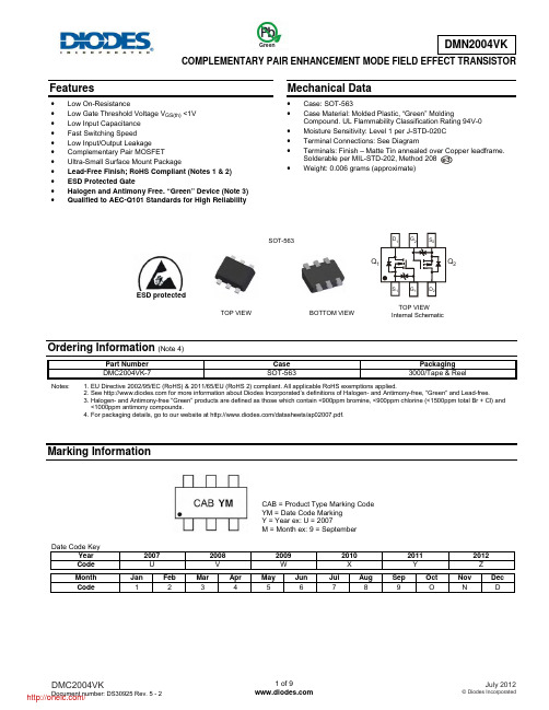
COMPLEMENTARY PAIR ENHANCEMENT MODE FIELD EFFECT TRANSISTORFeatures• Low On-Resistance • Low Gate Threshold Voltage V GS(th) <1V • Low Input Capacitance • Fast Switching Speed • Low Input/Output Leakage • Complementary Pair MOSFET • Ultra-Small Surface Mount Package • Lead-Free Finish; RoHS Compliant (Notes 1 & 2) • ESD Protected Gate • Halogen and Antimony Free. “Green” Device (Note 3) • Qualified to AEC-Q101 Standards for High ReliabilityMechanical Data• Case: SOT-563 • Case Material: Molded Plastic, “Green” MoldingCompound. UL Flammability Classification Rating 94V-0 • Moisture Sensitivity: Level 1 per J-STD-020C • Terminal Connections: See Diagram • Terminals: Finish – Matte Tin annealed over Copper leadframe.Solderable per MIL-STD-202, Method 208 • Weight: 0.006 grams (approximate)Ordering Information (Note 4)Part Number Case Packaging DMC2004VK-7SOT-563 3000/Tape & ReelNotes: 1. EU Directive 2002/95/EC (RoHS) & 2011/65/EU (RoHS 2) compliant. All applicable RoHS exemptions applied.2. See for more information about Diodes Incorporated’s definitions of Halogen- and Antimony-free, "Green" and Lead-free.3. Halogen- and Antimony-free "Green” products are defined as those which contain <900ppm bromine, <900ppm chlorine (<1500ppm total Br + Cl) and <1000ppm antimony compounds.4. For packaging details, go to our website at /datasheets/ap02007.pdf.Marking InformationDate Code KeyYear 2007 200820092010 20112012Code U V W X Y ZMonth Jan Feb Mar Apr May Jun Jul Aug Sep Oct Nov Dec Code 1 2 3 4 5 6 7 8 9 O N De3SOT-563TOP VIEWInternal SchematicTOP VIEW BOTTOM VIEWESD protectedQ 2CAB = Product Type Marking Code YM = Date Code Marking Y = Year ex: U = 2007 M = Month ex: 9 = September GreenMaximum Ratings N-CHANNEL – Q 1 (@T A = +25°C, unless otherwise specified.)Characteristic Symbol Value UnitDrain Source Voltage V DSS20 V Gate-Source Voltage V GSS±8 V Drain Current (Note 5) T A = +25°C T A = +85°CI D670480 mAMaximum Ratings P-CHANNEL – Q 2 (@T A = +25°C, unless otherwise specified.)Characteristic Symbol Value UnitDrain Source VoltageV DSS-20 V Gate-Source Voltage V GSS±8 V Drain Current (Note 5) T A = +25°C T A = +85°CI D-530-380 mAThermal CharacteristicsCharacteristic Symbol Value UnitPower Dissipation (Note 5) P D400 mW Thermal Resistance, Junction to Ambient (Note 5) R θJA 312.5 °C/W Operating and Storage Temperature RangeT j , T STG-65 to +150 °CNote:5. Device mounted on FR-4 PCB.Electrical Characteristics N-CHANNEL – Q 1 (@T A = +25°C, unless otherwise specified.)Characteristic SymbolMin Typ Max Unit Test Condition OFF CHARACTERISTICS (Note 6) Drain-Source Breakdown Voltage BV DSS 20 ⎯ ⎯V V GS = 0V, I D = 10µAZero Gate Voltage Drain Current I DSS ⎯ ⎯ 1.0 µAV DS = 16V, V GS = 0V Gate-Source LeakageI GSS ⎯ ⎯ ± 1.0µA V GS = ±4.5V, V DS = 0VON CHARACTERISTICS (Note 6) Gate Threshold VoltageV GS(th) 0.5 ⎯ 1.0 V V DS = V GS , I D = 250µAStatic Drain-Source On-Resistance R DS (ON)⎯ ⎯ ⎯ 0.4 0.5 0.7 0.550.70 0.90 Ω V GS = 4.5V, I D = 540mA V GS = 2.5V, I D = 500mA V GS = 1.8V, I D = 350mAForward Transfer Admittance |Y fs | 200 ⎯ ⎯ mS V DS =10V, I D = 0.2ADiode Forward Voltage (Note 6) V SD 0.5 ⎯ 1.2 V V GS = 0V, I S = 115mA DYNAMIC CHARACTERISTICS Input Capacitance C iss ⎯ ⎯ 150 pF V DS = 16V, V GS = 0Vf = 1.0MHz Output CapacitanceC oss ⎯ ⎯ 25 pF Reverse Transfer Capacitance C rss ⎯ ⎯ 20 pF Reverse Transfer CapacitanceC rss⎯⎯20 pFNotes: 6. Short duration pulse test used to minimize self-heating effect.Electrical Characteristics P-CHANNEL – Q 2 (@T A = +25°C, unless otherwise specified.)Characteristic SymbolMin Typ Max Unit Test Condition OFF CHARACTERISTICS (Note 6) Drain-Source Breakdown Voltage BV DSS -20 ⎯ ⎯V V GS = 0V, I D = -250µAZero Gate Voltage Drain Current I DSS ⎯ ⎯ -1.0 µAV DS = -20V, V GS = 0V Gate-Source LeakageI GSS ⎯ ⎯ ± 1.0µA V GS = ±4.5V, V DS = 0VON CHARACTERISTICS (Note 6) Gate Threshold VoltageV GS(th) -0.5 ⎯ -1.0 V V DS = V GS , I D = -250µAStatic Drain-Source On-Resistance R DS (ON)⎯ 0.7 1.1 1.7 0.91.42.0 Ω V GS = -4.5V, I D = -430mA V GS = -2.5V, I D = -300mA V GS = -1.8V, I D = -150mAForward Transfer Admittance |Y fs | 200 ⎯ ⎯ mS V DS =10V, I D = 0.2ADiode Forward Voltage (Note 6) V SD -0.5 ⎯ -1.2 V V GS = 0V, I S = -115mA DYNAMIC CHARACTERISTICS Input Capacitance C iss ⎯ ⎯ 175 pFV DS = -16V, V GS = 0Vf = 1.0MHzOutput CapacitanceC oss ⎯ ⎯ 30 pFReverse Transfer CapacitanceC rss⎯⎯20 pFNotes: 6. Short duration pulse test used to minimize self-heating effect.Q 1, N-CHANNELFig. 1 Typical Output CharacteristicsDS I , D R A I N C U R R E N T (A )Fig. 2 Typical Transfer CharacteristicsGS I , D R A I N C U R R E N T (A )D Fig. 3 Gate Threshold Voltage vs. Ambient TemperatureA V , G A T E T H R E S H O L D V O L T A G E (V )G S (t h)I , DRAIN CURRENT (A)Fig. 4 Static Drain-Source On-Resistancevs. Drain CurrentDI , DRAIN CURRENT (A)Fig. 5 Static Drain-Source On-Resistancevs. Drain CurrentD I , DRAIN-SOURCE CURRENT (A)Fig. 6 Static Drain-Source On-Resistance vs.Drain-Source Current vs. Gate Source VoltageDQ 1, N-CHANNEL (cont.)T , AMBIENT TEMPERATURE (°C)Fig. 7 Static Drain-Source On-State Resistancevs. Ambient TemperatureAFig. 9 Forward Transfer Admittance vs. Drain Current DV , DRAIN-SOURCE VOLTAGE (V)Fig. 10 Typical CapacitanceDSQ 2, P-CHANNEL-V , DRAIN SOURCE VOLTAGE (V)Fig. 11 Typical Output CharacteristicsDS -I , D R A I N C U R R E N T (A )DFig. 12 Typical Transfer CharacteristicsGS -I , D R A I N C U R R E N T (A )D Fig. 13 Gate Threshold Voltage vs. Ambient TemperatureA -V , G A T E T H R E S H O L D V O L T A G E (V )G S (t h)-I , DRAIN-SOURCE CURRENT (A)Fig. 14 Static Drain-Source On-Resistance vs. Drain CurrentD -I , DRAIN-SOURCE CURRENT (A)Fig. 15 Static Drain-Source On-Resistance vs.Drain CurrentDFig. 16 Static Drain-Source On-Resistance vs.Drain-Source Current vs. Gate Source VoltageDQ 2, P-CHANNEL (cont.)Fig. 17 Static Drain-Source On-State Resistancevs. Ambient TemperatureAFig. 19 Forward Transfer Admittance vs. Drain CurrentD -V , DRAIN-SOURCE VOLTAGE (V)Fig. 20 Typical CapacitanceDSPackage Outline DimensionsSuggested Pad LayoutSOT563Dim Min Max Typ A 0.15 0.30 0.20 B 1.10 1.25 1.20 C 1.55 1.70 1.60 D - - 0.50 G 0.90 1.10 1.00 H 1.50 1.70 1.60 K 0.55 0.60 0.60 L 0.100.30 0.20 M 0.10 0.18 0.11 All Dimensions in mmDimensions Value (in mm)Z 2.2 G 1.2 X 0.375 Y 0.5C11.7 C20.5 XZYC1C2C2GIMPORTANT NOTICEDIODES INCORPORATED MAKES NO WARRANTY OF ANY KIND, EXPRESS OR IMPLIED, WITH REGARDS TO THIS DOCUMENT, INCLUDING, BUT NOT LIMITED TO, THE IMPLIED WARRANTIES OF MERCHANTABILITY AND FITNESS FOR A PARTICULAR PURPOSE (AND THEIR EQUIVALENTS UNDER THE LAWS OF ANY JURISDICTION).Diodes Incorporated and its subsidiaries reserve the right to make modifications, enhancements, improvements, corrections or other changes without further notice to this document and any product described herein. Diodes Incorporated does not assume any liability arising out of the application or use of this document or any product described herein; neither does Diodes Incorporated convey any license under its patent or trademark rights, nor the rights of others. Any Customer or user of this document or products described herein in such applications shall assume all risks of such use and will agree to hold Diodes Incorporated and all the companies whose products are represented on Diodes Incorporated website, harmless against all damages.Diodes Incorporated does not warrant or accept any liability whatsoever in respect of any products purchased through unauthorized sales channel. Should Customers purchase or use Diodes Incorporated products for any unintended or unauthorized application, Customers shall indemnify and hold Diodes Incorporated and its representatives harmless against all claims, damages, expenses, and attorney fees arising out of, directly or indirectly, any claim of personal injury or death associated with such unintended or unauthorized application.Products described herein may be covered by one or more United States, international or foreign patents pending. Product names and markings noted herein may also be covered by one or more United States, international or foreign trademarks.LIFE SUPPORTDiodes Incorporated products are specifically not authorized for use as critical components in life support devices or systems without the express written approval of the Chief Executive Officer of Diodes Incorporated. As used herein:A. Life support devices or systems are devices or systems which:1. are intended to implant into the body, or2. support or sustain life and whose failure to perform when properly used in accordance with instructions for use provided in thelabeling can be reasonably expected to result in significant injury to the user.B. A critical component is any component in a life support device or system whose failure to perform can be reasonably expected to cause thefailure of the life support device or to affect its safety or effectiveness.Customers represent that they have all necessary expertise in the safety and regulatory ramifications of their life support devices or systems, and acknowledge and agree that they are solely responsible for all legal, regulatory and safety-related requirements concerning their products and any use of Diodes Incorporated products in such safety-critical, life support devices or systems, notwithstanding any devices- or systems-related information or support that may be provided by Diodes Incorporated. Further, Customers must fully indemnify Diodes Incorporated and its representatives against any damages arising out of the use of Diodes Incorporated products in such safety-critical, life support devices or systems.Copyright © 2012, Diodes Incorporated分销商库存信息: DIODESDMC2004VK-7。
- 1、下载文档前请自行甄别文档内容的完整性,平台不提供额外的编辑、内容补充、找答案等附加服务。
- 2、"仅部分预览"的文档,不可在线预览部分如存在完整性等问题,可反馈申请退款(可完整预览的文档不适用该条件!)。
- 3、如文档侵犯您的权益,请联系客服反馈,我们会尽快为您处理(人工客服工作时间:9:00-18:30)。
Number of Cycles at 60Hz
Fig.3- Typical Forward Characteristics
Fig.4- Typical Reverse Characteristics IR Instantaneous Reverse Current (mA)
IF Instantaneous Forward Current (A)
Note: 1. 8.3ms single half sine-wave superimposed on rated load (JEDEC method) 2. Pulse Test with PW = 300 µsec, 1% Duty Cycle. 3. P.C.B. mounted 5.0 x 5.0mm (0.2 x 0.2") copper pad areas.
TAITRON COMPONENTS INCORPORATED, SHANGHAI REPRESENTATIVE OFFICE
METROBANK PLAZA, 1160 WEST YAN’ AN ROAD, SUITE 1503, SHANGHAI, 200052, CHINA Tel: +86-21-5424-9942 Fax: +86-21-5424-9931
Rev. A/JJ 2007-06-15 Page 1 of 4
元器件交易网
1.0A Low Profile Chip Schottky Rectifier TSCDA12-TSCDA110
Typical Characteristics Curves
Fig.1- Forward Current Derating Curve IFSM Instantaneous Forward current (A) Ambient Temperature Ta (°C) Io(AV) Average Rectified Current (A) Fig.2-Max. Non-Repetitive Forward Surge Current
Maximum Ratings (T Ambient=25ºC unless noted otherwise)
Symbols Description Marking Code TSCDA12 S12 20 14 20 TSCDA14 S14 40 28 40 1.0 30 0.50 0.2 28.0 -55 to +125 -55 to +150 -55 to +150 0.70 0.85 TSCDA16 TSCDA110 S16 60 42 60 S110 100 70 100 V V V A A V mA ° C/W °C °C Unit
Rev. A/JJ 2007-06-15 Page 4 of 4
C2010 (SMA)
Mechanical Data
Case: Terminals: Polarity: Weight: Packed with FRP substrate and epoxy underfilled Pure Tin plated, solderable per MIL-STD-750, Method 2026 Laser cathode band marking 0.02 gram
TAITRON COMPONENTS INCORPORATED
Tel: (800)-TAITRON Fax: (800)-TAITFA (800)-824-8766 (800)-824-8329 (661)-257-6060 (661)-257-6415
元器件交易网
1.0A Low Profile Chip Schottky Rectifier TSCDA12-TSCDA110
1.0A Low Profile Chip Schottky Rectifier
Features
• • • • • Low Profile Package, Build-in Strain Relief Low Power Loss , High Efficiency High Surge Current Capability Super Very Low Forward Voltage Plastic Package has Underwriters Laboratory Flammability Classification 94V-0 • RoHS Compliant
TAITRON COMPONENTS INCORPORATED REPRESENTAÇÕES DO BRASIL LTDA
RUA DOMINGOS DE MORAIS, 2777, 2.ANDAR, SALA 24 SAÚDE - SÃO PAULO-SP 04035-001 BRAZIL Tel: +55-11-5574-7949 Fax: +55-11-5572-0052
TAITRON COMPONENTS MEXICO, S.A .DE C.V.
BOULEVARD CENTRAL 5000 INTERIOR 5 PARQUE INDUSTRIAL ATITALAQUIA, HIDALGO C.P. 42970 MEXICO Tel: +52-55-5560-1519 Fax: +52-55-5560-2190
C2010 (SMA)
How to contact us:
US HEADQUARTERS
28040 WEST HARRISON PARKWAY, VALENCIA, CA 91355-4162 Tel: (800) TAITRON (800) 824-8766 (661) 257-6060 Fax: (800) TAITFAX (800) 824-8329 (661) 257-6415 Email: taitron@
VRRM VRMS VDC Io(AV) IFSM VF IR RθJL TJ TSTG
Max. Recurrent Peak Reverse Voltage Max. RMS Voltage Max. DC Blocking Voltage Max. Average Forward Rectified Current (FIG.1) Peak Forward Surge Current (Note1) Max. Instantaneous Forward Voltage at 1.0A (Note2) Max. DC Reverse Current at Rated DC Blocking Voltage @Ta=25°C Typical Thermal Resistance, Junction to Lead (Note3) Operating Junction Temperature Range Storage Temperature Range
Rev. A/JJ 2007-06-15 Page 3 Chip Schottky Rectifier TSCDA12-TSCDA110
Dimensions in inch (mm)
VF Instantaneous Forward Voltage (V)
Percent of Rated Reverse Voltage (%)
Rev. A/JJ 2007-06-15 Page 2 of 4
元器件交易网
1.0A Low Profile Chip Schottky Rectifier TSCDA12-TSCDA110
Fig.5- Typical Junction Capacitance CJ Junction Capacitance (pF)
Reverse Voltage (V)
Marking Information: