UT165-L48_2 FLASH(Single)_STANDARD_V1.5
TL_81000_EN

Group standardTL 81000Issue 2021-09Class. No.:8MD00Descriptors:EMC, ESD, electrostatic discharge, immunity, interference emission, interference emission, interference immunity, pulseElectromagnetic Compatibility of Electronic Components for Motor Vehicles EMC changesPrevious issuesTL 965: 2012-04; TL 82066: 2006-11; TL 82166: 2011-01; TL 82366: 2008-02; TL 82466: 2009-06;TL 82566: 2011-05; TL 81000: 2013-02, 2014-04, 2016-02, 2018-03, 2021-06ChangesThe following changes have been made to TL 81000: 2021-06:a)Section 5.3.6.3 "Requirements": Formula for test no. "B9" adapted in column "QP";b)Section 5.4.2.5 "Test pulse 48a": Figure 33 added;c)Section 5.4.2.6 "Test pulse 48": Figure 34 added.ContentsPageScope .........................................................................................................................3Definitions ..................................................................................................................3Abbreviations .............................................................................................................6General ......................................................................................................................6General conditions and terms ....................................................................................6Temperature ...............................................................................................................6Run-in time .................................................................................................................6Test voltage ................................................................................................................7Test documentation ....................................................................................................7Function performance status classification (FPSC) ...................................................7Component level ........................................................................................................8Electrostatic discharge (ESD) ....................................................................................8General requirements for ESD component testing ....................................................9Tests at assembly level (packaging and handling) ...................................................11Tests at system level ................................................................................................13ESD documentation/test documents ........................................................................18Interference immunity ...............................................................................................18General requirements for the interference immunity tests of components ...............18BCI testing . (19)12344.14.1.14.1.24.1.34.1.44.1.555.15.1.15.1.25.1.35.1.45.25.2.15.2.2Always use the latest version of this standard.This electronically generated standard is authentic and valid without signature. A comma is used as the decimal sign.The English translation is believed to be accurate. In case of discrepancies, the German version controls.Page 1 of 110All rights reserved. No part of this document may be provided to third parties or reproduced without the prior consent of one of the Volkswagen Group’s Standards departments. | internal© Volkswagen AktiengesellschaftVWNORM-2019-10Page 2TL 81000: 2021-09Antenna ....................................................................................................................22Stripline ....................................................................................................................25Mobile radio communications test ............................................................................27Magnetic field test ....................................................................................................29Interference emission ...............................................................................................34Overview of emission tests and frequency ranges ...................................................34Specific interference emission terms, definitions, and abbreviations .......................35General requirements – HF emissions from component measurements .................35Limit classes .............................................................................................................37Artificial network (AN test) ........................................................................................37Antennas (RE test) ...................................................................................................38Stripline (SL test, optional) .......................................................................................43Clamp-on current probe (CP test, optional) .............................................................45Magnetic field coil 12 cm ..........................................................................................47Magnetic field coil 60 cm ..........................................................................................52Isotropic magnetic field coil 100 cm 2 ........................................................................55Pulse ........................................................................................................................60Test equipment .........................................................................................................60Pulse forms ..............................................................................................................62Pulsed interference on power supply cables ............................................................67Pulsed interference on sensor cables ......................................................................74Vehicle level .............................................................................................................81Interference emission ...............................................................................................81Frequency range during vehicle measurement ........................................................81Requirements ...........................................................................................................81Test setup .................................................................................................................81Antennas and related components ..........................................................................83Measurement receiver settings and limits for vehicle measurements ......................83Interference immunity ...............................................................................................88Interference immunity test (far field) .........................................................................88Mobile radio communications test with exterior antenna attached to the vehicle ....92Mobile radio communications test using portable mobile radio communicationsdevices in the vehicle interior ...................................................................................94Additional measurements in the free field ................................................................96Electrostatic discharge – ESD ..................................................................................96General requirements for the ESD vehicle tests ......................................................96Test setup and test conditions for tests at vehicle level ...........................................97Procedure for tests at vehicle level ..........................................................................97Applicable documents ..............................................................................................98Bibliography ...........................................................................................................100ESD ........................................................................................................................101Geometric setup of the ESD coupling structure for indirect discharges atsystem level ...........................................................................................................101Interference immunity .............................................................................................102Test severity levels for BCI testing .........................................................................102Conversion of dB(µA) into mA ................................................................................103Magnetic field – correlation between magnetic field strength H and magneticflux density B ..........................................................................................................103Emission .................................................................................................................105Measurements in the AM range .............................................................................105Subjective evaluation of interference suppression .................................................105Analog radio and TV ranges and radio applications . (105)5.2.35.2.45.2.55.2.65.35.3.15.3.25.3.35.3.45.3.55.3.65.3.75.3.85.3.95.3.105.3.115.45.4.15.4.25.4.35.4.466.16.1.16.1.26.1.36.1.46.1.56.26.2.16.2.26.2.36.2.46.36.3.16.3.26.3.378Appendix A A.1Appendix B B.1B.2B.3Appendix C C.1C.2C.2.1Page 3TL 81000: 2021-09Digital radio and TV ranges (DAB, DVB-T, etc.) .....................................................108Long-distance interference suppression ................................................................110C.2.2C.2.3ScopeThis standard covers and defines requirements and tests at the component level and vehicle level that are used to ensure the electromagnetic compatibility (EMC) of electronic assemblies and sys-tems with respect to:–Electrostatic discharges that can directly or indirectly couple into an assembly or into supplyand signal cables (during the installation process, during vehicle servicing, or during vehicle operation)–Radiated interference that can couple into a vehicle's supply and signal cables or into elec-tronic assemblies or systems–Pulse interference on power supply cables caused by electrical and electronic componentson power supply cables or on signal cables and sensor cables that are directly or indirectly (e.g., via switch contacts, relay contacts, or valves/actuators/sensors) galvanically connected to power supply cables–Pulse interference on sensor cables ; with the exception of cables that belong to the powersupply and therefore fall under "pulse interference on power supply cables"–Radio interference suppression and the associated limitation of the interference emission ofelectrical and electronic vehicle components –Magnetic fields that are generated DefinitionsTest method in which the charged test generator electrode is quickly brought close to the DUT; discharge takes place by means of a sparkover to the DUTCorresponds to the simple peak value or maximum value An assembly is an individual component or a combination of components,as delivered by the contractorGeneral term for an electronic component, assembly, or system (e.g., elec-tronic control unit [ECU], sensor, actuator).Test method in which the test generator electrode is brought intocontact with the DUT; discharge is then initiated by the discharge switch in-side the generatorCoupling is interference on cables caused by the transfer of power from one cable to another.A device with defined dimensions and characteristics used for the common mode coupling of a disturbance to the test circuit without a galvanic con-nectionA current transformer for coupling a disturbance into the test circuit with-out a galvanic connection to itOne or more functions of the device do not perform as designed during and after exposure to the disturbance and the device has to be repaired or re-placed or, if there is still functional capability, some parameters do not lie within the specified tolerances.12Air discharge (for ESD)Amplitude Assembly ComponentContact discharge (for ESD)CouplingCoupling clampCurrent injection probe DamagePage 4TL 81000: 2021-09When a device's operation is impaired in such a way that is not negligible but still accepted as permissible. Degradation ends when the disturbance subsides.Electronic component, assembly, or system under testA discharge that is discharged directly ontothe device under test (DUT).Electromagnetic quantity that can cause undesirable interference in electri-cal equipment. Disturbance serves as a generic term for such terms as in-terference voltage, interference current, interfering signal, and interferenceenergy.Time interval between the pulse's rise to over 10% of the amplitudeand its subsequent fall below this value.The ability of electrical equipment to function satisfactorily inan electromagnetic environment without unduly influencing its environment (including other equipment).Electromagnetic effects (e.g., fields) on circuits, assemblies,and systems (e.g., vehicle).The time required to fall from 90% to 10% of the amplitude Impairment of a device's function to a degree that is no longer permissibleand where the function can only be restored by technical intervention.This standard uses FPSC as per definition inISO 11452-1, ISO 7637-1, and ISO 10605. A detailed description can be found in section 4.1.5.Maximum height beyond the ripple amplitude.The discharge occurs onto a coupling structure in the vicinity of theDUT and simulates a discharge onto objects in the vicinity of the DUT, or discharges that flow in cables adjacent to DUT cables in the wiring harness.Disturbance emitted by an interference sourceThe ability of an electrical device to withstand specific disturbances withoutmalfunctionNon-periodic, brief positive or negative disturbance (voltage or current) be-tween two steady statesElectrical or electronic device whose function can be influenced by distur-bancesElectrical device of the vehicle from which disturbances are emitted, or ori-gin of disturbancesMinimum value of a disturbance that causes a malfunction in an interfer-ence sinkVoltage drop below the normal level, caused by the switch-ing on and turning of the starter. In engaging alternators, this interference usually includes an initial single pulse when the starter is switched on and a state while it is turning.A circuit that emits interference.Disturbance of the device's function to a degree that is no longer permissi-ble. The malfunction ends after the disturbance subsides.Undesirable impairment of a device's operation.The nominal voltage of the power supply system isspecified in order to be independent from the used battery technology.In this document, parallel routing describes cables following the same path within a wiring harness.DegradationDevice under test (DUT)Direct discharge (for electrostatic discharge (ESD))Disturbance Duration of single pulse (t d )Electromagnetic compatibility (EMC)Electromagnetic interference (EMI)Fall time (t f )Function failure Function performance status classification (FPSC)Height of single pulse (V, I)Indirect discharge (for ESD)Interference emission Interference immunity Interference pulse Interference sinkInterference source Interference threshold Interference when starting the engine Interfering circuitMalfunctionMalfunctionNominal voltage of the power supply system Parallel routingPage 5TL 81000: 2021-09Transitional process, during which the height of the ripple amplitude is ex-ceeded for a duration less than 150 µs. Peaks are generally oscillating and arise from high-frequency currents caused by sudden load changes. The duration of a decreasing oscillation is defined as less than 1/20 of the inter-val between two sequential peaks. Thus, decreasing oscillation after this time must regarded as ripple. Frequent causes of decreasing oscillations include ignition systems and rectifiers at the output of alternators.Energy per unit of time for subsiding peaks Time interval between the end of one pulse and the start of the followingpulse.Number of pulses per unit of time.A number of repeated pulses during a defined time interval.Interval between the instant in which the voltage increases above its normal value due to a transitional process and the point in time at which the volt-age drops back to its original value and remains there.The maximum change in voltage caused by ripple above or below the aver-age level is referred to as upper amplitude or lower amplitude. The ripple from amplitude to amplitude is defined by the maximum distance between the upper and lower amplitude.More or less periodic changes in voltage around the voltage level that oc-curs in the system in its steady state. Transitional processes and frequen-cies below 10 Hz are excluded (apart from the process of starting the en-gine).The time required to rise from 10% to 90% of the amplitude Cables that are not directly or indirectly (via switch contacts, relay con-tacts, or valves/actuators/sensors) galvanically connected to the power supply cablesA non-oscillating transitional process, usually occurring sporadically and in-frequently, which has a long duration in comparison to 150 µs and which exceeds the ripple amplitude.A condition that sets in after the activation operation and in which the val-ues of electrical variables remain essentially constant.The voltage measured at any arbitrarily chosen pair of terminals of the pow-er supply system, whereby one terminal may also be a ground connection.Within this context, "surfaces" refers not only to closed surfaces, but also to all gaps and openings (switches, tip switches, transition points, ventilation slots, loudspeaker openings, etc.).A system is defined as an assembly in conjunction with all components necessary for complete functioning (buttons, switches, antennas, displays,sensors, actuators, etc.).In the context of this standard, "test step" refers to the specified number of discharges that occur at a discharge point and that have a specific polarity and voltage.Temporary increase or decrease of the supply voltagecaused by rapid load changes.Terrestrial Trunked Radio (TETRA) frequency bands The vehicle electrical system in a motor vehicle that is used to pro-vide electrical power, including the connected battery and the alternator with regulator.PeakPeak power Pulse interval Pulse repetition frequency Pulse sequence Return timeRipple magnitudeRipplesRise time (t r )Signal or sensor cable Single pulseSteady state Supply voltageSurface (for ESD)SystemTest step (for ESD)Transitional process of supply voltage Trunked radioVehicle power supply systemPage 6TL 81000: 2021-09AbbreviationsAmplitude modulation Artificial networkAverage detector as per DIN EN 55016-1-1. Use of the linear average de-tector without consideration of the time constant of the display apparatus is also permissible.Bulk current injectionPublic safety organizations in GermanyIntermediate frequency (IF) measurement bandwidth of the test receiver Current probe Continuous waveDigital Audio BroadcastingDedicated short-range communication Device under testElectrostatic discharge Fast Fourier transformGlobal navigation satellite system (GPS, GLONASS, Beidou, Galileo, Qua-si-Zenith Satellite System [QZSS])Global Positioning SystemMetal-oxide-semiconductor field-effect-transistor Moving Picture Experts GroupPeak detector as per DIN EN 55016-1-1Pulse-width modulationQuasi-peak detector as per DIN EN 55016-1-1Quadrature phase-shift keying Radiated emissionSatellite Digital Audio Radio Service StriplineShort range devicesTerrestrial Trunked RadioUniversal Mobile Telecommunications SystemGeneralGeneral conditions and termsDeviations from the following test conditions must always be documented in the test record.TemperatureTest temperature range:(23 ±5) °C; in agreement with the purchaser, at operat-ing temperatureRun-in timeThe electrical components must be subjected to a 15 min run-in time under the specified load (as per drawing or Performance Specification) and with the test voltage.3 AM AN AVBCI BOS BW CP CW DAB DSRC DUT ESD FFT GNSS GPSMOSFET MPEG PK PWM QP QPSK RESDARS SL SRD TETRA UMTS 4 4.14.1.14.1.2Page 7TL 81000: 2021-09Test voltageOperating voltagesAs per drawing, Performance Specification, or table 1;unless otherwise specified, the following voltage values must be used:Table 1 – Operating voltages and test voltagesTest documentationThe following documents must be submitted when the development process starts:–System designation and description with a representation of the system functions –Circuit diagram, component location drawing, and bill of materials–Operating states with sequence descriptions (e.g., switch-on/off procedures, static/dynamic states)–Description of circuit parts (sub-systems, sensors, actuators)–System variants and codings–Interfaces to other vehicle components–Error handling and diagnostic functions of the system itself–Description of EMC measures (e.g., filter and protective circuitry of inputs/outputs as well as power supply cables, shielding measures)Before the samples to be tested are delivered, the following documents must be presented in addi-tion:–Exact schedule for the planned EMC component tests and the planned test location (laborato-ry)–Deviations from requirements of this standard that were made in agreement with the purchas-er and the contractor–Informative, complete EMC qualification report for the pertinent sample version –Hardware/software version with description of the EMC measuresFunction performance status classification (FPSC)For interference immunity tests and ESD, this standard uses the function performance status clas-sification (FPSC) as defined in ISO 11452-1, ISO 7637-1, and ISO 10605. The following status def-initions as specified in ISO 11452-1 are used:–Status I The function behaves as specified before, during, and after the test–Status IIThe function does not behave as specified during the test, but automatically returns to normal operation after the testThe following definitions from ISO 11452-1 are used to determine the status (I or II) that must be met and the disturbance (level) up to which this status must be met:4.1.3 4.1.4 4.1.5Page 8TL 81000: 2021-09–L1Disturbance level up to which status I must be met–L2Disturbance level up to which at least status II must be met (status I is per-missible as well)Deviating from the examples in ISO 11452-1, it is not the different functions of a DUT that are cate-gorized, but rather the effects or functional deviations of a DUT occurring during an interference immunity test. Based on how customers are affected, there are three categories of effects:–Category 1Minor effects or negligible malfunctions of the DUT–Category 2Effects or malfunctions of the DUT with an impact on comfort–Category 3All significant effects or other effects and malfunctions of the DUT that do not fall into category 1 or category 2The purchaser is solely responsible for categorizing the effects that occurred during testing. If a malfunction has not been assigned a category, it must always be assigned to category 3. Figure 1shows a diagram of the FPSC.Legend A Category 1B Category 2CCategory 31Status I 2Status IIyV/m, dB(μA), VFigure 1 – Diagram of the FPSCComponent levelThe contractor must perform all component tests as agreed in the test strategy.To obtain a release for the component from the purchaser, the component tests as per section 5and the full vehicle testing as per section 6 must be completed with positive results.Electrostatic discharge (ESD)ESD component tests are based on the following standards: DIN EN 61000-4-2 and ISO 10605.55.1Page 9TL 81000: 2021-09General requirements for ESD component testing Protection targetsThere must not be any permanent damage to an assembly caused by ESD during installation, ve-hicle servicing, or vehicle operation. In addition, discharges from persons in or at the vehicle must not cause malfunctions or function failures.Design measures must prevent components from becoming charged due to air flows or motion.The semiconductor subcomponents connected to the DUT terminals must pass this test without additional protective circuitry at the pertinent pins. If the semiconductor subcomponents in use do not meet these requirements, the assembly developer must justify how sufficient ESD interference immunity is achieved using other suitable protective measures.Test scope and test severitiesESD tests must be performed at the assembly, system, and vehicle levels.All test scopes in table 2 must be performed.5.1.1 5.1.1.15.1.1.2Page 10TL 81000: 2021-09Table 2 – Test scope overview5.1.1.3Test equipment and requirementsApart from the following exceptions, the test generator requirements as per DIN EN 61000-4-2 ap-ply:–It must be possible to select an energy storage capacitance between 150 pF and 330 pF.–The discharge resistance must be 330 Ω.–It must be possible to select an output voltage of up to ±15 kV for contact and air discharges.–The test generator's characteristics must be verified as per ISO 10605.–The relative humidity during the test must be between 20% and 60%.Before a test is performed, a test plan containing all items, operating states, and test severity levels to be tested must be prepared.A test starts with the lowest absolute test voltage and ends with the highest absolute test voltage.Either alternating polarities (e.g., +4 kV → -4 kV → … → +15 kV → -15 kV) or separate test runs with positive and negative test voltage (e.g., +4 kV → … → +15 kV → -4 kV → … → -15 kV) can be used.Unless otherwise agreed upon with the purchaser, the function must be checked and the event memory must be read out after each discharge voltage.Discharges cause charges to build up on conductive surfaces or connector pins. These charges must be dissipated before each new discharge.During discharge, the electrode must be kept as perpendicular to the DUT as possible. If this is not possible, an angle of at least 45° must be maintained.Tests at assembly level (packaging and handling)Test setup and test conditionsThe test setup for testing at assembly level is shown in figure 2. The requirements as persection 5.1.1.3 must be used. The test setup corresponds to the one described in ISO 10605. The DUT must be tested individually, i.e., as delivered by the contractor and without peripherals con-nected to it.The DUT must always be placed directly on the ground plate. An insulating base must not be used.In the case of metallic housings, the contact between the DUT and base must be established in such a way that good conductivity is ensured between them.The return conductor leading from the ESD generator to the ground connection must be fully rout-ed (no shortening) at the greatest possible distance to the ground plate.5.1.2 5.1.2.1Legend1Ground bus2Ground plate3DUT4Ground point5Wooden table6ESD generatorFigure 2 – Example of a test setup for testing at assembly levelProcedure5.1.2.2The contractor must perform the test at assembly level as per ISO 10605 with the specified addi-tions and changes.The test scope can be found in table 2.The tests must always be performed on three samples.For each discharge voltage and each polarity, at least 3 or 5 discharges must be performed for contact discharge, and at least 10 discharges for air discharge. Details can be found in table 2. The contact discharges onto pins must be performed in a defined manner on each individual pin (also for coaxial systems). If necessary, the pins must be extended using a piece of cable.In order to detect premature damage, the DUTs must be included in service life tests after the ESD tests are completed.Testing at the assembly level (packaging and handling) is considered passed if all of the following items are fulfilled:。
泰尔斯特极限移动宽带USB模块说明书

Removing the Modem 1. Exit the Connection Manager software. 2. Remove the modem by pulling it straight out from
the USB port.
Troubleshooting For a more complete listing of errors and possible solutions, please see the User Guide or Connection Manager online Help.
Starting the Mac Software If the Connection Manager software has not started automatically: Click the program’s icon in the dock. -orIn Finder™, select Go > Applications > Telstra Connection Manager and then double-click Telstra Connection Manager.
Problem/Error Solution
The device has no power— the LED in‑ dicator is off.
Ensure the following: • The device is properly inserted. • The computer is turned on and
Viewing the User Guide The User Guide provides additional operating informa‑ tion and specifications for the modem.
TI产品中文版说明书
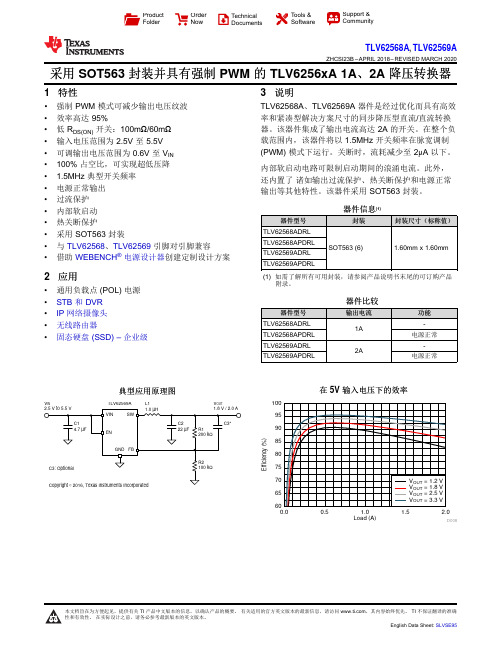
Load (A)E f f i c i e n c y (%)0.00.51.0 1.52.06065707580859095100D008V INV OUTL1TLV62569AProduct Folder Order Now Technical Documents Tools &SoftwareSupport &CommunityTLV62568A ,TLV62569AZHCSI23B –APRIL 2018–REVISED MARCH 2020采用SOT563封装并具有强制PWM 的TLV6256xA 1A 、2A 降压转换器1特性•强制PWM 模式可减少输出电压纹波•效率高达95%•低R DS(ON)开关:100m Ω/60m Ω•输入电压范围为2.5V 至5.5V •可调输出电压范围为0.6V 至V IN •100%占空比,可实现超低压降• 1.5MHz 典型开关频率•电源正常输出•过流保护•内部软启动•热关断保护•采用SOT563封装•与TLV62568、TLV62569引脚对引脚兼容•借助WEBENCH ®电源设计器创建定制设计方案2应用•通用负载点(POL)电源•STB 和DVR •IP 网络摄像头•无线路由器•固态硬盘(SSD)–企业级3说明TLV62568A 、TLV62569A 器件是经过优化而具有高效率和紧凑型解决方案尺寸的同步降压型直流/直流转换器。
该器件集成了输出电流高达2A 的开关。
在整个负载范围内,该器件将以1.5MHz 开关频率在脉宽调制(PWM)模式下运行。
关断时,流耗减少至2μA 以下。
内部软启动电路可限制启动期间的浪涌电流。
此外,还内置了诸如输出过流保护、热关断保护和电源正常输出等其他特性。
该器件采用SOT563封装。
器件信息(1)器件型号封装封装尺寸(标称值)TLV62568ADRL SOT563(6)1.60mm x 1.60mmTLV62568APDRL TLV62569ADRL TLV62569APDRL(1)如需了解所有可用封装,请参阅产品说明书末尾的可订购产品附录。
Micrel KSZ8851-16MLL 48-pin单端口以太网控制器与非PCI接口评估板用户指南

KSZ8851-16MLL48-pin Single-Port Ethernet ControllerWith 8-bit or 16-bit Non-PCI InterfaceEvaluation Board User’s GuideRevision 1.1August 2010© Micrel, Inc. 2007All rights reservedMicrel is a registered trademark of Micrel and its subsidiaries in theUnited States and certain other countries. All other trademarks are theproperty of their respective owners.The information furnished by Micrel in this datasheet is believed to be accurate and reliable. However, no responsibility is assumed by Micrel for its use. Micrel reserves the right to change circuitry and specifications at any time without notification to the customer. Micrel Products are not designed or authorized for use as components in life support appliances, devices or systems where malfunction of a product can reasonably be expected to result in personal injury. Life support devices or systems are devices or systems that (a) are intended for surgical implant into the body or (b) support or sustain life, and whose failure to perform can be reasonably expected to result in a significant injury to the user.Micrel, Inc. August 6, 2010A Purchaser's use or sale of Micrel Products for use in life support appliances, devices or systems is at Purchaser's own risk and Purchaser agrees to fully indemnify Micrel for any damages resulting from such use or sale.Revision HistoryRevisionDateSummary of Changes1.0 2/20/2008 Initial Release1.1 8/6/2010Add JP8 for connection between VDD_IO and 1.8V (if VDD_IO is 1.8V). Changed the LED pulled up to 3.3V.Table of Contents1.0Introduction (5)2.0Board Features (5)3.0Evaluation Kit Contents (5)4.0Hardware Description (6)4.1Host Interface (7)4.2Jumper Setting & Definition (8)4.3Power Supply and Test Point Definition (9)4.4RJ-45 Connector and Transformer (9)4.5EEPROM and LED Indicators (9)4.6Board Reset (10)5.0Bill of Materials (11)Micrel, Inc. August 6, 2010List of FiguresFigure 1. KSZ8851-16MLL Evaluation Board (6)Figure 2. KSZ8851-16MLL-Eval Host Interface Connection with Spirent SmartBits (7)List of TablesTable 1. Header JP1 – Host Interface Connection for SD[15:0] (7)Table 2. Header JP1 – Host Interface Connection for Control and Power (8)Table 3. KSZ8851-16MLL-Eval Jumper Definition (8)Table 4. KSZ8851-16MLL-Eval Test Point Definition (9)Table 5. KSZ8851-16MLL EEPROM Format (9)Table 6. KSZ8851-16MLL-Eval Port Status LED Definition (10)Table 7. KSZ8851-16MLL-Eval LED Definition (10)Micrel, Inc. August 6, 20101.0 IntroductionThe KSZ8851-16MLL-Eval Evaluation Board is intended to provide a convenient and fast way to evaluate or demonstrate the functionality and performance of this new Single-Port Ethernet Controller KSZ8851-16MLL device from Micrel.The KSZ8851-16MLL comes with a 48-pin, lead-free LQFP (7mm x 7mm) package and provides an ideal solution for applications requiring high-performance from single-port Ethernet Controller with 8-bit or 16-bit generic processor interface. The KSZ8851-16MLL offers the most cost-effective solution for adding high-throughput Ethernet connectivity to traditional embedded systems.This evaluation board is designed as a stand alone without microcontroller or M16C on board. By default the KSZ8851-16MLL-Eval board comes with an operation of 16-bit bus mode, Little Endian mode and disabled EEPROM for KSZ8851-16MLL device. Customer may wire the board for his desired interface. The purpose is to provide a simple tool that can be used to evaluate the KSZ8851-16MLL device by connecting via headers to customer provided Microcontroller or Non-PCI hardware platform.Micrel provides a basic software driver based on the 8 or 16-bit bus solution and different operating system platforms to evaluate the KSZ8851-16MLL functionality and performance. The software includes a configuration utility to allow quick and easy device setup, initialization and transmit/receive packet. All KSZ8851-16MLL configuration pins and host interface signals are accessible either by jumpers, test points or headers.2.0 Board Features•One KSZ8851-16MLL 48-pin Single-Port Ethernet Controller with shared data bus for host interface•Single +5V/GND power input from headers•RJ-45 Jack for Fast Ethernet cable interface•HP Auto-MDIX for automatic detection and correction for straight-through and crossover cables•Two on board LDO voltage regulators, one for VDD_IO and the other for VDD_A3.3•One AT93C46 for external EEPROM interface•Two LED indicators for port status and activity•One LED indicator for 3.3V output ready•One LED indicator for Power Management Event (PME) output status•Jumpers to configure strapping pins and VDD_IO voltage option•Headers to wire the host interface from external hardware platform•Manual reset button for quick reboot after re-configuration of strapping pins3.0 Evaluation Kit ContentsThe KSZ8851-16MLL Evaluation Kit includes the following hardware:•KSZ8851-16MLL Evaluation BoardThe KSZ8851-16MLL Data Sheet and Hardware Design Package with the following collaterals that can be downloaded from Micrel’s website at •KSZ8851-16MLL Eval Board Schematic (PDF and OrCAD DSN file)•KSZ8851-16MLL Eval Board Gerber File (PDF version included)•KSZ8851-16MLL Eval Board User’s Guide (this document and included BOM)•KSZ8851-16MLL IBIS ModelMicrel, Inc. August 6, 20104.0 Hardware DescriptionThe KSZ8851-16MLL-Eval (shown in Figure 1) comes in a compact form factor and plugs directly into industry standard test equipment such as Spirent SmartBits, the other side of board is wired to external host interface through headers. Configuration of the KSZ8851-16MLL is accomplished through on-board jumper selections and/or by register access via the host shared data/control bus Interface.Figure 1. KSZ8851-16MLL Evaluation Board (Rev 1.1)Other features include a RJ-45 Jack for Fast Ethernet cable connection, transformer (Pulse H1102) to block DC level and provide a true AC coupling, EEPROM (Atmel AT93C46) to load MAC address when it is enabled, jumper to select LDO output for VDD_IO voltage, programmable LED indicators for reporting port link status and activity, and a manual reset button for quick reboot after re-configuration of strapping pins.The KSZ8851-16MLL-Eval receives +5V DC input power supply from its Headers JP1.Micrel, Inc. August 6, 2010Micrel, Inc. August 6, 20104.1 Host InterfaceThe KSZ8851-16MLL-Eval board receives +5V power from the header JP1 (pin 1/3). Figure 2 shows the Host interface connection with Spirent SmartBits for system set-up and performance test.Figure 2. KSZ8851-16MLL-Eval Host Interface Connection with Spirent SmartBitsThe KSZ8851-16MLL-Eval has a 40-pin header (JP1) for Host interface to external any Non-PCI hardware platform. Table 1 lists Shared Data SD[15:0] pin outs for the Host interface on header JP1. Table 2 lists the rest of control signals and power/ground pin outs for the Host interface on header JP1.16-Bit Bus Mode (pin 1 pull-up) 8-Bit Bus Mode (pin 1 pull down) Pin # (JP1) Shared Data Bus Signal CMD = 0 (low) CMD = 1 (high) CMD = 0 (low) CMD = 1 (high) 20 SD0 D0 x (don’t care) D0 A0 19SD1D1 x (don’t care) D1 A1 18 SD2 D2 A2 D2 A2 17 SD3 D3 A3 D3 A3 16 SD4 D4 A4 D4 A4 15 SD5 D5 A5 D5 A5 14 SD6 D6 A6 D6 A6 13 SD7 D7 A7 D7 A7 12 SD8 D8 x (don’t care) GND GND 11 SD9 D9 x (don’t care) GND GND 10 SD10 D10 x (don’t care) GND GND 9SD11D11 x (don’t care) GND GND 8 SD12 D12 BE0 GND GND 7 SD13 D13 BE1 GND GND 6 SD14 D14 BE2 GND GND 5 SD15D15BE3GNDGNDTable 1. Header JP1 – Host Interface Connection for SD[15:0]Pin # (JP1) Power & ControlSignal NamesDescription1, 3 5.0V_IN +5V power supply inputs for this board 2, 4, 21, 22, 25,26, 29, 33, 34, 37, 38, 39, 40 GND Groundinputs/pins23 CPU_CSN Chip Select input from host CPU24 CPU_RSTN Reset input from host CPU27 CPU_PME Power Management Event output to host CPU28 CPU_CMD Command type input from host CPU31 CPU_INTRN Interrupt output to host CPU35 CPU_WRN Write input from host CPU36 CPU_RDN Read input from host CPU30, 32 Spares For customer to useTable 2. Header JP1 – Host Interface Connection for Control and Power4.2 Jumper Setting & DefinitionThe KSZ8851-16MLL-Eval does not require any jumper for normal operation except the VDD_IO option. During power-up, the KSZ8851-16MLL is configured using the chip’s internal pull-up and pull-down resistors with its default strapping pin values which will set this device in operation of 16-bit bus mode, little endian and without EEPROM. Jumpers are provided to override the default settings, allowing for quick configuration and re-configuration of the board. To override the default settings, simply select and close the desired jumper setting(s) and toggle the on-board manual reset button (S1) for the new setting(s) to take effect.The KSZ8851-16MLL-Eval jumper settings are defined in Table 3 below.Jumper Definition Setting DescriptionJP2 EED_IO OFF (Default) OFF: EEPROM is not presentON: EEPROM is presentJP3 3.3V ON (Default) ON: to select 3.3V for VDD_IO (JP5 and JP6 must be OFF)OFF: De-select 3.3VJP4 EESK OFF (Default) OFF: Little EndianON: Big EndianJP5 2.5V OFF (Default) ON: to select 2.5V for VDD_IO (JP3 and JP6 must be OFF)OFF: De-select 2.5VJP6 1.8V OFF (Default) ON: to select 1.8V for VDD_IO (JP3 and JP5 must be OFF)OFF: De-select 1.8VJP7 P1LED1 OFF (Default) OFF: 16-Bit bus modeON: 8-Bit bus modeJP8 VDD_IO OFF (Default) OFF: VDD_IO = 2.5V or 3.3VON: VDD_IO = 1.8VTable 3. KSZ8851-16MLL-Eval Jumper DefinitionMicrel, Inc. August 6, 2010Power Supply and Test Point DefinitionThe KSZ8851-16MLL-Eval is supplied from external +5.0V DC power through a jumper (pin 1 and 3 at JP1), this +5.0V DC input is converted to both +3.3V with a Micrel LDO voltage regulator (U3, MIC5209BM) for VDD_A3.3 analog power and VDD (option for 3.3V, 2.5V or 1.8V) with a Micrel LDO voltage regulator (U5, MIC5209BM) for VDD_IO digital power. The KSZ8851-16MLL contains an internal +1.8V LDO, to provide its core, analog and PLL voltages.The KSZ8851-16MLL-Eval has four test points. They are defined in the following Table 4.Test Point DefinitionTP1 Power supply measurement for VDD_IOTP2 Power supply measurement for VDD_A3.3TP3 1.8V digital core voltage output measurement fromKSZ8851-16MLL internal LDOTP4 External power supply 5.0V_IN measurementTable 4. KSZ8851-16MLL-Eval Test Point Definition4.3 RJ-45 Connector and TransformerThe RJ-45 Jack (J1) connects to standard CAT-5 Ethernet cable to interface with 10Base-T/100Base-TX Ethernet devices. The LAN interface on the KSZ8851-16MLL is connected to a transformer (T1) with 50 ohm termination resistors for both TX+/- and RX+/- differential pairs. The line side of the transformer is connected to the RJ-45 connectors (J1).J1 also supports Auto-MDIX and Auto-Negotiation / Forced Modes.4.4 EEPROM and LED IndicatorsIt is optional in the KSZ8851-16MLL to use an external EEPROM. The EED_IO (JP2) must be pulled high (ON) to use external EEPROM.An external serial EEPROM with a standard microwire bus interface is used for non-volatile storage of information such as the host MAC address. The KSZ8851-16MLL can detect if the EEPROM is either a 1KB (93C46) or 4KB (93C66) EEPROM device. The EEPROM must be organized as 16-bit mode.The KSZ8851-16MLL EEPROM format is given in Table 5.WORD 15 8 7 00H Reserved1H Host MAC Address Byte 2 Host MAC Address Byte 12H Host MAC Address Byte 4 Host MAC Address Byte 33H Host MAC Address Byte 6 Host MAC Address Byte 54H – 6H Reserved7H-3FH Not used for KSZ8851-16MLL (available for user to use)Table 5. KSZ8851-16MLL EEPROM FormatMicrel, Inc. August 6, 2010A dual LED indicator (LED1) is located adjacent to the RJ-45 Connector (J1). The top LED is connected to P1LED1 (pin 1) and bottom LED is connected to P1LED0 (pin 2) of the KSZ8851-16MLL.The two LEDs are programmable to LED mode ‘0’ or ‘1’ via register 0xC6 bits [9], and are defined in the following Table 6.LED Mode0 (Default) 1LED1 (Top) 100BT ACTLED1 (Bottom) LINK/ACT LINKTable 6. KSZ8851-16MLL-Eval Port Status LED DefinitionTable 7 shows the rest of LEDs definition.LED Color DescriptionLED2 Green Power Management Event (PME) StatusLED3 Red 3.3V Power available indicatorTable 7. KSZ8851-16MLL-Eval LED Definition4.5 Board ResetThe KSZ8851-16MLL-Eval generates a reset signal from the reset circuitry during power up. It also provides a push button S1 reset circuit to reset the KSZ8851-16MLL device. During power up, the board is automatically reset. User can also press reset button S1 on the board for a manual reset.Micrel, Inc. August 6, 2010KSZ8851-16MLL-Eval Evaluation Board User’s Guide Rev. 1.1 Micrel, Inc.August 6, 201011/11 5.0 Bill of MaterialsKSZ8851-16MLL Eval Board (Revision 1.1)。
联盛UT165量产使用手册中文版

Hidden Block Partition: Auto: 量 File System: FAT32 來 Volume Label:
USB 2.0
8
无忧存储论坛
无忧存储网
UT165 MP Tool User’s Manual
flash bad block 連 行 F12 兩 滑 便 行 Format 來 料 參 不 bad block information
”F7” F7 Flash
无忧存储网
量
Version 4.0 AUGUST 13, 2008
All rights strictly reserved. Any portion of this paper shall not be reproduced, copied, or translated to any other forms without permission from Afa Technologies Inc.
歩:
Disk
歩:
1
(
來
)
Save
六歩:
行 MP
Disk
1
(
類
)
7
无忧存储论坛
无忧存储网
UT165 MP Tool User’s Manual 5.
說 :
量 Partition Firmware 量
[Capacity] 不 來 來 [Firmware ID]
USB VID/PID
來
[USB VID/PID]
來
[Inquiry Strings]
[Serial Number] [Write Protect] Yes No 來 Flash Size 粒數 [Flash ID]
NUC微控制器产品系列说明书

M251 Feature
。 Arm® Cortex®-M23 。 运行速度可达 48 MHz
M252 Feature
。 USB 2.0 全速设备无需外 挂晶振
M253 Feature
。 USB 2.0 全速设备无需外 挂晶振
。 高达五路 UART 。 CAN FD x1
2
Low Power
TrustZone
AEC-Q100
Market Trend
随着电子应用对低功耗或电池供电的需 求日益增加,现今的应用必须尽量降低 能源消耗,甚至在极端情况下,可能需 要倚赖单颗电池来维持长达 15 至 20 年 运转
低功耗应用情景包含手持式设备、居家、 AIoT、IIoT (工业物联网) 等应用情景, 使用范围十分广泛
(Programmable Serial I/O) • USB 2.0 全速装置无需外挂晶振 • 独立的 RTC 电源 VBAT 管脚
Highlight
• 支持 1.8 V ~ 5.5 V 串行接口,可连接不同电压 装置
*USCI: Universal Serial Control Interface Controller
C
1.8 3.3 5 M253
CU
3.3 5 M071
1.8 3.3 5 M252
U
3.3 5 M051
1.8 3.3 5 M251
3.3 5 Mini51
3.3 5 3.3 5
1.8 3.3 Nano100
M480 M460 M471 M453 M452 M451
E CU E CU
U C
U
Arm9™
瑞士比特U-400系列产业级USB闪存模块数据手册说明书

U-400 Series (USB2.0, high speed, SLC) Industrial USB Flash Drive Module (e USB) – 1 to 16GByte Main Features∙USB2.0 solid state flash drive for internal 9(10)-pin USB connector terminalo Fully compliant with USB specification 2.0/3.0 (High-Speed, 480Mb/s burst)o Fully backward compliant with USB 1.1 systems (Full speed, 12Mb/s burst)o Dimension of 26.65 x 36.8mmo 2.54mm or 2.00mm connector with keyed pin9(optional different key pins and pinouts)o Screw hole not connected (optional grounded)o Fix drive (optional removable)o LED for operation indicationo Write protect switch (optional)o FAT32 preformattedo Diagnostic features with Life Time Monitoring tool supporto Firmware update in field possible∙High performance 2.0 specificationo Up to 40 IOPS write and 1700 IOPS read (4KByte transfers)o Up to 34MBytes/s sequential write and 36MBytes/s read speed∙Power Supply: (Low-power CMOS technology)o 3.1 to 5.5V operating voltage∙Optimized FW algorithms especially for high read access and long data retention applications o Patented power-off reliability technologyo Near Miss ECC technologyMinimize the risk of uncorrectable bit failure over the product life time. Each read commandanalyzes the ECC margin level and refresh data if necessary.o Read Disturb ManagementThe read commands are monitored and the content is refreshed when critical levels have occurred.o Wear Leveling technologyEqual wear leveling of static and dynamic data. The wear leveling assures that dynamic data as wellas static data is balanced evenly across the memory. With that the maximum write endurance of thedevice is guaranteed.o Data Care ManagementThe interruptible background process maintain the user data for Read Disturb effects or Retentiondegradation due to high temperature effects.o UBER <10-17∙High reliabilityo SLC NAND Flash with highest program erase cycles per blocko Designed with sophisticated firmware architecture for industrial and netcom market especially 24/7 application like networking, base stations, infrastrucuture systems, POS/POI, medical and generalboot medium use case.o The product is optimized for highest reliability and power fail safety.o Commercial and Industrial Temperature range, 0° up to 70°C and -40° up to 85°C ∙Controlled BOM & PCN process∙RoHS, China-RoHS, REACH compatible, WEEE, CE, FCC compliant∙Customized options like registers, removable device, connector options, write protect switch, grounded mounting hole, conformal coating, densities, uploads, label, security controller, …1Table of ContentMAIN FEATURES (2)1 TABLE OF CONTENT (3)2 ORDER INFORMATION (4)2.1S TANDARD PRODUCTS WITH 2.54MM (J) CONNECTOR (4)2.2L OW PROFILE PRODUCTS WITH 2.00MM (K) CONNECTOR (4)2.3O FFERED OPTIONS FOR CUSTOM PRODUCTS (4)3 NAND FLASH TECHNOLOGIES (4)4 CAPACITY SPECIFICATION (5)5 SYSTEM PERFORMANCE (5)6 INTERFACE / PIN OUT (5)7 ELECTRICAL SPECIFICATION (6)8 ENVIRONMENTAL SPECIFICATION AND RELIABILITY (7)8.1R ECOMMENDED OPERATING CONDITIONS (7)8.2R ELIABILITY (7)8.3E NVIRONMENTAL -S HOCK,V IBRATION, AND H UMIDITY (7)9 COMPATIBILITY & COMPLIANCE (7)10 APPLICATIONS (8)11 STANDARD FORM FACTORS AND HARDWARE (8)12 BEST PRACTICES (11)12.1D EVICE R EMOVAL &P OWER F AILURE (11)12.2L IFETIME END HANDLING (11)13 PART NUMBER DECODER (12)14 LABEL (13)15 REVISION HISTORY (14)2Order Information2.1 Standard products with 2.54mm (J) connector2.2 Low profile products with 2.00mm (K) connectort = temperature grade (C=0°C to 70°C and I=-40°C to +85°C)2.3 Offered options for custom products∙Removable or fixed drive (standard fix)∙Customer specified strings and IDs∙FAT16, FAT32 format or customer file system, default FAT32∙Preload service∙Temperature rangePlease ask our sales for more details and additional features.3NAND Flash technologiesSLC, pSLC and MLC flasho Single-level-cell (SLC) flash, 1 bit (1 level) is stored in each memory cello Pseudo Single-level-cell (pSLC) 1 bit (1 level) is stored in an MLC memory cell by special sequenceso Multi-level-cell (MLC) flash, 2 bit (3 level) are stored in each memory cellDifferences5 System performance2) performance measured with Crystal Disk Mark performance test6 Interface / Pin out∙ USB-connector 10pin (2mm or 2.54mm pitch)∙ USB 2.0 high speed interface, USB1.1 full speed compatible ∙STD variation2 4 6 8 101 3 5 78Environmental Specification and Reliability8.1 Recommended operating conditionsi.e. retention acceleration factor is 700)8.2 Reliability8.3 Environmental - Shock, Vibration, and Humidity9Compatibility & Compliance∙Configurable as boot-drive∙Standard fix Configuration (mounted as local drive, not as removable drive)∙Operating Systems:o Windows CEo Windows Server 2003 and 2008o Windows 10, 8, 7, Vista, XP, 2000, MEo Mac 9.0 and newero Mac 8.6 (with driver) and newero Linux 2.4 and newero All USB mass-storage host systems (guarantee on all USB-IF certified systems) ∙CE – EN 55022/55024∙FCC class B for information technology∙USB-IF high speed certified∙RoHS∙UL60950 compliant PCB∙WEEE10 Applications∙ Gaming∙ Industrial PCs∙ Point-Of-Sale (POS) ∙ Industrial Automation ∙ Networking Equipment ∙ Medical Equipment ∙Data Recorders11 Standard form factors and hardware∙ Standard form factor of PCBs 36.8mm x 26.65mm ∙ Hole for mechanical fixture (optional grounded) ∙ Shield (connector Pin 10) grounded (optional NC) ∙ 2 additional holes∙ LED for operation indication (optional no LED) ∙ 2 connector typeso 2.54mm pitch, 7.5mm long standard o 2.00mm pitch, 3.6mm long low profile ∙Component heights max. 1.6mm on connector side max. 1.2mm on flash sideFigure 1: Mechanical Dimensions for 2.54mm connector (standard)Figure 2: Mechanical Dimensions for 2.00mm connector (low profile)Variationst = temperature grade (C=0°C to 70°C and I=-40°C to +85°C) f = firmware generation per product typeConnector tolerance0.25mmFigure 3: Component region on connector side (general tolerance ±0.5mm)Figure 4: Component region on flash side (symmetric to center line, general tolerance ±0.5mm)12Best PracticesThere are a number of best practices to reach the maximum life time.12.1 Device Removal & Power FailureUser data can be lost or corrupted if power is interrupted while the UFD is writing data. To avoid data loss, it is necessary to avoid power interruption while the device is busy. This can be made sure by always using the host (e.g. Windows) shutdown mechanisms or by detaching the device in the operating system before unplugging it. Swissbit also offers an Application Note “Design-In Guide” that describes techniques to reduce data loss on power failure, if power failure absolutely can’t be avoided.12.2 Lifetime end handlingIf the flash reaches its end of life, the number of bad blocks will increase (bad flash blocks will be replaced with spare blocks). There exist different side effects with negative data influence by degraded flash cells. Sometimes bit errors can occur because of effects that are not immediately detected by the flash, e.g. effects like program disturb or read disturb, which means that the bad block recognition does not always prevent data loss.When the number of bit errors in a sector exceeds the ECC correcting capabilities, invalid (uncorrected) data cannot be read from the host. Because of these effects it is strongly recommended to replace devices that are nearing their end of life. One good indicator would be the current spare blocks should not be reducing below 5. It is in the responsibility of the system integrator to account for the flash usage. Swissbit offers support for calculating expected life time if the exact use case is provided (e.g. by providing low level [USB interface] write statistics).For notes on reducing flash stress, Swissbit offers an Application Note called “Design-In Guide”.Please contact your sales channel for more information or send a mail to ******************.13Part Number DecoderS F UI 016G J 1 A B 1 TO - I - Q T - 211 - STDTemp. OptionFlash vendor Code1.Manufacturer2.Memory Type3.Product Type4.Density5.Platform6.Product Generation7.Memory Organization8.Technology9.Number of Flash chips10.Flash Code11.Temp. Option12.DIE Classification13.PIN Mode14. UFD XYZ15. Option14 LabelSFUIxxxxxxABxxx Part Number -x-xx-xxx-xxx 60xxxxxx Lot Code 6xxxxx Type No.SFUIxxxxxxABxTO -x-xx-xxx-xxx 60xxxxxx 6xxxxx15Revision HistoryDisclaimer:No part of this document may be copied or reproduced in any form or by any means, or transferred to any third party, without the prior written consent of an authorized representative of Swissbit AG (“SWISSBIT”). The information in this document is subject to change without notice. SWISSBIT assumes no responsibility for any errors or omissions that may appear in this document, and disclaims responsibility for any consequences resulting from the use of the information set forth herein. SWISSBIT makes no commitments to update or to keep current information contained in this document. The products listed in this document are not suitable for use in applications such as, but not limited to, aircraft control systems, aerospace equipment, submarine cables, nuclear reactor control systems and life support systems. Moreover, SWISSBIT does not recommend or approve the use of any of its products in life support devices or systems or in any application where failure could result in injury or death. If a customer wishes to use SWISSBIT products in applications not intended by SWISSBIT, said customer must contact an authorized SWISSBIT representative to determine SWISSBIT willingness to support a given application. The information set forth in this document does not convey any license under the copyrights, patent rights, trademarks or other intellectual property rights claimed and owned by SWISSBIT. The information set forth in this document is considered to be “Proprietary” and “Confidential” property owned by SWISSBIT.ALL PRODUCTS SOLD BY SWISSBIT ARE COVERED BY THE PROVISIONS APPEARING IN SWISSBIT,S TERMS AND CONDITIONS OF SALE ONLY, INCLUDING THE LIMITATIONS OF LIABILITY, WARRANTY AND INFRINGEMENT PROVISIONS. SWISSBIT MAKES NO WARRANTIES OF ANY KIND, EXPRESS, STATUTORY, IMPLIED OR OTHERWISE, REGARDING INFORMATION SET FORTH HEREIN OR REGARDING THE FREEDOM OF THE DESCRIBED PRODUCTS FROM INTELLECTUAL PROPERTY INFRINGEMENT, AND EXPRESSLY DISCLAIMS ANY SUCH WARRANTIES INCLUDING WITHOUT LIMITATION ANY EXPRESS, STATUTORY OR IMPLIED WARRANTIES OF MERCHANTABILITY OR FITNESS FOR A PARTICULAR PURPOSE.©2017 SWISSBIT AG All rights reserved.。
TiWi-uB2 EM BOARD User Guide
T I W I-U B2EM B OARDUser GuideLast updatedMay 28th, 2013Table of Contents1Introduction (3)1.1Purpose & Scope (3)1.2Applicable Documents (3)1.3Revision History (3)2TiWi-uB2 Module Description (4)3TiWi-uB2 EM Board Hardware (5)3.1Antenna (5)3.2Connectors (5)3.3Required Signals between EM Board and Host Device (6)3.4Connecting EM Board to Host Platform (7)3.5Power Supply (7)3.6Serial Interfaces (7)3.7HCI UART (8)3.8PCM Interface (8)3.9Option 1: Using EM Connectors (8)3.10Option 2: Using Single Row Headers (11)3.11Using J7 with USB to Serial Converter (12)4Schematic (13)4.1Bill Of Material (BOM) (14)5Application Development (15)5.1Overview (15)5.2Development Tools (15)6Contacting LS Research (20)1Introduction1.1 Purpose & ScopeThe purpose of this document is to provide details regarding the setup and use of theTiWi-uB2 module on an EM board. This document covers a description of the EM board and its features and a brief tutorial on how to operate the module EM board.1.2 Applicable Documents∙TiWi-uB2 Datasheet (330-0100)∙TiWi-uB2 Antenna Design Guide (330-0106)1.3 Revision HistoryTable 1 Revision History2TiWi-uB2 Module DescriptionThe TiWi-uB2 EM “Evaluation Module” Board is an evaluation platform for the LSResearch TiWi-uB2 Bluetooth and Bluetooth Low Energy (BLE) module.Communication between the TiWi-uB2 module, which is a slave, and the host device is through a UART interface.The TiWi-uB2 EM Board contains an on board chip antenna and U.FL connector. The EM board is intended for evaluation purposes when used in conjunction with variousTexas Instruments MSP430 and Stellaris development boards.Figure 1 TiWi-uB2 EM Board TopFigure 2 TiWi-uB2 EM Board Bottom3 TiWi-uB2 EM Board Hardware 3.1 AntennaThe TiWi-uB2 EM Board contains an on board chip antenna which is modular certified for FCC 15.247 and IC RSS-210, as well as compliant to the RF requirements for ETSI EN 300 328 and ETSI EN 301 489. The antenna layout and circuitry on the EM Board can be replicated on a custom designed PCB assembly. Assuming the design/layout is followed exactly as that which is on the EM Board, the custom PCB will retain the modular certification. Below are details on the certifications.FCC ID: TFB-BT1, 15.247 IC ID: 5969A-BT1, RSS 2103.2 ConnectorsThere are two primary connectors on the TiWi-uB2 EM Board (J1 & J2). These provide a standard interface to Texas Instruments development platforms (See Section 3.9). Two additional non populated connectors (J4 & J5) provide access to all of the significant signals on the module on a standard, single row 2mm pitch header.165423789Figure 3 TiWi-uB2 EM Board Top Side ConnectorsTable 2 TiWi-uB2 EM Board Top Side Connectors3.3 Required Signals between EM Board and Host DeviceIn addition to power and ground, there are three signals required for connecting a TiWi-uB2 module to a host device. See Table 3 below for details on these connections.Table 3 TiWi-uB2 Required Connections3.4 Connecting EM Board to Host PlatformThe TiWi-uB2 EM Board is intended to allow for evaluation of and early developmentwith a TiWi-uB2 module. The EM Board has two “EM” connectors on the bottom of the board that allows for easy connection to various Texas Instruments microcontrollerdevelopment platforms. The primary development platform is the MSP430F5438Experimenter Board.It is also possible to adapt the TiWi-uB2 EM Board to work with microcontroller platforms that do not have support for the EM connectors. Sections 3.9 and 3.10 describe the two options for adapting an EM Board to work with other microcontroller platforms.3.5 Power Supply3.5.1 VBATVBAT requires a 3.0V to 4.8V DC power supply.3.5.2 VDD_IOVDD_IO requires a 1.8V DC power supply.Figure 4 Power Supply3.6 Serial InterfacesThere are two serial interfaces to the module, HCI UART and PCM. Each interface isdescribed below.Figure 5 Serial Interfaces3.7 HCI UARTThis is the main interface between the host microcontroller and the module. TheBluetooth UART may also be used to download external patches from the host to theTiWi-uB2. The UART interface supports baud rates from 9600bps to 4Mbps.BT debug pin: The debug interface (TX_DBG) helps customers to debug the HW/SWissues for their application (not pictured).3.8 PCM InterfaceThe PCM Interface can connect to linear PCM Codec devices in master or slave mode.In master mode, the TiWi-uB2 generates the PCM_CLK and PCM_SYNC signals, and in slave mode, these signals are provided by another master on the PCM interface and are inputs to the TiWi-uB2.Figure 6 PCM Interface3.9 Option 1: Using EM ConnectorsEither build a PCB which has the EM Board mating connectors which will allow forplugging the TiWi-uB2 EM Board into, or solder wires to EM Board mating connectorsthat can then be wired into whatever development platform is being used.Below are two suggestions for the mating EM connectors.Through hole connector: Samtec TFM-110-01-S-D-WTSurface Mount connector: Samtec SFM-110-02-L-D-AIf building a PCB that has the mating EM Board connectors, the connectors need to be lined up and spaced 1.2” apart as shown in Figure 7.Figure 7 Host PCB EM Mating Connector Arrangement (Top View)Refer to Table 4 and Table 5 below for details on the signals brought out to the EM connectors J1 and J2.Table 4 EM Connector J1Table 5 EM Connector J2DI = Digital Input; DO = Digital Output; DIO = Digital Input/Output; PI = Power Input3.10 Option 2: Using Single Row HeadersSolder single row 12 pin 2mm headers into locations J4 and J5 on the EM Board, and then build a wiring harness between the headers on the EM Board and themicrocontroller development platform of interest.Below is a suggestion for the 12 pin 2mm headers.Sullins NRPN121PAEN-RCRefer to Table 6 and Table 7 below for details on the signals brought out to the single row headers J4 and J5.Table 6 Single Row Header J4DI = Digital Input; DO = Digital Output; PI = Power InputTable 7 Single Row Header J5DI = Digital Input; DO = Digital Output; DIO = Digital Input/Output; PI = Power Input3.11 Using J7 with USB to Serial ConverterJ7 is provided for interfacing the TiWi-uB2 Module to a USB-to-Serial converter, or similar serial device capable of providing 1.8V logic level data.Table 8 Single Row Header J7DI = Digital Input; DO = Digital Output; DIO = Digital Input/Output; PI = Power Input;4.1 Bill Of Material (BOM)Table 9 TiWi-uB2 EM Board BOM5Application Development5.1 OverviewThe TiWi-uB2 EM Board used in conjunction with a Bluetooth stack running on TI’sMSP430BT5438 or Stellaris LM3S9B96microcontroller (MCU) will reduce designbarriers and provides a highly flexible platform to enable customer’s early prototyping capabilities of embedded Bluetooth applications. The ready-to-go wireless platforms simplify the development process of pre-integrated and pre-validated Bluetooth serial link on an MSP430BT5438 or LM3S9B96system.For an overview of development platforms and software examples see CC256xBluetooth.5.2 Development Tools5.2.1 MSP430 HardwareHardware required for initial evaluation and development include:∙ 2 - TiWi-uB2 EM Boards∙ 1 - TI MSP430 USB Debugging Interface∙ 2 - TI MSP430F5438 Experimenter Boards5.2.2 Stellaris Hardware∙ 1 - TiWi-uB2 EM Board∙ 1 - TI MSP430 USB Debugging Interface∙ 1 - TI Stellaris LM3S9B96 EM2 Expansion Board∙ 1 - TI DK-LM3S9D965.2.3 SoftwareSoftware required for initial evaluation and development include:Stellaris∙Bluetopia®+LE SDK∙CC256x_Bluetopia_Stack∙Stellaris DK-LM3S9B96 SDKIntegrated BT Profiles∙Classic Bluetooth∙SPP∙A2DPFigure 9 TiWi-uB2 EM Board with Stellaris DK-LM3S9B96MSP430Bluetopia∙Bluetopia®+LE SDK∙CC256x_Bluetopia_Stack∙CC256x MSP430 Bluetopia Basic Demo APPSIntegrated BT Profiles∙Classic Bluetooth∙SPP∙Bluetooth Low Energy∙GATT∙ANP∙HRP∙HTP∙PASPThis Bluetooth software solution is licensed from Stonestreet One. The Bluetopia®+LE SDK is comprised of Single Mode and Dual Mode offering implementing the Bluetooth 4.0 specification. Bluetopia®+LE stack is built upon the solid foundation of the Bluetopia protocol stack that is currently being used in millions of consumer and industrial devices and that was first qualified in 2000 `TiWi-uB2 + MSP430 Bluetopia Basic Demo APPS allows users to evaluate TI's CC256x Bluetooth device by using the TiWi-uB2 EM board and the MSP-EXP430F5438 board. The CC256x+MSP430 Bluetooth sample applications code are provided to enable a rich out-of-box experience to the user. The application allows the user to use a console to send Bluetooth commands, setup a Bluetooth Device to accept connections, connect to a remote Bluetooth device and communicate over Bluetooth.Figure 10 TiWi-uB2 EM Board with MSP430F5438 Experimenter Board6Contacting LS ResearchHeadquarters LS Research, LLCW66 N220 Commerce CourtCedarburg, WI 53012-2636USATel: 1(262) 375-4400Fax: 1(262) 375-4248Website Wiki /products-wikiTechnical Support /products-forumSales Contact*************The information in this document is provided in connection with LS Research (hereafter referred to as “LSR”) products. No license, express or implied, by estoppel or otherwise, to any intellectual property right is granted by this document or in connection with the sale of LSR products. EXCEPT AS SET FORTH IN LSR’S TERMS AND CONDITIONS OF SALE LOCATED ON LSR’S WEB SITE, LSR ASSUMES NO LIABILITY WHATSOEVER AND DISCLAIMS ANY EXPRESS, IMPLIED OR STATUTORY WARRANTY RELATING TO ITS PRODUCTS INCLUDING, BUT NOT LIMITED TO, THE IMPLIED WARRANTY OF MERCHANTABILITY, FITNESS FOR A PARTICULAR PURPOSE, OR NON-INFRINGEMENT. IN NO EVENT SHALL LSR BE LIABLE FOR ANY DIRECT, INDIRECT, CONSEQUENTIAL, PUNITIVE, SPECIAL OR INCIDENTAL DAMAGES (INCLUDING, WITHOUT LIMITATION, DAMAGES FOR LOSS OF PROFITS, BUSINESS INTERRUPTION, OR LOSS OF INFORMATION) ARISING OUT OF THE USE OR INABILITY TO USE THIS DOCUMENT, EVEN IF LSR HAS BEEN ADVISED OF THE POSSIBILITY OF SUCH DAMAGES. LSR makes no representations or warranties with respect to the accuracy or completeness of the contents of this document and reserves the right to make changes to specifications and product descriptions at any time without notice. LSR does not make any commitment to update the information contained herein. Unless specifically provided otherwise, LSR products are not suitable for, and shall not be used in, automotive applications. LSR’s products are not intended, authorized, or warranted for use as components in applications intended to support or sustain life.Mouser ElectronicsAuthorized DistributorClick to View Pricing, Inventory, Delivery & Lifecycle Information:L S Research:450-0105。
- 1、下载文档前请自行甄别文档内容的完整性,平台不提供额外的编辑、内容补充、找答案等附加服务。
- 2、"仅部分预览"的文档,不可在线预览部分如存在完整性等问题,可反馈申请退款(可完整预览的文档不适用该条件!)。
- 3、如文档侵犯您的权益,请联系客服反馈,我们会尽快为您处理(人工客服工作时间:9:00-18:30)。
Layout note: USB differential trace is 90 Ohm characteristic impedance.
5 4 3 2
UT165-L48
Sheet
1
Rev 1.5 2 of 2
Monday, October 20, 2008
upload...
5
4
3
2
1
Afatech UT165-L48 2Flash(Single) Schematic
D D
Cover Page UT165-L48
V1.1 V1.2 2007/12/12 2008/04/16 Sorting the reference number of part 1.Add R20 to pull hi the net of F0_RBn 2.Connector the net of F0_RBn & F1_RBn to get better driving ability e CE2,CE4 instead of CE1,CE3 on dual-channel 1.Reserve L1 to suppress EMI noise 2.Add some by-pass Caps on Flash to enhance flash power stability 1.Reserve a parallel cap(C8) on DP to pass the new codition of eye-pattern 2.Both support the normal pkg(R17) and Toshiba-43nm pkg(R16) 1.Modify to support the normal pkg and Toshiba-43nm pkg(add R16,R17)
B
C
C
V1.3
2008/05/05
V1.4
2008/09/26
V1.5
B
2008/10/20
A
Title Size A Date:
3
Afatech Technology Inc. Cover Page
Document Number
A
upload...
5 4
UT165-L48
Sheet 1
1
Rev 1.5 of 2
Monday, October 20, 2008
2
5
4
3
2
1
D3.3V
Place near U9
D3.3V
U1 is 1st flash
F_CE2 F0_RBn F0_IO7 F0_IO6 F0_IO5 F0_IO4 F0_IO3 F0_IO2 F_CE6 F_CE4 R1 1K RSTn C1 1uF 24 23 22 21 20 19 18 17 16 15 14 13 F0_IO1 F0_IO0 D1.8V F0_RBn R2 0 R3 D3.3V F0_RBn 37 38 39 40 41 42 43 44 45 46 47 48 F1_RBn VSS F1_IO[0] F1_IO[1] VDD18 F1_IO[2] VDD33 F1_IO[3] F1_IO[4] F1_IO[5] REG50IN F1_IO[6] F0_IO[1] F0_IO[0] VDD18 GPIO7 F_WEn LQFP/TQFP F_REn F_ALE F_CLE 1.4/1.0 mm VSS RSTn F_CE1n F_CE0n 0 C11 F_WEn F_REn F_ALE F_CLE RSTn F_CE0 0.1uF U1-P14 U1-P15 F_CLE F_ALE F_WEn RSTn VCCQ VSS F0_RBn SE0 F0_RBn F_REn F_CE0 F_CE2 1 2 3 4 5 6 7 8 9 10 11 12 13 14 15 16 17 18 19 20 21 22 23 24 U1 Vcc Vss NC NC NC NC RY/BY RE CE NC NC Vcc Vss NC NC CLE ALE WE WP NC NC NC Vss Vcc TC58NVG4D2ETA00
Mount R16,R17
D3.3V R16
D
VSS
C
UT165-L48
1 2 3 4 5 6 7 8 9 10 11 12
REG18V REG33V REG18V REG33V C3 4.7uF /0805 4.7uF /0805 C2
Notice :Only U1 support 4CE(DSP) Flash ADD R2
Reserved for heavy loading flash
R20 4.7K F0_RBn F_CE4 F_CE2 R4 R5 C13 0.1uF 0 0 D3.3V
Xout NC
B
SE0 F0_RBn F_REn U2_P09 F_CE6
Xin
F0_IO7 F0_IO6 F0_IO5 F0_IO4 D3.3V VCCQ C14 VCCQ F0_IO3 F0_IO2 F0_IO1 F0_IO0 0.1uF
B
3
4
NC
F_CLE F_ALE F_WEn RSTn
Reserved for EMI
VSS VCCQ USB1 USB-A-Male
VSS
TC58NVG4D2ETA00
A
5
A
Reserved
AGND
Title Size B Date:
LED_EN
Afatech Technology Inc. 2 Flash (Single) Standard
C
U9
D
UT165-L48/T48
48 Pins 7 * 7 *
D1.8V D3.3V
Resistors Selection For 1CE option (R3,R5) For 2CE option (R2,R4) For 4CE option (R2,R20,R21,R22)
+5V
REG18OUT F1_IO[7] REG33OUT TEST_EN WP_SWITCH LED_EN AVDD33 DP DM AVSS XTALO XTAC I/O7 I/O6 I/O5 I/O4 NC PSL VccQ Vcc Vss NC VccQ NC I/O3 I/O2 I/O1 I/O0 NC NC NC Vss
48 47 46 45 44 43 42 41 40 39 38 37 36 35 34 33 32 31 30 29 28 27 26 25
C4 XTALI D3.3V 20PF 2 1 R10 1M U10 12.000MHz REG18V C5 XTALO 20PF D3.3V +5V R11 BEAD/PB221 ACCESS LED / SMD VCC DD+ GND 6 470 C7 LED1 2.2uF L1 C6 0.1uF C8 4.7pF R13 0 R12 DM DP 3Ω 1 2 3 4 D1.8V REG33V D3.3V SW1 1 2 3 SW_SL_SPDT WPSW
F_CE4 F_CE6 R21 R22 0 U1-P14 0 U1-P15
C11,C12,C13,C14 are used to enhance flash power stability, Pls reference to Afa's FAE U2 is 2nd flash
REG18V
REG33V
WPSW LED_EN
D3.3V
XTALO XTALI
DP DM
U2 VCCQ VSS 1 2 3 4 5 6 7 8 9 10 11 12 13 14 15 16 17 18 19 20 21 22 23 24 Vcc Vss NC NC NC NC RY/BY RE CE NC NC Vcc Vss NC NC CLE ALE WE WP NC NC NC Vss Vcc Vss NC NC NC I/O7 I/O6 I/O5 I/O4 NC PSL VccQ Vcc Vss NC VccQ NC I/O3 I/O2 I/O1 I/O0 NC NC NC Vss 48 47 46 45 44 43 42 41 40 39 38 37 36 35 34 33 32 31 30 29 28 27 26 25 VSS
VSS
36 35 34 33 32 31 30 29 28 27 26 25
Toshiba-43nm
F0_IO7 F0_IO6 F0_IO5 F0_IO4 D3.3V VCCQ C12 VSS VCCQ F0_IO3 F0_IO2 F0_IO1 F0_IO0 0.1uF R17 0 VCCQ 0
F_CE6n F_CE4n F_CE3n F_CE2n F0_RBn F0_IO[7] F0_IO[6] F0_IO[5] F0_IO[4] F0_IO[3] F0_IO[2] VDD33