ADA4855-3YCPZ-R7中文资料
FPGA可编程逻辑器件芯片ADM1485ARZ-REEL中文规格书
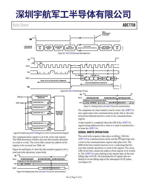
Data SheetADE7758MCU04443-086Figure 87. ADE7758 Interrupt Management04443-087Figure 88. ADE7758Interrupt TimingDINDOUT04443-088Figure 89. Addressing ADE7758 Registers via the Communications RegisterThe communications register is an 8-bit, write-only register. The MSB determines whether the next data transfer operation is a read or a write. The seven LSBs contain the address of the register to be accessed (see Table 16).Figure 90 and Figure 91 show the data transfer sequences for a read and write operation, respectively.MULTIBYTEDIN SCLKDOUTREAD DATACS 04443-089Figure 90. Reading Data from the ADE7758 via the Serial InterfaceDINSCLKCS04443-090Figure 91. Writing Data to the ADE7758 via the Serial InterfaceOn completion of a data transfer (read or write), the ADE7758 once again enters into communications mode, that is, the next instruction followed must be a write to the communications register.A data transfer is completed when the LSB of the ADE7758 register being addressed (for a write or a read) is transferred to or from the ADE7758.SERIAL WRITE OPERATIONThe serial write sequence takes place as follows. With theADE7758 in communications mode and the CS input logic low, a write to the communications register takes place first. The MSB of this byte transfer must be set to 1, indicating that the next data transfer operation is a write to the register. The seven LSBs of this byte contain the address of the register to be written to. The starts shifting in the register data on the next falling edge of SCLK. All remaining bits of register data are shifted in on the falling edge of the subsequent SCLK pulses (see ).ADE7758Figure 92As explained earlier, the data write is initiated by a write to the communications register followed by the data. During a data write operation to the ADE7758, data is transferred to all on-chip registers one byte at a time. After a byte is transferred into the serial port, there is a finite time duration before the content in the serial port buffer is transferred to one of the ADE7758 on-chip registers. Although another byte transfer to the serial port can start while the previous byte is being transferred to the destination register, this second-byte transfer should not finish until at least 900 ns after the end of the previous byte transfer. This functionality is expressed in the timing specification t 6 (see Figure 92). If a write operation is aborted during a byte transfer (CS brought high), then that byte is not written to the destination register.Destination registers can be up to 3 bytes wide (see theAccessing the On-Chip Registers section). Therefore, the first byte shifted into the serial port at DIN is transferred to the most significant byte (MSB) of the destination register. If the destination register is 12 bits wide, for example, a two-byte data transfer must take place. The data is always assumed to be right justified; therefore, in this case, the four MSBs of the first byte would be ignored, and the four LSBs of the first byte written to the ADE7758 would be the four MSBs of the 12-bit word. Figure 93 illustrates this example.COMMAND BYTE MOST SIGNIFICANT BYTE LEAST SIGNIFICANT BYTE04443-091Figure 92. Serial Interface Write Timing DiagramSCLKDIN X X X X DB11DB10DB9DB8DB7DB6DB5DB4DB3DB2DB1DB0MOST SIGNIFICANT BYTE LEAST SIGNIFICANT BYTE04443-092Figure 93. 12-Bit Serial Write OperationSCLKCSDINDOUTCOMMAND BYTE04443-093Figure 94. Serial Interface Read Timing DiagramOPERATIONAL MODE REGISTER (0x13)The general configuration of the ADE7758 is defined by writing to the OPMODE register. Table 18 summarizes the functionality of each bit in the OPMODE register.Table 18. OPMODE RegisterBit Location BitMnemonicDefaultValue Description0 DISHPF 0 The HPFs in all current channel inputs are disabled when this bit is set.1 DISLPF 0 The LPFs after the watt and VAR multipliers are disabled when this bit is set.2 DISCF 1 The frequency outputs APCF and VARCF are disabled when this bit is set.3 to 5 DISMOD 0 By setting these bits, the ADE7758 ADCs can be turned off. In normal operation, these bits shouldbe left at Logic 0.DISMOD[2:0] Description0 0 0 Normal operation.1Redirect the voltage inputs to the signal paths for the current channels andthe current inputs to the signal paths for the voltage channels.0 0 1 Switch off only the current channel ADCs.11Switch off current channel ADCs and redirect the current input signals to thevoltage channel signal paths.0 1 0 Switch off only the voltage channel ADCs.11Switch off voltage channel ADCs and redirect the voltage input signals to thecurrent channel signal paths.11PuttheADE7758 in sleep mode.111PuttheADE7758 in power-down mode (reduces AI DD to 1 mA typ).6 SWRST 0 Software Chip Reset. A data transfer to the ADE7758 should not take place for at least 166 μs aftera software reset.7 Reserved 0 This should be left at 0.MEASUREMENT MODE REGISTER (0x14)The configuration of the PERIOD and peak measurements made by the ADE7758 is defined by writing to the MMODE register. Table 19 summarizes the functionality of each bit in the MMODE register.Table 19. MMODE RegisterBit Location BitMnemonicDefaultValue Description0 to 1 FREQSEL 0 These bits are used to select the source of the measurement of the voltage line frequency.FREQSEL1 FREQSEL0 Source0 0 Phase A0 1 Phase B1 0 Phase C1 1 Reserved2 to 4 PEAKSEL 7 These bits select the phases used for the voltage and current peak registers. Setting Bit 2 switchesthe IPEAK and VPEAK registers to hold the absolute values of the largest current and voltagewaveform (over a fixed number of half-line cycles) from Phase A. The number of half-line cycles isdetermined by the content of the LINECYC register. At the end of the LINECYC number of half-linecycles, the content of the registers is replaced with the new peak values. Similarly, setting Bit 3 turnson the peak detection for Phase B, and Bit 4 for Phase C. Note that if more than one bit is set, theVPEAK and IPEAK registers can hold values from two different phases, that is, the voltage andcurrent peak are independently processed (see the Peak Current Detection section).5 to 7 PKIRQSEL 7 These bits select the phases used for the peak interrupt detection. Setting Bit 5 switches on themonitoring of the absolute current and voltage waveform to Phase A. Similarly, setting Bit 6 turns onthe waveform detection for Phase B, and Bit 7 for Phase C. Note that more than one bit can be set fordetection on multiple phases. If the absolute values of the voltage or current waveform samples inthe selected phases exceeds the preset level specified in the VPINTLVL or IPINTLVL registers thecorresponding bit(s) in the STATUS registers are set (see the Peak Current Detection section).Data Sheet ADE7758ADE7758 Data SheetCOMPUTATIONAL MODE REGISTER (0x16)The computational method of the ADE7758 is defined by writing to the COMPMODE register. Table 21 summarizes the functionality of each bit in the COMPMODE register.。
sp485中文资料_数据手册_参数

VOUT = HIGH
35
VOUT = LOW
35
SP481/SP485 DRIVER
AC Characteristics
Maximum Data Rate
5
Driver Input to Output
Driver Input to Output
Driver Skew
Driver Rise or Fall Time
PARAMETERS
MIN.
SP481/SP485 RECEIVER
AC Characteristics
Maximum Data Rate
5
Receiver Input to Output
60
Receiver Input to Output
60
Diff. Receiver Skew ItPLH-tPHLI
-7V ≤ VO ≤ +12V -7V ≤ VO ≤ +12V
Mbps ns
ns
ns
ns
ns ns ns ns
RE = 5V, DE = 5V
tPLH; RDIFF = 54Ω, CL1 = CL2 = 100pF; see figures 3 and 6
tPHL; RDIFF = 54Ω, CL1 = CL2 = 100pF; see figures 3 and 6 see figures 3 and 6,
Rev. 07/28/04
SP481/483/485 Low Power Half-Duplex RS485 Transceivers
2
© Copyright 2002 Sipex Corporation
TMIN to TMAX and VCC = 5V ± 5% unless otherwise noted.
MAX3085EESA用于RS-485通信低功耗收发器—深圳天高微
器械、瓦斯关联器械、车辆器械、航空器械及车载器械等对人体产生影响的器械 或装置部件使用。 尽管本公司一向致力于提高质量与可靠性,但是半导体产品有可能按照某种概率发生故 障或错误工作。为防止因故障或错误动作而产生人身事故、火灾事故、社会性损害等, 请充分留心冗余设计、火势蔓延对策设计、防止错误动作设计等安全设计。
8 脚塑封 DIP (+70°C 以上 -9.08mW/°C)........……………….…......… …………......... 725mW 8 脚 SO (+70°C 以上 -5.85mW/°C)...............…………….…............……………….…. 470mW 存贮温度范围.............................................................……….……….......…..... -65°C 至+160°C 工作温度范围.............................................................………………..…....…...... -40°C 至+85°C 焊锡温度(10 秒)...…….................................................…………………...….....……………..... +300°C
驱动开启到输出为 tZL 低
图 6,图 10,CL=100pF, S1 关闭
MAX31855热电偶芯片的中文翻译

MAX3855冷端补偿热电偶至数字输出转换器概述MAX31855具有冷端补偿,将K、J、N、T或E型热电偶信号转换成数字量(如果使用S和R 型热电偶,请联系工厂)。
器件输出14位带符号数据,通过SPI TM 兼容接口、以只读格式输出。
转换器的温度分辨率为0.25℃,最高温度读数为+1800℃,最低温度读数为-270℃,对于K型热电偶,温度范围为-200℃至+700℃,保持±2℃精度。
对于整个量程范围的精度及其它类型的热电偶,请参考ThermalCharacteristics 规格。
应用工业电器设备HVAC 汽车特性S 冷端补偿S 14位、0.25℃分辨率S 提供K、J、N、T和E型热电偶器件版本(如果使用S和R型热电偶,请联系工厂) (见表1) S 简单的SPI兼容接口(只读)S 检测热电偶对GND或V CC 短路S 检测热电偶开路典型应用电路SPI是Motorola,Inc.的商标。
对于价格,供货及订购信息,请联络Maxim在1-888-629-4642,或访问Maxim的网站。
绝对最大额定值范围电源电压范围(VCC和GND)..................-0.3V to +4.0V所有其他引脚............................................-0.3V到(V CC+ 0.3V)连续功率耗散(T A =+70℃)SO(减免5.9mW/ ℃以上+70℃).......................470.6mWESD保护(所有引脚,人体模型).............±2000kV工作温度范围........................-40℃至+125°C连接点温度................................................ .....+150°C存储温度范围..........................-65℃至+150°清除温度(焊接,10秒) (300)焊接温度(回流) (260)强调超出“绝对最大额定值”,即可能对器件造成永久性损坏。
ADXL335BCPZ-RL7数据表PDF,功能介绍说明

ADXL335BCPZ-RL7数据表PDF,功能介绍说明
ADXL335是一款小尺寸、薄型、低功耗、完整的三轴加速度计,提供经过信号调理的电压输出,该产品的满量程加速度测量范围为±3 g(最小值),可以测量倾斜检测应用中的静态重力加速度,以及运动、冲击或振动导致的动态加速度。
特征
三轴检测
小尺寸、薄型封装
4 mm × 4 mm × 1.4
5 mm LFCSP
低功耗:350 μA(典型值)
单电源供电:1.8 V to 3.6 V
抗冲击能力:10,000 g
出色的温度稳定性
通过各轴的一个电容调整相应的带宽
符合RoHS/WEEE无铅要求
(亚德诺半导体)传感器解决方案包括 MEMS 加速度计、MEMS 陀螺仪、MEMS 惯性测量单元(IMUs)、光学传感器、各向异性磁阻(AMR)传感器、温度传感器、霍尔效应传感器。
高性能分立原件和即插即用的解决方案能够高效可靠地应对复杂的设计要求。
应用
低功耗、运动和倾斜感应应用
移动设备
游戏系统
磁盘驱动器保护
图像稳定
运动和健康设备
注:本文部分内容与图片来源于网络,版权归原作者所有。
如有侵权,请联系删除!。
MAX485CPA+中文资料
For pricing, delivery, and ordering information,please contact Maxim/Dallas Direct!at 1-888-629-4642, or visit Maxim’s website at .General DescriptionThe MAX481, MAX483, MAX485, MAX487–MAX491, and MAX1487 are low-power transceivers for RS-485 and RS-422 communication. Each part contains one driver and one receiver. The MAX483, MAX487, MAX488, and MAX489feature reduced slew-rate drivers that minimize EMI and reduce reflections caused by improperly terminated cables,thus allowing error-free data transmission up to 250kbps.The driver slew rates of the MAX481, MAX485, MAX490,MAX491, and MAX1487 are not limited, allowing them to transmit up to 2.5Mbps.These transceivers draw between 120µA and 500µA of supply current when unloaded or fully loaded with disabled drivers. Additionally, the MAX481, MAX483, and MAX487have a low-current shutdown mode in which they consume only 0.1µA. All parts operate from a single 5V supply.Drivers are short-circuit current limited and are protected against excessive power dissipation by thermal shutdown circuitry that places the driver outputs into a high-imped-ance state. The receiver input has a fail-safe feature that guarantees a logic-high output if the input is open circuit.The MAX487 and MAX1487 feature quarter-unit-load receiver input impedance, allowing up to 128 MAX487/MAX1487 transceivers on the bus. Full-duplex communi-cations are obtained using the MAX488–MAX491, while the MAX481, MAX483, MAX485, MAX487, and MAX1487are designed for half-duplex applications.________________________ApplicationsLow-Power RS-485 Transceivers Low-Power RS-422 Transceivers Level TranslatorsTransceivers for EMI-Sensitive Applications Industrial-Control Local Area Networks__Next Generation Device Features♦For Fault-Tolerant ApplicationsMAX3430: ±80V Fault-Protected, Fail-Safe, 1/4Unit Load, +3.3V, RS-485 TransceiverMAX3440E–MAX3444E: ±15kV ESD-Protected,±60V Fault-Protected, 10Mbps, Fail-Safe, RS-485/J1708 Transceivers♦For Space-Constrained ApplicationsMAX3460–MAX3464: +5V, Fail-Safe, 20Mbps,Profibus RS-485/RS-422 TransceiversMAX3362: +3.3V, High-Speed, RS-485/RS-422Transceiver in a SOT23 PackageMAX3280E–MAX3284E: ±15kV ESD-Protected,52Mbps, +3V to +5.5V, SOT23, RS-485/RS-422,True Fail-Safe ReceiversMAX3293/MAX3294/MAX3295: 20Mbps, +3.3V,SOT23, RS-855/RS-422 Transmitters ♦For Multiple Transceiver ApplicationsMAX3030E–MAX3033E: ±15kV ESD-Protected,+3.3V, Quad RS-422 Transmitters ♦For Fail-Safe ApplicationsMAX3080–MAX3089: Fail-Safe, High-Speed (10Mbps), Slew-Rate-Limited RS-485/RS-422Transceivers♦For Low-Voltage ApplicationsMAX3483E/MAX3485E/MAX3486E/MAX3488E/MAX3490E/MAX3491E: +3.3V Powered, ±15kV ESD-Protected, 12Mbps, Slew-Rate-Limited,True RS-485/RS-422 TransceiversMAX481/MAX483/MAX485/MAX487–MAX491/MAX1487Low-Power, Slew-Rate-Limited RS-485/RS-422 Transceivers______________________________________________________________Selection Table19-0122; Rev 8; 10/03Ordering Information appears at end of data sheet.M A X 481/M A X 483/M A X 485/M A X 487–M A X 491/M A X 1487Low-Power, Slew-Rate-Limited RS-485/RS-422 Transceivers 2_______________________________________________________________________________________ABSOLUTE MAXIMUM RATINGSSupply Voltage (V CC ).............................................................12V Control Input Voltage (RE , DE)...................-0.5V to (V CC + 0.5V)Driver Input Voltage (DI).............................-0.5V to (V CC + 0.5V)Driver Output Voltage (A, B)...................................-8V to +12.5V Receiver Input Voltage (A, B).................................-8V to +12.5V Receiver Output Voltage (RO).....................-0.5V to (V CC +0.5V)Continuous Power Dissipation (T A = +70°C)8-Pin Plastic DIP (derate 9.09mW/°C above +70°C)....727mW 14-Pin Plastic DIP (derate 10.00mW/°C above +70°C)..800mW 8-Pin SO (derate 5.88mW/°C above +70°C).................471mW14-Pin SO (derate 8.33mW/°C above +70°C)...............667mW 8-Pin µMAX (derate 4.1mW/°C above +70°C)..............830mW 8-Pin CERDIP (derate 8.00mW/°C above +70°C).........640mW 14-Pin CERDIP (derate 9.09mW/°C above +70°C).......727mW Operating Temperature RangesMAX4_ _C_ _/MAX1487C_ A...............................0°C to +70°C MAX4__E_ _/MAX1487E_ A.............................-40°C to +85°C MAX4__MJ_/MAX1487MJA...........................-55°C to +125°C Storage Temperature Range.............................-65°C to +160°C Lead Temperature (soldering, 10sec).............................+300°CDC ELECTRICAL CHARACTERISTICS(V CC = 5V ±5%, T A = T MIN to T MAX , unless otherwise noted.) (Notes 1, 2)Stresses beyond those listed under “Absolute Maximum Ratings” may cause permanent damage to the device. These are stress ratings only, and functional operation of the device at these or any other conditions beyond those indicated in the operational sections of the specifications is not implied. Exposure to absolute maximum rating conditions for extended periods may affect device reliability.V V IN = -7VV IN = 12V V IN = -7V V IN = 12V Input Current (A, B)I IN2V TH k Ω48-7V ≤V CM ≤12V, MAX487/MAX1487R INReceiver Input Resistance -7V ≤V CM ≤12V, all devices except MAX487/MAX1487R = 27Ω(RS-485), Figure 40.4V ≤V O ≤2.4VR = 50Ω(RS-422)I O = 4mA, V ID = -200mV I O = -4mA, V ID = 200mV V CM = 0V-7V ≤V CM ≤12V DE, DI, RE DE, DI, RE MAX487/MAX1487,DE = 0V, V CC = 0V or 5.25VDE, DI, RE R = 27Ωor 50Ω, Figure 4R = 27Ωor 50Ω, Figure 4R = 27Ωor 50Ω, Figure 4DE = 0V;V CC = 0V or 5.25V,all devices except MAX487/MAX1487CONDITIONSk Ω12µA ±1I OZRThree-State (high impedance)Output Current at ReceiverV 0.4V OL Receiver Output Low Voltage 3.5V OH Receiver Output High Voltage mV 70∆V TH Receiver Input Hysteresis V -0.20.2Receiver Differential Threshold Voltage-0.2mA 0.25mA-0.81.01.55V OD2Differential Driver Output (with load)V 2V 5V OD1Differential Driver Output (no load)µA±2I IN1Input CurrentV 0.8V IL Input Low Voltage V 2.0V IH Input High Voltage V 0.2∆V OD Change in Magnitude of Driver Common-Mode Output Voltage for Complementary Output States V 0.2∆V OD Change in Magnitude of Driver Differential Output Voltage for Complementary Output States V 3V OC Driver Common-Mode Output VoltageUNITS MINTYPMAX SYMBOL PARAMETERMAX481/MAX483/MAX485/MAX487–MAX491/MAX1487Low-Power, Slew-Rate-Limited RS-485/RS-422 Transceivers_______________________________________________________________________________________3SWITCHING CHARACTERISTICS—MAX481/MAX485, MAX490/MAX491, MAX1487(V CC = 5V ±5%, T A = T MIN to T MAX , unless otherwise noted.) (Notes 1, 2)DC ELECTRICAL CHARACTERISTICS (continued)(V CC = 5V ±5%, T A = T MIN to T MAX , unless otherwise noted.) (Notes 1, 2)ns 103060t PHLDriver Rise or Fall Time Figures 6 and 8, R DIFF = 54Ω, C L1= C L2= 100pF ns MAX490M, MAX491M MAX490C/E, MAX491C/E2090150MAX481, MAX485, MAX1487MAX490M, MAX491MMAX490C/E, MAX491C/E MAX481, MAX485, MAX1487Figures 6 and 8, R DIFF = 54Ω,C L1= C L2= 100pF MAX481 (Note 5)Figures 5 and 11, C RL = 15pF, S2 closedFigures 5 and 11, C RL = 15pF, S1 closed Figures 5 and 11, C RL = 15pF, S2 closed Figures 5 and 11, C RL = 15pF, S1 closed Figures 6 and 10, R DIFF = 54Ω,C L1= C L2= 100pFFigures 6 and 8,R DIFF = 54Ω,C L1= C L2= 100pF Figures 6 and 10,R DIFF = 54Ω,C L1= C L2= 100pF CONDITIONS ns 510t SKEW ns50200600t SHDNTime to ShutdownMbps 2.5f MAX Maximum Data Rate ns 2050t HZ Receiver Disable Time from High ns 103060t PLH 2050t LZ Receiver Disable Time from Low ns 2050t ZH Driver Input to Output Receiver Enable to Output High ns 2050t ZL Receiver Enable to Output Low 2090200ns ns 134070t HZ t SKD Driver Disable Time from High |t PLH - t PHL |DifferentialReceiver Skewns 4070t LZ Driver Disable Time from Low ns 4070t ZL Driver Enable to Output Low 31540ns51525ns 31540t R , t F 2090200Driver Output Skew to Output t PLH , t PHL Receiver Input to Output4070t ZH Driver Enable to Output High UNITS MIN TYP MAX SYMBOL PARAMETERFigures 7 and 9, C L = 100pF, S2 closed Figures 7 and 9, C L = 100pF, S1 closed Figures 7 and 9, C L = 15pF, S1 closed Figures 7 and 9, C L = 15pF, S2 closedM A X 481/M A X 483/M A X 485/M A X 487–M A X 491/M A X 1487Low-Power, Slew-Rate-Limited RS-485/RS-422 Transceivers 4_______________________________________________________________________________________SWITCHING CHARACTERISTICS—MAX483, MAX487/MAX488/MAX489(V CC = 5V ±5%, T A = T MIN to T MAX , unless otherwise noted.) (Notes 1, 2)SWITCHING CHARACTERISTICS—MAX481/MAX485, MAX490/MAX491, MAX1487 (continued)(V CC = 5V ±5%, T A = T MIN to T MAX , unless otherwise noted.) (Notes 1, 2)3001000Figures 7 and 9, C L = 100pF, S2 closed Figures 7 and 9, C L = 100pF, S1 closed Figures 5 and 11, C L = 15pF, S2 closed,A - B = 2VCONDITIONSns 40100t ZH(SHDN)Driver Enable from Shutdown toOutput High (MAX481)nsFigures 5 and 11, C L = 15pF, S1 closed,B - A = 2Vt ZL(SHDN)Receiver Enable from Shutdownto Output Low (MAX481)ns 40100t ZL(SHDN)Driver Enable from Shutdown toOutput Low (MAX481)ns 3001000t ZH(SHDN)Receiver Enable from Shutdownto Output High (MAX481)UNITS MINTYP MAX SYMBOLPARAMETERt PLH t SKEW Figures 6 and 8, R DIFF = 54Ω,C L1= C L2= 100pFt PHL Figures 6 and 8, R DIFF = 54Ω,C L1= C L2= 100pFDriver Input to Output Driver Output Skew to Output ns 100800ns ns 2000MAX483/MAX487, Figures 7 and 9,C L = 100pF, S2 closedt ZH(SHDN)Driver Enable from Shutdown to Output High2502000ns2500MAX483/MAX487, Figures 5 and 11,C L = 15pF, S1 closedt ZL(SHDN)Receiver Enable from Shutdown to Output Lowns 2500MAX483/MAX487, Figures 5 and 11,C L = 15pF, S2 closedt ZH(SHDN)Receiver Enable from Shutdown to Output Highns 2000MAX483/MAX487, Figures 7 and 9,C L = 100pF, S1 closedt ZL(SHDN)Driver Enable from Shutdown to Output Lowns 50200600MAX483/MAX487 (Note 5) t SHDN Time to Shutdownt PHL t PLH , t PHL < 50% of data period Figures 5 and 11, C RL = 15pF, S2 closed Figures 5 and 11, C RL = 15pF, S1 closed Figures 5 and 11, C RL = 15pF, S2 closed Figures 5 and 11, C RL = 15pF, S1 closed Figures 7 and 9, C L = 15pF, S2 closed Figures 6 and 10, R DIFF = 54Ω,C L1= C L2= 100pFFigures 7 and 9, C L = 15pF, S1 closed Figures 7 and 9, C L = 100pF, S1 closed Figures 7 and 9, C L = 100pF, S2 closed CONDITIONSkbps 250f MAX 2508002000Maximum Data Rate ns 2050t HZ Receiver Disable Time from High ns 25080020002050t LZ Receiver Disable Time from Low ns 2050t ZH Receiver Enable to Output High ns 2050t ZL Receiver Enable to Output Low ns ns 1003003000t HZ t SKD Driver Disable Time from High I t PLH - t PHL I DifferentialReceiver SkewFigures 6 and 10, R DIFF = 54Ω,C L1= C L2= 100pFns 3003000t LZ Driver Disable Time from Low ns 2502000t ZL Driver Enable to Output Low ns Figures 6 and 8, R DIFF = 54Ω,C L1= C L2= 100pFns 2502000t R , t F 2502000Driver Rise or Fall Time ns t PLH Receiver Input to Output2502000t ZH Driver Enable to Output High UNITS MIN TYP MAX SYMBOL PARAMETERMAX481/MAX483/MAX485/MAX487–MAX491/MAX1487Low-Power, Slew-Rate-Limited RS-485/RS-422 Transceivers_______________________________________________________________________________________530002.5OUTPUT CURRENT vs.RECEIVER OUTPUT LOW VOLTAGE525M A X 481-01OUTPUT LOW VOLTAGE (V)O U T P U T C U R R E N T (m A )1.515100.51.02.0203540450.90.1-50-252575RECEIVER OUTPUT LOW VOLTAGE vs.TEMPERATURE0.30.7TEMPERATURE (°C)O U T P U TL O W V O L T A G E (V )500.50.80.20.60.40100125-20-41.5 2.0 3.0 5.0OUTPUT CURRENT vs.RECEIVER OUTPUT HIGH VOLTAGE-8-16M A X 481-02OUTPUT HIGH VOLTAGE (V)O U T P U T C U R R E N T (m A )2.5 4.0-12-18-6-14-10-203.54.5 4.83.2-50-252575RECEIVER OUTPUT HIGH VOLTAGE vs.TEMPERATURE3.64.4TEMPERATURE (°C)O U T P UT H I G H V O L T A G E (V )0504.04.63.44.23.83.01001259000 1.0 3.0 4.5DRIVER OUTPUT CURRENT vs.DIFFERENTIAL OUTPUT VOLTAGE1070M A X 481-05DIFFERENTIAL OUTPUT VOLTAGE (V)O U T P U T C U R R E N T (m A )2.0 4.05030806040200.5 1.5 2.53.5 2.31.5-50-2525125DRIVER DIFFERENTIAL OUTPUT VOLTAGEvs. TEMPERATURE1.72.1TEMPERATURE (°C)D I F FE R E N T I A L O U T P U T V O L T A G E (V )751.92.21.62.01.8100502.4__________________________________________Typical Operating Characteristics(V CC = 5V, T A = +25°C, unless otherwise noted.)NOTES FOR ELECTRICAL/SWITCHING CHARACTERISTICSNote 1:All currents into device pins are positive; all currents out of device pins are negative. All voltages are referenced to deviceground unless otherwise specified.Note 2:All typical specifications are given for V CC = 5V and T A = +25°C.Note 3:Supply current specification is valid for loaded transmitters when DE = 0V.Note 4:Applies to peak current. See Typical Operating Characteristics.Note 5:The MAX481/MAX483/MAX487 are put into shutdown by bringing RE high and DE low. If the inputs are in this state for lessthan 50ns, the parts are guaranteed not to enter shutdown. If the inputs are in this state for at least 600ns, the parts are guaranteed to have entered shutdown. See Low-Power Shutdown Mode section.M A X 481/M A X 483/M A X 485/M A X 487–M A X 491/M A X 1487Low-Power, Slew-Rate-Limited RS-485/RS-422 Transceivers 6___________________________________________________________________________________________________________________Typical Operating Characteristics (continued)(V CC = 5V, T A = +25°C, unless otherwise noted.)120008OUTPUT CURRENT vs.DRIVER OUTPUT LOW VOLTAGE20100M A X 481-07OUTPUT LOW VOLTAGE (V)O U T P U T C U R R E N T (m A )6604024801012140-1200-7-5-15OUTPUT CURRENT vs.DRIVER OUTPUT HIGH VOLTAGE-20-80M A X 481-08OUTPUT HIGH VOLTAGE (V)O U T P U T C U R R E N T (m A )-31-603-6-4-2024-100-40100-40-60-2040100120MAX1487SUPPLY CURRENT vs. TEMPERATURE300TEMPERATURE (°C)S U P P L Y C U R R E N T (µA )20608050020060040000140100-50-2550100MAX481/MAX485/MAX490/MAX491SUPPLY CURRENT vs. TEMPERATURE300TEMPERATURE (°C)S U P P L Y C U R R E N T (µA )257550020060040000125100-50-2550100MAX483/MAX487–MAX489SUPPLY CURRENT vs. TEMPERATURE300TEMPERATURE (°C)S U P P L Y C U R R E N T (µA )257550020060040000125MAX481/MAX483/MAX485/MAX487–MAX491/MAX1487Low-Power, Slew-Rate-Limited RS-485/RS-422 Transceivers_______________________________________________________________________________________7______________________________________________________________Pin DescriptionFigure 1. MAX481/MAX483/MAX485/MAX487/MAX1487 Pin Configuration and Typical Operating CircuitM A X 481/M A X 483/M A X 485/M A X 487–M A X 491/M A X 1487__________Applications InformationThe MAX481/MAX483/MAX485/MAX487–MAX491 and MAX1487 are low-power transceivers for RS-485 and RS-422 communications. The MAX481, MAX485, MAX490,MAX491, and MAX1487 can transmit and receive at data rates up to 2.5Mbps, while the MAX483, MAX487,MAX488, and MAX489 are specified for data rates up to 250kbps. The MAX488–MAX491 are full-duplex trans-ceivers while the MAX481, MAX483, MAX485, MAX487,and MAX1487 are half-duplex. In addition, Driver Enable (DE) and Receiver Enable (RE) pins are included on the MAX481, MAX483, MAX485, MAX487, MAX489,MAX491, and MAX1487. When disabled, the driver and receiver outputs are high impedance.MAX487/MAX1487:128 Transceivers on the BusThe 48k Ω, 1/4-unit-load receiver input impedance of the MAX487 and MAX1487 allows up to 128 transceivers on a bus, compared to the 1-unit load (12k Ωinput impedance) of standard RS-485 drivers (32 trans-ceivers maximum). Any combination of MAX487/MAX1487 and other RS-485 transceivers with a total of 32 unit loads or less can be put on the bus. The MAX481/MAX483/MAX485 and MAX488–MAX491 have standard 12k ΩReceiver Input impedance.Low-Power, Slew-Rate-Limited RS-485/RS-422 Transceivers 8_______________________________________________________________________________________Figure 2. MAX488/MAX490 Pin Configuration and Typical Operating CircuitFigure 3. MAX489/MAX491 Pin Configuration and Typical Operating CircuitMAX483/MAX487/MAX488/MAX489:Reduced EMI and ReflectionsThe MAX483 and MAX487–MAX489 are slew-rate limit-ed, minimizing EMI and reducing reflections caused by improperly terminated cables. Figure 12 shows the dri-ver output waveform and its Fourier analysis of a 150kHz signal transmitted by a MAX481, MAX485,MAX490, MAX491, or MAX1487. High-frequency har-monics with large amplitudes are evident. Figure 13shows the same information displayed for a MAX483,MAX487, MAX488, or MAX489 transmitting under the same conditions. Figure 13’s high-frequency harmonics have much lower amplitudes, and the potential for EMI is significantly reduced.MAX481/MAX483/MAX485/MAX487–MAX491/MAX1487Low-Power, Slew-Rate-Limited RS-485/RS-422 Transceivers_______________________________________________________________________________________9_________________________________________________________________Test CircuitsFigure 4. Driver DC Test Load Figure 5. Receiver Timing Test LoadFigure 6. Driver/Receiver Timing Test Circuit Figure 7. Driver Timing Test LoadM A X 481/M A X 483/M A X 485/M A X 487–M A X 491/M A X 1487Low-Power, Slew-Rate-Limited RS-485/RS-422 Transceivers 10_______________________________________________________Switching Waveforms_________________Function Tables (MAX481/MAX483/MAX485/MAX487/MAX1487)Figure 8. Driver Propagation DelaysFigure 9. Driver Enable and Disable Times (except MAX488 and MAX490)Figure 10. Receiver Propagation DelaysFigure 11. Receiver Enable and Disable Times (except MAX488and MAX490)Table 1. TransmittingTable 2. ReceivingLow-Power Shutdown Mode (MAX481/MAX483/MAX487)A low-power shutdown mode is initiated by bringing both RE high and DE low. The devices will not shut down unless both the driver and receiver are disabled.In shutdown, the devices typically draw only 0.1µA of supply current.RE and DE may be driven simultaneously; the parts are guaranteed not to enter shutdown if RE is high and DE is low for less than 50ns. If the inputs are in this state for at least 600ns, the parts are guaranteed to enter shutdown.For the MAX481, MAX483, and MAX487, the t ZH and t ZL enable times assume the part was not in the low-power shutdown state (the MAX485/MAX488–MAX491and MAX1487 can not be shut down). The t ZH(SHDN)and t ZL(SHDN)enable times assume the parts were shut down (see Electrical Characteristics ).It takes the drivers and receivers longer to become enabled from the low-power shutdown state (t ZH(SHDN ), t ZL(SHDN)) than from the operating mode (t ZH , t ZL ). (The parts are in operating mode if the –R —E –,DE inputs equal a logical 0,1 or 1,1 or 0, 0.)Driver Output ProtectionExcessive output current and power dissipation caused by faults or by bus contention are prevented by two mechanisms. A foldback current limit on the output stage provides immediate protection against short cir-cuits over the whole common-mode voltage range (see Typical Operating Characteristics ). In addition, a ther-mal shutdown circuit forces the driver outputs into a high-impedance state if the die temperature rises excessively.Propagation DelayMany digital encoding schemes depend on the differ-ence between the driver and receiver propagation delay times. Typical propagation delays are shown in Figures 15–18 using Figure 14’s test circuit.The difference in receiver delay times, | t PLH - t PHL |, is typically under 13ns for the MAX481, MAX485,MAX490, MAX491, and MAX1487 and is typically less than 100ns for the MAX483 and MAX487–MAX489.The driver skew times are typically 5ns (10ns max) for the MAX481, MAX485, MAX490, MAX491, and MAX1487, and are typically 100ns (800ns max) for the MAX483 and MAX487–MAX489.MAX481/MAX483/MAX485/MAX487–MAX491/MAX1487Low-Power, Slew-Rate-Limited RS-485/RS-422 Transceivers______________________________________________________________________________________1110dB/div0Hz5MHz500kHz/div10dB/div0Hz5MHz500kHz/divFigure 12. Driver Output Waveform and FFT Plot of MAX481/MAX485/MAX490/MAX491/MAX1487 Transmitting a 150kHz SignalFigure 13. Driver Output Waveform and FFT Plot of MAX483/MAX487–MAX489 Transmitting a 150kHz SignalM A X 481/M A X 483/M A X 485/M A X 487–M A X 491/M A X 1487Low-Power, Slew-Rate-Limited RS-485/RS-422 Transceivers 12______________________________________________________________________________________V CC = 5V T A = +25°CV CC = 5V T A = +25°CV CC = 5V T A = +25°CV CC = 5V T A = +25°CFigure 14. Receiver Propagation Delay Test CircuitFigure 15. MAX481/MAX485/MAX490/MAX491/MAX1487Receiver t PHLFigure 16. MAX481/MAX485/MAX490/MAX491/MAX1487Receiver t PLHPHL Figure 18. MAX483, MAX487–MAX489 Receiver t PLHLine Length vs. Data RateThe RS-485/RS-422 standard covers line lengths up to 4000 feet. For line lengths greater than 4000 feet, see Figure 23.Figures 19 and 20 show the system differential voltage for the parts driving 4000 feet of 26AWG twisted-pair wire at 110kHz into 120Ωloads.Typical ApplicationsThe MAX481, MAX483, MAX485, MAX487–MAX491, and MAX1487 transceivers are designed for bidirectional data communications on multipoint bus transmission lines.Figures 21 and 22 show typical network applications circuits. These parts can also be used as line repeaters, with cable lengths longer than 4000 feet, as shown in Figure 23.To minimize reflections, the line should be terminated at both ends in its characteristic impedance, and stub lengths off the main line should be kept as short as possi-ble. The slew-rate-limited MAX483 and MAX487–MAX489are more tolerant of imperfect termination.MAX481/MAX483/MAX485/MAX487–MAX491/MAX1487Low-Power, Slew-Rate-Limited RS-485/RS-422 Transceivers______________________________________________________________________________________13DIV Y -V ZRO5V 0V1V0V -1V5V 0V2µs/divFigure 19. MAX481/MAX485/MAX490/MAX491/MAX1487 System Differential Voltage at 110kHz Driving 4000ft of Cable Figure 20. MAX483, MAX487–MAX489 System Differential Voltage at 110kHz Driving 4000ft of CableFigure 21. MAX481/MAX483/MAX485/MAX487/MAX1487 Typical Half-Duplex RS-485 NetworkM A X 481/M A X 483/M A X 485/M A X 487–M A X 491/M A X 1487Low-Power, Slew-Rate-Limited RS-485/RS-422 Transceivers 14______________________________________________________________________________________Figure 22. MAX488–MAX491 Full-Duplex RS-485 NetworkFigure 23. Line Repeater for MAX488–MAX491Isolated RS-485For isolated RS-485 applications, see the MAX253 and MAX1480 data sheets.MAX481/MAX483/MAX485/MAX487–MAX491/MAX1487Low-Power, Slew-Rate-Limited RS-485/RS-422 Transceivers______________________________________________________________________________________15_______________Ordering Information_________________Chip TopographiesMAX481/MAX483/MAX485/MAX487/MAX1487N.C. RO 0.054"(1.372mm)0.080"(2.032mm)DE DIGND B N.C.V CCARE * Contact factory for dice specifications.__Ordering Information (continued)M A X 481/M A X 483/M A X 485/M A X 487–M A X 491/M A X 1487Low-Power, Slew-Rate-Limited RS-485/RS-422 Transceivers 16______________________________________________________________________________________TRANSISTOR COUNT: 248SUBSTRATE CONNECTED TO GNDMAX488/MAX490B RO 0.054"(1.372mm)0.080"(2.032mm)N.C. DIGND Z A V CCYN.C._____________________________________________Chip Topographies (continued)MAX489/MAX491B RO 0.054"(1.372mm)0.080"(2.032mm)DE DIGND Z A V CCYREMAX481/MAX483/MAX485/MAX487–MAX491/MAX1487Low-Power, Slew-Rate-Limited RS-485/RS-422 Transceivers______________________________________________________________________________________17Package Information(The package drawing(s) in this data sheet may not reflect the most current specifications. For the latest package outline information go to /packages .)S O I C N .E P SM A X 481/M A X 483/M A X 485/M A X 487–M A X 491/M A X 1487Low-Power, Slew-Rate-Limited RS-485/RS-422 Transceivers 18______________________________________________________________________________________Package Information (continued)(The package drawing(s) in this data sheet may not reflect the most current specifications. For the latest package outline information go to /packages .)MAX481/MAX483/MAX485/MAX487–MAX491Low-Power, Slew-Rate-Limited RS-485/RS-422 TransceiversMaxim cannot assume responsibility for use of any circuitry other than circuitry entirely embodied in a Maxim product. No circuit patent licenses are implied. Maxim reserves the right to change the circuitry and specifications without notice at any time.Maxim Integrated Products, 120 San Gabriel Drive, Sunnyvale, CA 94086 408-737-7600 ____________________19©2003 Maxim Integrated ProductsPrinted USAis a registered trademark of Maxim Integrated Products.M A X 481/M A X 483/M A X 485/M A X 487–M A X 491/M A X 1487P D I P N .E PSPackage Information (continued)(The package drawing(s) in this data sheet may not reflect the most current specifications. For the latest package outline information go to /packages .)。
MEMORY存储芯片MAX485EEPA+中文规格书
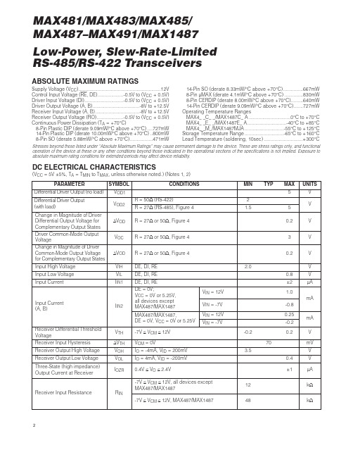
Low-Power, Slew-Rate-Limited RS-485/RS-422 Transceivers2MAX481/MAX483/MAX485/MAX487–MAX491/MAX1487ABSOLUTE MAXIMUM RATINGSSupply Voltage (V CC ) (12V)Control Input Voltage (RE , DE)...................-0.5V to (V CC + 0.5V)Driver Input Voltage (DI).............................-0.5V to (V CC + 0.5V)Driver Output Voltage (A, B)...................................-8V to +12.5VReceiver Input Voltage (A, B).................................-8V to +12.5VReceiver Output Voltage (RO)....................-0.5V to (V CC + 0.5V)Continuous Power Dissipation (T A = +70°C)8-Pin Plastic DIP (derate 9.09mW/°C above +70°C)....727mW14-Pin Plastic DIP (derate 10.00mW/°C above +70°C)..800mW8-Pin SO (derate 5.88mW/°C above +70°C).................471mW 14-Pin SO (derate 8.33mW/°C above +70°C)...............667mW 8-Pin µMAX (derate 4.1mW/°C above +70°C)..............830mW 8-Pin CERDIP (derate 8.00mW/°C above +70°C).........640mW 14-Pin CERDIP (derate 9.09mW/°C above +70°C).......727mW Operating Temperature Ranges MAX4_ _C_ _/MAX1487C_ A...............................0°C to +70°C MAX4__E_ _/MAX1487E_ A.............................-40°C to +85°C MAX4__M_/MAX1487MJA.............................-55°C to +125°C Storage Temperature Range.............................-65°C to +160°C Lead Temperature (soldering, 10sec).............................+300°C DC ELECTRICAL CHARACTERISTICS(V CC = 5V ±5%, T A = T MIN to T MAX , unless otherwise noted.) (Notes 1, 2)Stresses beyond those listed under “Absolute Maximum Ratings” may cause permanent damage to the device. These are stress ratings only, and functional operation of the device at these or any other conditions beyond those indicated in the operational sections of the specifications is not implied. Exposure to absolute maximum rating conditions for extended periods may affect device reliability.V V IN = -7V V IN = 12V V IN = -7V V IN = 12V Input Current (A, B)I IN2V TH k Ω48-7V ≤V CM ≤12V, MAX487/MAX1487R INReceiver Input Resistance -7V ≤V CM ≤12V, all devices exceptMAX487/MAX1487R = 27Ω(RS-485), Figure 40.4V ≤V O ≤2.4VR = 50Ω(RS-422)I O = 4mA, V ID = -200mV I O = -4mA, V ID = 200mV V CM = 0V -7V ≤V CM ≤12V DE, DI, REDE, DI, RE MAX487/MAX1487,DE = 0V, V CC = 0V or 5.25VDE, DI, RE R = 27Ωor 50Ω, Figure 4R = 27Ωor 50Ω, Figure 4R = 27Ωor 50Ω, Figure 4DE = 0V;V CC = 0V or 5.25V,all devices exceptMAX487/MAX1487CONDITIONS k Ω12µA ±1I OZR Three-State (high impedance)Output Current at Receiver V 0.4V OL Receiver Output Low Voltage3.5V OH Receiver Output High VoltagemV 70ΔV TH Receiver Input HysteresisV -0.20.2Receiver Differential ThresholdVoltage-0.2mA 0.25mA -0.81.01.55V OD2Differential Driver Output(with load)V 2V 5V OD1Differential Driver Output (no load)µA ±2I IN1Input Current V 0.8V IL Input Low VoltageV 2.0V IH Input High VoltageV 0.2ΔV OD Change in Magnitude of DriverCommon-Mode Output Voltagefor Complementary Output StatesV 0.2ΔV OD Change in Magnitude of DriverDifferential Output Voltage forComplementary Output StatesV 3V OC Driver Common-Mode OutputVoltageUNITS MIN TYP MAX SYMBOL PARAMETERLow-Power, Slew-Rate-Limited RS-485/RS-422 Transceivers7MAX481/MAX483/MAX485/MAX487–MAX491/MAX1487______________________________________________________________Pin DescriptionFigure 1. MAX481/MAX483/MAX485/MAX487/MAX1487 Pin Configuration and Typical Operating Circuit。
R485CPBB中文资料
Handling Precautions
The R485-Type receiver is manufactured with a 39 in. ± 4 in. (100 cm ± 10 cm) single-mode fiber pigtail with a 900 µm OD PVC outer jacket. Both SC and FCPC connectors are offered on standard versions. Other optical connector options are available on special order. Please contact an Agere Systems Account Manager for availability and ordering information.
s SONET/SDH compatible for OC-48/STM-16 data rate
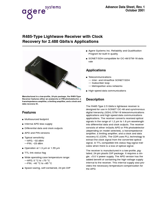
Manufactured in a low-profile, 24-pin package, the R485-Type Receiver features either an avalanche or PIN photodetector, a transimpedance amplifier, a limiting amplifier, and a clock and data recovery IC.
Installation Considerations
Although the receiver has been designed with ruggedness in mind, care should be used during handling. The optical connector should be kept free from dust. The optical connector process cap should be kept in place as a dust cover when the device is not connected to a cable. If contamination is present on the optical connector, the use of canned air with a extension tube should remove any loose debris. Other cleaning procedures are outlined in the Cleaning Fiber Optic Assemblies Technical Note (TN95-010LWP).
- 1、下载文档前请自行甄别文档内容的完整性,平台不提供额外的编辑、内容补充、找答案等附加服务。
- 2、"仅部分预览"的文档,不可在线预览部分如存在完整性等问题,可反馈申请退款(可完整预览的文档不适用该条件!)。
- 3、如文档侵犯您的权益,请联系客服反馈,我们会尽快为您处理(人工客服工作时间:9:00-18:30)。
Single Supply, High Speed, Rail-to-Rail Output, Triple Op Amp
ADA4855-3
Rev. 0 Information furnished by Analog Devices is believed to be accurate and reliable. However, no responsibility is assumed by Analog Devices for its use, nor for any infringements of patents or other rights of third parties that may result from its use. Specifications subject to change without notice. No license is granted by implication or otherwise under any patent or patent rights of Analog Devices. Trademarks and registered trademarks are the property of their respective owners. One Technology Way, P.O. Box 9106, Norwood, MA 02062-9106, U.S.A.Tel: 781.329.4700 www.analog.com Fax: 781.461.3113 ©2008 Analog Devices, Inc. All rights reserved.
FEATURES Voltage feedback architecture Rail-to-rail output swing: 0.1 V to 4.9 V High speed amplifiers 410 MHz, −3 dB bandwidth, G = 1 210 MHz, −3 dB bandwidth, G = 2 Slew rate: 870 V/μs 53 MHz, 0.1 dB large signal flatness 5.3 ns settling time to 0.1% with 2 V step High input common-mode voltage range −VS − 0.2 V to +VS − 1 V Supply range: 3 V to 5.5 V Differential gain error: 0.01% Differential phase error: 0.01° Low power 7.8 mA/amplifier typical supply current Power-down feature Available in 16-lead LFCSP APPLICATIONS Professional video Consumer video Imaging Instrumentation Base stations Active filters CONNECTION DIAGRAM 12+IN2NC
+IN3–IN3
OUT3
–VS
+IN1–IN1OUT1–VS
PDNC3411OUT212+V
S
10–IN29
5678
16151413+VS
07685-001NOTES1. NC = NO CONNECT.2. EXPOSED PAD CONNECTED TO –VS.
ADA4855-3 Figure 1. GENERAL DESCRIPTION The ADA4855-3 (triple) is a single-supply, rail-to-rail output operational amplifier. It provides excellent high speed performance with 410 MHz, −3 dB bandwidth and a slew rate of 870 V/μs. It has a wide input common-mode voltage range that extends from 0.2 V below ground to 1 V below the positive rail.In addition, the output voltage swings within 100 mV of either supply rail, making this rail-to-rail operational amplifier easy to use on single-supply voltages as low as 3.3 V.
The ADA4855-3 offers a typical low power of 7.8 mA per amplifier and is capable of delivering up to 57 mA of load current. It also features a power-down function for power sensitive applications that reduces the supply current down to 1 mA.
The ADA4855-3 is available in a 16-lead LFCSP and is designed to work over the extended industrial temperature range of −40°C to +105°C.
10–1–2–3–4–5–6110
NORMALIZED CLOSED-LOOP GAIN (dB)FREQUENCY (MHz)100100007685-
0
04
G = 2G = 5
G = 1
Figure 2. Frequency Response
元器件交易网www.cecb2b.comADA4855-3
Rev. 0 | Page 2 of 20 TABLE OF CONTENTS Features .............................................................................................. 1 Applications ....................................................................................... 1 Connection Diagram ....................................................................... 1 General Description ......................................................................... 1 Revision History ............................................................................... 2 Specifications ..................................................................................... 3 5 V Operation ............................................................................... 3 3.3 V Operation ............................................................................ 4 Absolute Maximum Ratings ............................................................ 5 Thermal Resistance ...................................................................... 5 Maximum Power Dissipation ..................................................... 5 ESD Caution .................................................................................. 5 Pin Configuration and Function Descriptions ............................. 6 Typical Performance Characteristics ............................................. 7 Test Circuits ..................................................................................... 13 Theory of Operation ...................................................................... 14
Applications Information .............................................................. 15
Gain Configurations .................................................................. 15
20 MHz Active Low-Pass Filter ................................................ 15
RGB Video Driver ...................................................................... 16