555中文资料
SA555DRE4中文资料
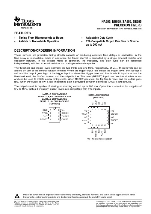
FEATURESDESCRIPTION/ORDERING INFORMATION12348765GNDTRIGOUTRESETVCCDISCHTHRESCONT3212019910111213456781817161514NCDISCHNCTHRESNCNCTRIGNCOUTNCNCGNDNCCONTNCVCCNCNCRESETNCNC – No internal connectionNA555...D OR P PACKAGENE555...D,P,PS,OR PW PACKAGESA555...D OR P PACKAGESE555...D,JG,OR P PACKAGE(TOP VIEW)SE555...FK PACKAGE(TOP VIEW)NA555,NE555,SA555,SE555PRECISION TIMERSSLFS022F–SEPTEMBER1973–REVISED JUNE2006•Timing From Microseconds to Hours•Adjustable Duty Cycle•Astable or Monostable Operation•TTL-Compatible Output Can Sink or Sourceup to200mAThese devices are precision timing circuits capable of producing accurate time delays or oscillation.In the time-delay or monostable mode of operation,the timed interval is controlled by a single external resistor and capacitor network.In the astable mode of operation,the frequency and duty cycle can be controlled independently with two external resistors and a single external capacitor.The threshold and trigger levels normally are two-thirds and one-third,respectively,of V CC.These levels can be altered by use of the control-voltage terminal.When the trigger input falls below the trigger level,the flip-flop is set,and the output goes high.If the trigger input is above the trigger level and the threshold input is above the threshold level,the flip-flop is reset and the output is low.The reset(RESET)input can override all other inputs and can be used to initiate a new timing cycle.When RESET goes low,the flip-flop is reset,and the output goes low.When the output is low,a low-impedance path is provided between discharge(DISCH)and ground.The output circuit is capable of sinking or sourcing current up to200mA.Operation is specified for supplies of 5V to15V.With a5-V supply,output levels are compatible with TTL inputs.Please be aware that an important notice concerning availability,standard warranty,and use in critical applications of TexasInstruments semiconductor products and disclaimers thereto appears at the end of this data sheet.PRODUCTION DATA information is current as of publication date.Copyright©1973–2006,Texas Instruments Incorporated Products conform to specifications per the terms of the Texas On products compliant to MIL-PRF-38535,all parameters are Instruments standard warranty.Production processing does not tested unless otherwise noted.On all other products,production necessarily include testing of all parameters.processing does not necessarily include testing of all parameters.NA555,NE555,SA555,SE555PRECISION TIMERSSLFS022F–SEPTEMBER 1973–REVISED JUNE 2006ORDERING INFORMATIONV THRES T AMAX PACKAGE (1)ORDERABLE PART NUMBER TOP-SIDE MARKING V CC =15VPDIP –P Tube of 50NE555P NE555P Tube of 75NE555D SOIC –DNE555Reel of 2500NE555DR 0°C to 70°C11.2VSOP –PS Reel of 2000NE555PSR N555Tube of 150NE555PW TSSOP –PW N555Reel of 2000NE555PWR PDIP –PTube of 50SA555P SA555P –40°C to 85°C11.2VTube of 75SA555D SOIC –D SA555Reel of 2000SA555DR PDIP –PTube of 50NA555P NA555P –40°C to 105°C11.2VTube of 75NA555D SOIC –D NA555Reel of 2000NA555DR PDIP –PTube of 50SE555P SE555P Tube of 75SE555D SOIC –D SE555D –55°C to 125°C10.6Reel of 2500SE555DR CDIP –JG Tube of 50SE555JG SE555JG LCCC –FKTube of 55SE555FKSE555FK(1)Package drawings,standard packing quantities,thermal data,symbolization,and PCB design guidelines are available at /sc/package.FUNCTION TABLETRIGGER THRESHOLD DISCHARGE RESET OUTPUT VOLTAGE (1)VOLTAGE (1)SWITCHLow Irrelevant Irrelevant Low On High <1/3V DD Irrelevant High Off High >1/3V DD >2/3V DD LowOnHigh>1/3V DD<2/3V DDAs previously established(1)Voltage levels shown are nominal.2Submit Documentation FeedbackTRIGTHRESOUTDISCHPin numbers shown are for the D, JG, P , PS, and PW packages.NOTE A:RESET can override TRIG, which can override THRES.NA555,NE555,SA555,SE555PRECISION TIMERSSLFS022F–SEPTEMBER 1973–REVISED JUNE 2006FUNCTIONAL BLOCK DIAGRAM3Submit Documentation FeedbackAbsolute Maximum Ratings (1)Recommended Operating ConditionsNA555,NE555,SA555,SE555PRECISION TIMERSSLFS022F–SEPTEMBER 1973–REVISED JUNE 2006over operating free-air temperature range (unless otherwise noted)MINMAX UNIT V CC Supply voltage (2)18V V I Input voltage CONT,RESET,THRES,TRIGV CC V I OOutput current±225mAD package97P package 85θJAPackage thermal impedance (3)(4)°C/W PS package 95PW package149FK package 5.61θJC Package thermal impedance (5)(6)°C/W JG package14.5T JOperating virtual junction temperature 150°C Case temperature for 60sFK package 260°C Lead temperature 1,6mm (1/16in)from case for 60sJG package300°C T stg Storage temperature range–65150°C (1)Stresses beyond those listed under "absolute maximum ratings"may cause permanent damage to the device.These are stress ratings only,and functional operation of the device at these or any other conditions beyond those indicated under "recommended operating conditions"is not implied.Exposure to absolute-maximum-rated conditions for extended periods may affect device reliability.(2)All voltage values are with respect to GND.(3)Maximum power dissipation is a function of T J (max),θJA ,and T A .The maximum allowable power dissipation at any allowable ambient temperature is P D =(T J (max)-T A )/θJA.Operating at the absolute maximum T J of 150°C can affect reliability.(4)The package thermal impedance is calculated in accordance with JESD 51-7.(5)Maximum power dissipation is a function of T J (max),θJC ,and T C .The maximum allowable power dissipation at any allowable case temperature is P D =(T J (max)-T C )/θJC .Operating at the absolute maximum T J of 150°C can affect reliability.(6)The package thermal impedance is calculated in accordance with MIL-STD-883.over operating free-air temperature range (unless otherwise noted)MINMAX UNIT NA555,NE555,SA555 4.516V CC Supply voltage V SE5554.518V I Input voltage CONT,RESET,THRES,and TRIGV CC V I OOutput current±200mANA555–40105NE555070T AOperating free-air temperature°C SA555–4085SE555–551254Submit Documentation FeedbackElectrical CharacteristicsNA555,NE555,SA555,SE555PRECISION TIMERS SLFS022F–SEPTEMBER1973–REVISED JUNE2006V CC =5V to15V,TA=25°C(unless otherwise noted)NA555SE555NE555PARAMETER TEST CONDITIONS UNITSA555MIN TYP MAX MIN TYP MAX V CC=15V9.41010.68.81011.2THRES voltage level V V CC=5V 2.7 3.34 2.4 3.3 4.2THRES current(1)3025030250nA4.855.2 4.55 5.6V CC=15VT A=–55°C to125°C36TRIG voltage level V1.45 1.67 1.9 1.1 1.672.2V CC=5VT A=–55°C to125°C 1.9TRIG current TRIG at0V0.50.90.52µA0.30.710.30.71RESET voltage level V T A=–55°C to125°C 1.1RESET at V CC0.10.40.10.4RESET current mA RESET at0V–0.4–1–0.4–1.5DISCH switch off-state2010020100nA current9.61010.491011V CC=15VT A=–55°C to125°C9.610.4CONT voltageV (open circuit) 2.9 3.3 3.8 2.6 3.34V CC=5VT A=–55°C to125°C 2.9 3.80.10.150.10.25V CC=15V,I OL=10mAT A=–55°C to125°C0.20.40.50.40.75V CC=15V,I OL=50mAT A=–55°C to125°C12 2.22 2.5V CC=15V,I OL=100mALow-level output voltage T A=–55°C to125°C 2.7VV CC=15V,I OL=200mA 2.5 2.5V CC=5V,I OL=3.5mA T A=–55°C to125°C0.350.10.20.10.35V CC=5V,I OL=5mAT A=–55°C to125°C0.8V CC=5V,I OL=8mA0.150.250.150.41313.312.7513.3V CC=15V,I OL=–100mAT A=–55°C to125°C12High-level output voltage V CC=15V,I OH=–200mA12.512.5V3 3.3 2.75 3.3V CC=15V,I OL=–100mAT A=–55°C to125°C2V CC=15V10121015Output low,No loadV CC=5V3536Supply current mAV CC=15V910913Output high,No loadV CC=5V2425(1)This parameter influences the maximum value of the timing resistors R A and R B in the circuit of Figure12.For example,when V CC=5V,the maximum value is R=R A+R B≈3.4MΩ,and for V CC=15V,the maximum value is10MΩ.5Submit Documentation FeedbackOperating CharacteristicsNA555,NE555,SA555,SE555PRECISION TIMERSSLFS022F–SEPTEMBER 1973–REVISED JUNE 2006V CC =5V to 15V,T A =25°C (unless otherwise noted)NA555SE555NE555TESTPARAMETERUNITSA555CONDITIONS (1)MINTYP MAX MINTYP MAXEach timer,monostable (3)T A =25°C0.5 1.5(4)13Initial error of timing %interval (2)Each timer,astable (5) 1.5 2.25Each timer,monostable (3)T A =MIN to MAX 30100(4)50Temperature coefficient of ppm/timing interval°C Each timer,astable (5)90150Each timer,monostable (3)T A =25°C 0.050.2(4)0.10.5Supply-voltage sensitivity of %/V timing interval Each timer,astable (5)0.150.3C L =15pF,Output-pulse rise time 100200(4)100300ns T A =25°C C L =15pF,Output-pulse fall time 100200(4)100300ns T A =25°C (1)For conditions shown as MIN or MAX,use the appropriate value specified under recommended operating conditions.(2)Timing interval error is defined as the difference between the measured value and the average value of a random sample from each process run.(3)Values specified are for a device in a monostable circuit similar to Figure 9,with the following component values:R A =2k Ωto 100k Ω,C =0.1µF.(4)On products compliant to MIL-PRF-38535,this parameter is not production tested.(5)Values specified are for a device in an astable circuit similar to Figure 12,with the following component values:R A =1k Ωto 100k Ω,C =0.1µF.6Submit Documentation FeedbackTYPICAL CHARACTERISTICSI OL − Low-Level Output Current − mALOW-LEVEL OUTPUT VOLTAGEvsLOW-LEVEL OUTPUT CURRENT− L o w -L e v e l O u t p u t V o l t a g e − VV O LLOW-LEVEL OUTPUT VOLTAGEvsLOW-LEVEL OUTPUT CURRENT− L o w -L e v e l O u t p u t V o l t a g e − VV O L I OL − Low-Level Output Current − mA0.020.22LOW-LEVEL OUTPUT VOLTAGEvsLOW-LEVEL OUTPUT CURRENT− L o w -L e v e l O u t p u t V o l t a g e− VV O L I OL − Low-Level Output Current − mA 10.60.201.41.82.00.41.60.81.2− I OH − High-Level Output Current − mAV C C V O H − V o l t a g e D r o p − V)(DROP BETWEEN SUPPLY VOLTAGE AND OUTPUTvsHIGH-LEVEL OUTPUT CURRENTNA555,NE555,SA555,SE555PRECISION TIMERSSLFS022F–SEPTEMBER 1973–REVISED JUNE 2006Data for temperatures below 0°C and above 70°C are applicable for SE555circuits only.Figure 1.Figure 2.Figure 3.Figure 4.7Submit Documentation Feedback567891011− S u p p l y C u r r e n t − m ASUPPLY CURRENTvsSUPPLY VOLTAGE12131415C C I V CC − Supply Voltage − V10.9950.9900.9855101.0051.010NORMALIZED OUTPUT PULSE DURATION(MONOSTABLE OPERATION)vsSUPPLY VOLTAGE1.0151520C CV P u l s e D u r a t i o nR e l a t i v e t o V a l u e a t = 10 V V CC − Supply Voltage − V−75−2525NORMALIZED OUTPUT PULSE DURATION(MONOSTABLE OPERATION)vsFREE-AIR TEMPERATURE75125T A − Free-Air Temperature − °C−5050100P u l s e D u r a t i o n R e l a t i v e t o V a l u e a t T A = 255C− P r o p a g a t i o n D e l a y T i m e − n sPROPAGATION DELAY TIMEvsLOWEST VOLTAGE LEVEL OF TRIGGER PULSELowest Voltage Level of Trigger Pulset P D 00.1 x V CC0.2 x V CC0.3 x V CC0.4 x V CCNA555,NE555,SA555,SE555PRECISION TIMERSSLFS022F–SEPTEMBER 1973–REVISED JUNE 2006TYPICAL CHARACTERISTICS (continued)Data for temperatures below 0°C and above 70°C are applicable for SE555circuits only.Figure 5.Figure 6.Figure 7.Figure 8.8Submit Documentation FeedbackAPPLICATION INFORMATIONMonostable OperationV CC(5 V to 15 V)OutputInputPin numbers shown are for the D, JG, P , PS, and PW packages.NA555,NE555,SA555,SE555PRECISION TIMERSSLFS022F–SEPTEMBER 1973–REVISED JUNE 2006For monostable operation,any of these timers can be connected as shown in Figure 9.If the output is low,application of a negative-going pulse to the trigger (TRIG)sets the flip-flop (Q goes low),drives the output high,and turns off Q1.Capacitor C then is charged through R A until the voltage across the capacitor reaches the threshold voltage of the threshold (THRES)input.If TRIG has returned to a high level,the output of the threshold comparator resets the flip-flop (Q goes high),drives the output low,and discharges C through Q1.Figure 9.Circuit for Monostable OperationMonostable operation is initiated when TRIG voltage falls below the trigger threshold.Once initiated,the sequence ends only if TRIG is high at the end of the timing interval.Because of the threshold level and saturation voltage of Q1,the output pulse duration is approximately t w =1.1R A C.Figure 11is a plot of the time constant for various values of R A and C.The threshold levels and charge rates both are directly proportional to the supply voltage,V CC .The timing interval is,therefore,independent of the supply voltage,so long as the supply voltage is constant during the time interval.Applying a negative-going trigger pulse simultaneously to RESET and TRIG during the timing interval discharges C and reinitiates the cycle,commencing on the positive edge of the reset pulse.The output is held low as long as the reset pulse is low.To prevent false triggering,when RESET is not used,it should be connected to V CC .9Submit Documentation Feedback− O u t p u t P u l s e D u r a t i o n − sC − Capacitance − µF10110−110−210−310−410−5t w V o l t a g e − 2 V /d i vTime − 0.1 ms/divAstable OperationV o l t a g e − 1 V /d i vTime − 0.5 ms/divttR R OutputL V CCNOTE A:Decoupling CONT voltage to ground with a capacitor canimprove operation. This should be evaluated for individual applications.Pin numbers shown are for the D, JG, P , PS, and PW packages.NA555,NE555,SA555,SE555PRECISION TIMERSSLFS022F–SEPTEMBER 1973–REVISED JUNE 2006APPLICATION INFORMATION (continued)Figure 10.Typical Monostable Waveforms Figure 11.Output Pulse Duration vs CapacitanceAs shown in Figure 12,adding a second resistor,R B ,to the circuit of Figure 9and connecting the trigger input to the threshold input causes the timer to self-trigger and run as a multivibrator.The capacitor C charges through R A and R B and then discharges through R B only.Therefore,the duty cycle is controlled by the values of R A and R B .This astable connection results in capacitor C charging and discharging between the threshold-voltage level (≈0.67×V CC )and the trigger-voltage level (≈0.33×V CC ).As in the monostable circuit,charge and discharge times (and,therefore,the frequency and duty cycle)are independent of the supply voltage.Figure 12.Circuit for Astable Operation Figure 13.Typical Astable Waveforms10Submit Documentation FeedbacktH+0.693(R A )R B)Ct L +0.693(R B)C Other useful relationships are shown below.period +t H )t L +0.693(R A )2R B)Cfrequency [1.44(R A )2R B )C Output driver duty cycle +tL t H )t L +RB R A )2R B Output waveform duty cycle+t L t H +R B R A )R BLow-to-high ratio +t H t H )t L +1–R B R A )2R Bf − F r e e -R u n n i ng F r e q u e n c y − H zC − Capacitance − µF1001010.10.010.001Missing-PulseDetectorTime − 0.1 ms/divV o l t a g e − 2 V /d i vPin numbers shown are shown for the D, JG, P , PS, and PW packages.NA555,NE555,SA555,SE555PRECISION TIMERSSLFS022F–SEPTEMBER 1973–REVISED JUNE 2006APPLICATION INFORMATION (continued)Figure 13shows typical waveforms generated during astable operation.The output high-level duration t H and low-level duration t L can be calculated as follows:Figure 14.Free-Running FrequencyThe circuit shown in Figure 15can be used to detect a missing pulse or abnormally long spacing between consecutive pulses in a train of pulses.The timing interval of the monostable circuit is retriggered continuously by the input pulse train as long as the pulse spacing is less than the timing interval.A longer pulse spacing,missing pulse,or terminated pulse train permits the timing interval to be completed,thereby generating an output pulse as shown in Figure 16.Figure 15.Circuit for Missing-Pulse DetectorFigure pleted Timing Waveforms forMissing-Pulse DetectorFrequency DividerV o l t a g e − 2 V /d i vTime − 0.1 ms/divNA555,NE555,SA555,SE555PRECISION TIMERSSLFS022F–SEPTEMBER 1973–REVISED JUNE 2006APPLICATION INFORMATION (continued)By adjusting the length of the timing cycle,the basic circuit of Figure 9can be made to operate as a frequency divider.Figure 17shows a divide-by-three circuit that makes use of the fact that retriggering cannot occur during the timing cycle.Figure 17.Divide-by-Three Circuit WaveformsPulse-Width ModulationCAV (5 V to 15 V)OutputModulationInput(see Note A)Clock InputNOTE A:The modulating signal can be direct or capacitively coupledto CONT . For direct coupling, the effects of modulation source voltage and impedance on the bias of the timer should be considered.Pin numbers shown are for the D, JG, P , PS, and PW packages.V o l t a g e − 2 V /d i vTime − 0.5 ms/divNA555,NE555,SA555,SE555PRECISION TIMERSSLFS022F–SEPTEMBER 1973–REVISED JUNE 2006APPLICATION INFORMATION (continued)The operation of the timer can be modified by modulating the internal threshold and trigger voltages,which is accomplished by applying an external voltage (or current)to CONT.Figure 18shows a circuit for pulse-width modulation.A continuous input pulse train triggers the monostable circuit,and a control signal modulates the threshold voltage.Figure 19shows the resulting output pulse-width modulation.While a sine-wave modulation signal is shown,any wave shape could be used.Figure 18.Circuit for Pulse-Width Modulation Figure 19.Pulse-Width-Modulation WaveformsPulse-Position ModulationV o l t a g e − 2 V /d i vTime − 0.1 ms/divNOTE A:The modulating signal can be direct or capacitively coupledto CONT . For direct coupling, the effects of modulation source voltage and impedance on the bias of the timer should be considered.Pin numbers shown are for the D, JG, P , PS, and PW packages.OutputNA555,NE555,SA555,SE555PRECISION TIMERSSLFS022F–SEPTEMBER 1973–REVISED JUNE 2006APPLICATION INFORMATION (continued)As shown in Figure 20,any of these timers can be used as a pulse-position modulator.This application modulates the threshold voltage and,thereby,the time delay,of a free-running oscillator.Figure 21shows a triangular-wave modulation signal for such a circuit;however,any wave shape could be used.Figure 20.Circuit for Pulse-Position Modulation Figure 21.Pulse-Position-Modulation WaveformsSequential TimerC B = 4.7 µF R B = 100 k ΩPin numbers shown are for the D, JG, P , PS, and PW packages.NOTE A:S closes momentarily at t = 0.V o l t a g e − 5 V /d i vt − Time − 1 s/divNA555,NE555,SA555,SE555PRECISION TIMERSSLFS022F–SEPTEMBER 1973–REVISED JUNE 2006APPLICATION INFORMATION (continued)Many applications,such as computers,require signals for initializing conditions during start-up.Other applications,such as test equipment,require activation of test signals in sequence.These timing circuits can be connected to provide such sequential control.The timers can be used in various combinations of astable or monostable circuit connections,with or without modulation,for extremely flexible waveform control.Figure 22shows a sequencer circuit with possible applications in many systems,and Figure 23shows the output waveforms.Figure 22.Sequential Timer CircuitFigure 23.Sequential Timer WaveformsPACKAGING INFORMATIONOrderableDevice Status (1)Package Type Package Drawing Pins Package Qty Eco Plan (2)Lead/Ball Finish MSL Peak Temp (3)JM38510/10901BPAACTIVE CDIP JG 81TBD A42SNPB N /A for Pkg Type NA555D ACTIVE SOIC D 875Green (RoHS &no Sb/Br)CU NIPDAU Level-1-260C-UNLIM NA555DG4ACTIVE SOIC D 875Green (RoHS &no Sb/Br)CU NIPDAU Level-1-260C-UNLIM NA555DR ACTIVE SOIC D 82500Green (RoHS &no Sb/Br)CU NIPDAU Level-1-260C-UNLIM NA555DRG4ACTIVE SOIC D 82500Green (RoHS &no Sb/Br)CU NIPDAU Level-1-260C-UNLIM NA555P ACTIVE PDIP P 850Pb-Free (RoHS)CU NIPDAU N /A for Pkg Type NA555PE4ACTIVE PDIP P 850Pb-Free (RoHS)CU NIPDAU N /A for Pkg Type NE555D ACTIVE SOIC D 875Green (RoHS &no Sb/Br)CU NIPDAU Level-1-260C-UNLIM NE555DE4ACTIVE SOIC D 875Green (RoHS &no Sb/Br)CU NIPDAU Level-1-260C-UNLIM NE555DG4ACTIVE SOIC D 875Green (RoHS &no Sb/Br)CU NIPDAU Level-1-260C-UNLIM NE555DR ACTIVE SOIC D 82500Green (RoHS &no Sb/Br)CU NIPDAU Level-1-260C-UNLIM NE555DRE4ACTIVE SOIC D 82500Green (RoHS &no Sb/Br)CU NIPDAU Level-1-260C-UNLIM NE555DRG4ACTIVE SOIC D 82500Green (RoHS &no Sb/Br)CU NIPDAU Level-1-260C-UNLIM NE555P ACTIVE PDIP P 850Pb-Free (RoHS)CU NIPDAU N /A for Pkg Type NE555PE4ACTIVE PDIP P 850Pb-Free (RoHS)CU NIPDAU N /A for Pkg Type NE555PSLE OBSOLETE SO PS 8TBDCall TI Call TINE555PSR ACTIVE SO PS 82000Green (RoHS &no Sb/Br)CU NIPDAU Level-1-260C-UNLIM NE555PSRE4ACTIVE SO PS 82000Green (RoHS &no Sb/Br)CU NIPDAU Level-1-260C-UNLIM NE555PW ACTIVE TSSOP PW 8150Green (RoHS &no Sb/Br)CU NIPDAU Level-1-260C-UNLIM NE555PWE4ACTIVE TSSOP PW 8150Green (RoHS &no Sb/Br)CU NIPDAU Level-1-260C-UNLIM NE555PWR ACTIVE TSSOP PW 82000Green (RoHS &no Sb/Br)CU NIPDAU Level-1-260C-UNLIM NE555PWRE4ACTIVE TSSOPPW82000Green (RoHS &no Sb/Br)CU NIPDAU Level-1-260C-UNLIM NE555Y OBSOLETE 0TBD Call TI Call TISA555D ACTIVE SOIC D 875Green (RoHS &no Sb/Br)CU NIPDAU Level-1-260C-UNLIM SA555DE4ACTIVE SOIC D 875Green (RoHS &no Sb/Br)CU NIPDAU Level-1-260C-UNLIM SA555DG4ACTIVESOICD875Green (RoHS &no Sb/Br)CU NIPDAULevel-1-260C-UNLIM31-Jul-2006Orderable DeviceStatus (1)Package Type Package DrawingPins Package Qty Eco Plan (2)Lead/Ball Finish MSL Peak Temp (3)SA555DR ACTIVE SOIC D 82500Green (RoHS &no Sb/Br)CU NIPDAU Level-1-260C-UNLIM SA555DRE4ACTIVE SOIC D 82500Green (RoHS &no Sb/Br)CU NIPDAU Level-1-260C-UNLIM SA555DRG4ACTIVE SOIC D 82500Green (RoHS &no Sb/Br)CU NIPDAU Level-1-260C-UNLIM SA555P ACTIVE PDIP P 850Pb-Free (RoHS)CU NIPDAU N /A for Pkg Type SA555PE4ACTIVE PDIP P 850Pb-Free (RoHS)CU NIPDAU N /A for Pkg Type SE555D ACTIVE SOIC D 875TBD CU NIPDAU Level-1-220C-UNLIM SE555DR ACTIVE SOIC D 82500TBD CU NIPDAU Level-1-220C-UNLIM SE555FKB ACTIVE LCCC FK 201TBD POST-PLATE N /A for Pkg TypeSE555JG ACTIVE CDIP JG 81TBD A42SNPB N /A for Pkg Type SE555JGB ACTIVE CDIP JG 81TBD A42SNPB N /A for Pkg Type SE555N OBSOLETE PDIP N 8TBD Call TI Call TISE555PACTIVEPDIPP850Pb-Free (RoHS)CU NIPDAUN /A for Pkg Type(1)The marketing status values are defined as follows:ACTIVE:Product device recommended for new designs.LIFEBUY:TI has announced that the device will be discontinued,and a lifetime-buy period is in effect.NRND:Not recommended for new designs.Device is in production to support existing customers,but TI does not recommend using this part in a new design.PREVIEW:Device has been announced but is not in production.Samples may or may not be available.OBSOLETE:TI has discontinued the production of the device.(2)Eco Plan -The planned eco-friendly classification:Pb-Free (RoHS),Pb-Free (RoHS Exempt),or Green (RoHS &no Sb/Br)-please check /productcontent for the latest availability information and additional product content details.TBD:The Pb-Free/Green conversion plan has not been defined.Pb-Free (RoHS):TI's terms "Lead-Free"or "Pb-Free"mean semiconductor products that are compatible with the current RoHS requirements for all 6substances,including the requirement that lead not exceed 0.1%by weight in homogeneous materials.Where designed to be soldered at high temperatures,TI Pb-Free products are suitable for use in specified lead-free processes.Pb-Free (RoHS Exempt):This component has a RoHS exemption for either 1)lead-based flip-chip solder bumps used between the die and package,or 2)lead-based die adhesive used between the die and leadframe.The component is otherwise considered Pb-Free (RoHS compatible)as defined above.Green (RoHS &no Sb/Br):TI defines "Green"to mean Pb-Free (RoHS compatible),and free of Bromine (Br)and Antimony (Sb)based flame retardants (Br or Sb do not exceed 0.1%by weight in homogeneous material)(3)MSL,Peak Temp.--The Moisture Sensitivity Level rating according to the JEDEC industry standard classifications,and peak solder temperature.Important Information and Disclaimer:The information provided on this page represents TI's knowledge and belief as of the date that it is provided.TI bases its knowledge and belief on information provided by third parties,and makes no representation or warranty as to the accuracy of such information.Efforts are underway to better integrate information from third parties.TI has taken and continues to take reasonable steps to provide representative and accurate information but may not have conducted destructive testing or chemical analysis on incoming materials and chemicals.TI and TI suppliers consider certain information to be proprietary,and thus CAS numbers and other limited information may not be available for release.In no event shall TI's liability arising out of such information exceed the total purchase price of the TI part(s)at issue in this document sold by TI to Customer on an annual basis.31-Jul-2006IMPORTANT NOTICETexas Instruments Incorporated and its subsidiaries (TI) reserve the right to make corrections, modifications, enhancements, improvements, and other changes to its products and services at any time and to discontinue any product or service without notice. Customers should obtain the latest relevant information before placing orders and should verify that such information is current and complete. All products are sold subject to TI’s terms and conditions of sale supplied at the time of order acknowledgment.TI warrants performance of its hardware products to the specifications applicable at the time of sale in accordance with TI’s standard warranty. T esting and other quality control techniques are used to the extent TI deems necessary to support this warranty. Except where mandated by government requirements, testing of all parameters of each product is not necessarily performed.TI assumes no liability for applications assistance or customer product design. Customers are responsible for their products and applications using TI components. T o minimize the risks associated with customer products and applications, customers should provide adequate design and operating safeguards.TI does not warrant or represent that any license, either express or implied, is granted under any TI patent right, copyright, mask work right, or other TI intellectual property right relating to any combination, machine, or process in which TI products or services are used. Information published by TI regarding third-party products or services does not constitute a license from TI to use such products or services or a warranty or endorsement thereof. Use of such information may require a license from a third party under the patents or other intellectual property of the third party, or a license from TI under the patents or other intellectual property of TI.Reproduction of information in TI data books or data sheets is permissible only if reproduction is without alteration and is accompanied by all associated warranties, conditions, limitations, and notices. Reproduction of this information with alteration is an unfair and deceptive business practice. TI is not responsible or liable for such altered documentation.Resale of TI products or services with statements different from or beyond the parameters stated by TI for that product or service voids all express and any implied warranties for the associated TI product or service and is an unfair and deceptive business practice. TI is not responsible or liable for any such statements. Following are URLs where you can obtain information on other Texas Instruments products and application solutions:Products ApplicationsAmplifiers Audio /audioData Converters Automotive /automotiveDSP Broadband /broadbandInterface Digital Control /digitalcontrolLogic Military /militaryPower Mgmt Optical Networking /opticalnetwork Microcontrollers Security /securityLow Power Wireless /lpw Telephony /telephonyVideo & Imaging /videoWireless /wirelessMailing Address:Texas InstrumentsPost Office Box 655303 Dallas, Texas 75265Copyright 2006, Texas Instruments Incorporated。
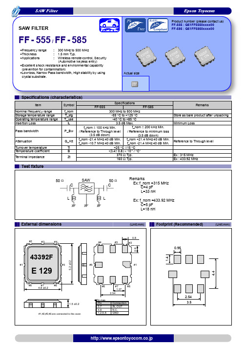
FF-555资料
broadband and ubiquitous society, we are committed to offering products
that are one step ahead of the market and a rank above the rest in quality.
To achieve our goals, we follow a “3D (three device) strategy” designed to
f_nom -10.7 MHz 40 dB Min. f_nom -21.4 MHz 40 dB Min.
+25 °C ±15 °C -(3.4± 0.8) × 10-8 / °C2
370 Ω Typ.
160 Ω Typ.
Remarks Store as bare product after unpacking Minimum Loss
f_nom ± 200 kHz Min.
/ Reference to Through level / Reference to minimum loss
(3.5 dB down)
(3.5 dB down)
f_nom -21.4 MHz 40 dB Min. f_nom +21.4 MHz 40 dB Min.
(Automotive keyless entry)
•Excellent shock resistance and environmental capability
完整版NE555中文资料

NE555中文资料通用时基电路NE555P概述:封装外形图NE555P是一块通用时基电路,电路包含24个晶体管,2 个二极管和17个电阻,组成阈值比较器,触发比较器,RS 触发器,复位输入,放电和输出等6部分。
采用DIP8、S0P8封装形式。
主要特点:关闭时间小于2 S o最大工作频率大于500kHz。
定时可从微秒级至小时级(由外接电阻电容精确控制)可工作于振荡方式或单稳态方式。
输出电流大,200mA (可提供或灌入)。
占空比可调。
可同TTL电路相接。
温度稳定性好,0.005%/C功能框图极限值(绝对最大额定值,若无其它规定,Tamb=25C)(若无其它规定,Vcc=5~15V , Tamb=25应用图555芯片引脚图及引脚描述555的8脚是集成电路工作电压输入端,电压为5〜18V ,以UCC 表示;从分压器上看出,上比较器6脚A1的5脚接在 R1和R2之间,所以5脚的电压固定在 2UCC/3上;下比 较器A2接在R2与R3之间,A2的同相输入端电位被固定在 UCC/3上。
NE555管脚功能介绍:1脚为地。
2脚为触发输入端;3脚为输出端,输出的电平状态受触发器控制,而触发 器受上比较器6脚和下比较器2脚的控制。
当触发器接受上比较器 A1从R 脚输入的高电平时,触发器被置于复位状态, 3脚输出低电平;2脚和6脚是互补的,2脚只对低电平起作用,高电平对它不起作用,即电压小于1UCC/3 , 此时3脚输出高电平。
6脚为阈值端,只对高电平起作用,低电平对它不起作用,即输入 电 压大于2 Ucc/3,称高触发端,3脚输出低电平,但有一个先决条件,即 2脚电位必须大于1.单稳态延时电路V ;TVo -)丄工3.开机延迟电路:接通电源输岀Vo 由低跳变到高而延迟的电路。
延迟时间:td=1.1RCVo丄HFUAU o0. 01 uF 1 01WIH-O Vc c启动4.开机延迟电路:接通电源输岀 由高跳变到低而延迟的电路。
555电路原理

555电路原理
555电路原理是一种常用的集成电路,其主要功能是产生稳定
的时序信号。
555电路原理的核心是一对比较器、一个RS触
发器和一对输出驱动器。
比较器是555电路原理的核心部分,其作用是根据输入信号的电平大小来判断输出信号的高低电平。
RS触发器是一个状态
存储器,通常由两个互补的触发器构成。
当RS触发器的S端(Set)和R端(Reset)分别接收到高电平信号时,触发器的
输出状态会相应变化。
输出驱动器则用来驱动外部负载,使得555电路原理的输出信号能够对外部设备产生影响。
555电路原理的工作原理是基于固定的参考电压和可调的阈值
电压来产生稳定的时序信号。
当输入电压超过阈值电压时,输出会由低电平变为高电平;当输入电压低于阈值电压时,输出会由高电平变为低电平。
而输入电压和阈值电压之间的差值决定了输出信号的时间周期。
555电路原理在实际应用中具有广泛的用途,例如用作定时器、频率计、脉冲发生器等。
它的简单可靠和灵活性使得它成为电子工程师常用的集成电路之一。
NE555中文资料
图一
图二
图三 表 1 是 NE555 的极限参数,不同的封装形式及不同的生产厂商的器件这些参数不尽相同,极限参数是指在不损坏器件的情况下,厂商保 证的界限,并非可以工作的条件,如果超过某一环境下使用,其间的安全性将不会得到保证,这使用中应加以注意。
NE555 的极限参数 电源电压 允许功耗
NE555 时基电路封装形式有两种,一是 DIP 双列直插 8 脚封装,另一种是 SOP-8 小型(SMD)封装形式。其他 HA17555、LM555、CA555 分属不同的公 司生产的产品。内部结构和工作原理都相同。NE555 属于 CMOS 工艺制造,下面我们将对其进行介绍。
图 1 是 NE555 的外形图,图 2 是它的内部功能原理框图,图 3 是它的内部等效电路。NE555 的内部中心电路是三极管 Q15 和 Q17 加正反馈 组成的 RS 触发器。输入控制端有直接复位 Reset 端,通过比较器 A1,复位控制端的 TH、比较器 A2 置位控制的 T。输出端为 F,另外还有集电极开 路的放电管 DIS。它们控制的优先权是 R、T、TH。
参数功能特性: •供应电压 4.5-18V •供应电流 3-6 mA •输出电流 225mA (max) •上升/下降时间 100 ns .NE555 的相关应用: NE555 的作用范围很广,但一般多应用于单稳态多谐振荡器(Monostable Mutlivibrator)及无稳态多谐振荡器(Astable Multivibrator)。 NE555 在线计算器 555 集成电路参数应用计算
NE555 是属于 555 系列的计时 IC 的其中的一种型号,555 系列 IC 的接脚功能及运用都是相容的,只是型号不同的因其价格不同其稳定度、省电、 可产生的振荡频率也不大相同;而 555 是一个用途很广且相当普遍的计时 IC,只需少数的电阻和电容,便可产生数位电路所需的各种不同频率之脉 冲信号。
555使用手册
555使用手册(原创实用版)目录1.555 使用手册概述2.555 的安装与设置3.555 的功能与特点4.555 的使用方法与技巧5.555 的维护与升级6.555 的常见问题与解答正文【555 使用手册概述】555 是一款高效实用的工具软件,为广大用户提供了方便快捷的服务。
本手册将为您详细介绍如何安装、设置和使用 555,让您充分发挥其功能,提高工作效率。
【555 的安装与设置】555 的安装非常简单,只需根据提示进行操作即可。
安装完成后,打开软件,按照提示进行设置,包括基本信息、功能选项等。
设置完成后,即可开始使用 555。
【555 的功能与特点】555 具有以下功能与特点:1.多功能一体,集成了各种实用工具;2.操作简单易懂,即使是初学者也能快速上手;3.强大的数据处理能力,可以满足各种需求;4.支持多种文件格式,兼容性较强;5.支持云端存储,方便数据备份和共享。
【555 的使用方法与技巧】555 的使用方法如下:1.打开 555 软件,选择需要的功能模块;2.根据提示,导入或创建数据文件;3.利用软件提供的工具,对数据进行处理;4.处理完成后,保存或导出结果。
使用 555 时,可以掌握以下技巧:1.批量处理数据,提高效率;2.利用快捷键操作,节省时间;3.定期更新软件,获取新功能。
【555 的维护与升级】为了确保 555 的正常运行,需要定期进行维护。
具体操作如下:1.检查软件是否有异常,如有异常及时处理;2.定期更新软件版本,以获取新功能和修复漏洞;3.备份数据,防止数据丢失。
【555 的常见问题与解答】在使用 555 过程中,可能会遇到一些问题。
下面列举了一些常见问题及解答:1.问:question1(对应答案 1)2.问题 2(对应答案 2)3.问题 3(对应答案 3)通过本手册的介绍,相信您已经对 555 有了充分的了解,可以熟练地使用它来提高工作效率。
555电路及原理
555电路及原理
555电路及原理介绍:
555电路是一种非常常用的集成电路,广泛应用于定时器、频
率分频器、脉宽调制电路等各种电子设备中。
它的原理基于内部比较器和外部电阻电容网络的结合。
555电路内部包含三个主要功能模块:比较器、RS触发器和
放大器。
其中比较器负责将输入的电压与内部的基准电压进行比较,并产生相应的高电平或低电平输出。
RS触发器则用于
分配输入信号,根据不同的输入进行状态转换。
放大器则用于放大输出信号,并驱动外部电路。
555电路主要的引脚包括:电源引脚VCC和GND,控制引脚TRIGGER、THRESOLD和RESET,以及输出引脚OUT和DISCHARGE。
通过对不同引脚的控制,可以实现不同的功能。
比如,通过设置TRIGGER和THRESOLD的电压分压比,可
以产生不同的输出频率;通过连接外部电阻和电容,可以实现定时器的功能。
除了基本功能外,555电路还有很多扩展应用,比如脉宽调制(PWM)、方波发生器、斜波发生器等。
这些应用利用了555
电路的稳定性和可调性,使得其具有广泛的应用价值。
总结:555电路是一种常用的集成电路,利用内部的比较器和
外部的电阻电容网络,实现各种定时、频率和脉宽的控制。
通
过对不同引脚的控制和连接外部元件,可以实现丰富的电子功能。
555使用手册
555使用手册【原创实用版】目录1.555 使用手册概述2.555 的安装与设置3.555 的功能与应用4.555 的维护与升级5.555 的安全与注意事项正文【555 使用手册概述】555 使用手册是为了帮助用户更好地理解和使用 555 产品而编写的。
本文将详细介绍 555 的安装与设置、功能与应用、维护与升级、安全与注意事项等方面的内容,以帮助用户充分发挥 555 产品的优势,提高工作效率。
【555 的安装与设置】在开始使用 555 之前,请确保您已经正确安装了 555 产品。
以下是安装与设置的详细步骤:1.确认产品型号和规格是否与您的设备相匹配。
2.根据产品说明书中的指导,连接 555 产品到您的设备上。
3.启动设备,按照屏幕提示进行相关设置。
【555 的功能与应用】555 产品具有强大的功能,适用于各种场景。
以下是一些主要功能及其应用示例:1.文字输入:555 可以快速、准确地识别用户的文字输入,为用户提供便捷的文字处理功能。
2.语音识别:555 支持实时语音识别,可以帮助用户进行语音转文字的记录和整理。
3.图像识别:555 具备图像识别功能,可以识别并提取图像中的文字信息。
【555 的维护与升级】为了保证 555 产品的性能和稳定性,需要定期进行维护和升级。
以下是一些建议:1.定期检查设备连接是否正常,如有问题及时处理。
2.确保设备软件更新至最新版本,以获得更好的性能和功能。
3.遇到问题时,及时联系售后服务人员进行处理。
【555 的安全与注意事项】在使用 555 产品时,请注意以下几点以确保设备安全和个人信息安全:1.确保设备存放在干燥、通风的地方,避免阳光直射和潮湿环境。
2.不要在设备上安装未经授权的软件,以防病毒和恶意程序侵入。
3.切勿将设备用于非法用途,遵守我国相关法律法规。
通过以上介绍,相信您已经对 555 产品有了更加全面的了解。
- 1、下载文档前请自行甄别文档内容的完整性,平台不提供额外的编辑、内容补充、找答案等附加服务。
- 2、"仅部分预览"的文档,不可在线预览部分如存在完整性等问题,可反馈申请退款(可完整预览的文档不适用该条件!)。
- 3、如文档侵犯您的权益,请联系客服反馈,我们会尽快为您处理(人工客服工作时间:9:00-18:30)。
555芯片引脚图及引脚描述
555的8脚是集成电路工作电压输入端,电压为5~18V,以UCC表示;从分压器上看出,上比较器6脚A1的5脚接在R1和R2之间,所以5脚的电压固定在2UCC/3上;下比较器A2接在R2与R3之间,A2的同相输入端电位被固定在UCC/3上。
1脚为地。
2脚为触发输入端;3脚为输出端,输出的电平状态受触发器控制,而触发器受上比较器6脚和下比较器2脚的控制。
当触发器接受上比较器A1从R脚输入的高电平时,触发器被置于复位状态,3脚输出低电平;
2脚和6脚是互补的,2脚只对低电平起作用,高电平对它不起作用,即电压小于1Ucc/3,此时3脚输出高电平。
6脚为阈值端,只对高电平起作用,低电平对它不起作用,即输入电压大于2 Ucc/3,称高触发端,3脚输出低电平,但有一个先决条件,即2脚电位必须大于1Ucc/3时才有效。
3脚在高电位接近电源电压Ucc,输出电流最大可打200mA。
4脚是复位端,当4脚电位小于0.4V时,不管2、6脚状态如何,输出端3脚都输出低电平。
5脚是控制端。
7脚称放电端,与3脚输出同步,输出电平一致,但7脚并不输出电流,所以3脚称为实高(或低)、7脚称为虚高。
1 555集成电路的框图及工作原理
555集成电路开始是作定时器应用的,所以叫做555定时器或555时基电路。
但后来经过开发,它除了作定时延时控制外,还可用于调光、调温、调压、调速等多种控制及计量检测。
此外,还可以组成脉冲振荡、单稳、双稳和脉冲调制电路,用于交流信号源、电源变换、频率变换、脉冲调制等。
由于它工作可靠、使用方便、价格低廉,目前被广泛用于各种电子产品中,555集成电路内部有几十个元器件,有分压器、比较器、基本R-S触发器、放电管以及缓冲器等,电路比较复杂,是模拟电路和数字电路的混合体,如图1所示。
555芯片管脚介绍
555集成电路是8脚封装,双列直插型,如图2(A)所示,按输入输出的排列可看成如图2(B)所示。
其中6脚称阈值端(TH),是上比较器的输入;2脚称触发端(TR),是下比较器的输入;3脚是输出端(V o),它有O和1两种状态,由输入端所加的电平决定;7脚是放电端(DIS),它是内部放电管的输出,有悬空和接地两种状态,也是由输入端的状态决定;4脚是复位端(MR),加上低电平时可使输出为低电平;5脚是控制电压端(Vc),可用它改变上下触
发电平值;8脚是电源端,1脚是地端。
图2 555集成电路封装图
我们也可以把555电路等效成一个带放电开关的R-S触发器,如图3(A)所示,这个特殊的触发器有两个输入端:阈值端(TH)可看成是置零端R,要求高电平,触发端(TR)可看成是置位端S,要求低电平,有一个输出端Vo,Vo可等效成触发器的Q端,放电端(DIS)可看成是由内部放电开关控制的一个接点,由触发器的Q端控制:Q=1时DIS端接地,Q=0时DIS端悬空。
另外还有复位端MR,控制电压端Vc,电源端VDD和
地端GND。
这个特殊的触发器有两个特点:
(1)两个输入端的触发电平要求一高一低,置零端R即阈值端(TH)要求高电平,而置位端s 即触发端(TR)则要求低电乎;
(2)两个输入端的触发电平使输出发生翻转的阈值电压值也不同,当V c端不接控制电压时,对TH(R)端来讲,>2/3VDD是高电平1,<2/3VDD是低电平0:而对TR(S)端来讲,>1/3VDD 是高电平1,<1/3VDD是低电平0。
如果在控制端(Vc)上控制电压Vc时,这时上触发电平就变成Vc值,下触发电平就变成1/2Vc值,可见改变控制端的控制电压值就可以改变上下触发电平值。
它的功能表见图3(B)所示。
图3 555电路等效R—S触发器
555集成电路有双极型和CMOS型两种。
CMOS型的优点是功耗低、电源电压低、输入阻抗高,但输出功率较小,输出驱动电流只有几毫安。
双极型的优点是输出功率大,驱动电流达200毫安,其他指标则不如CMOS型的。
4. 典型应用电路
555的应用电路很多,只要改变555集成电路的外部附加电路,就可以构成几百种应用电路,大体上可分为555单稳、555双稳及555无稳(即振荡器)三类。
5 555单稳电路
单稳电路有一个稳态和一个暂稳态,是利用电容的充放电形成暂稳态的,因此它的输入端都带有定时电阻和定时电容,常见的555单稳电路有两种:
1)人工启动型
将555电路的6、2脚并接起来接在RC定时电路上,在定时电容CT,两端接按钮开关SB,就成为人工启动型555单稳电路,如图4(a)所示,用等效触发器替代555,并略去与单稳工作无关的部分后见图4(b)所示,下面分析它的工作原理:
稳态:接上电源后,电容CT很快充电到VDD,从图4(b)看到,触发器输入R=1,S=1,从功能表看到输出Vo=0,这是它的稳态。
暂稳态:按下开关SB,CT上电荷很快放到零,相当于触发器输入R=0,S=0,输出立即翻转成Vo=l,暂稳态开始。
开关放开后,电源又向CT充电,经过时间TD后,CT上电压上升到>2/3VDD时,输出又翻转成V o=O,暂稳态结束。
TD就是单稳电路的定时时间或延时时间,它和定时电阻RT和定时电容CT的值有关:TD=1.1RTCT。
图4人工启动型555单稳电路
2)脉冲启动型
将555电路的6、7脚并接起来接在定时电容CT上,用2脚作输入就成为脉冲启动型单稳电路,如图5(a)所示,电路的2脚平时接高电平,当输入接低电平或输入负脉冲时才启动电路,用等效触发器替代555后见图5 6)所示,下面分析它的工作原理:稳态:接上电源后,R=1,S=1,输出Vo=0,DIS端接地,CT上的电压为0即R=0,输出仍保持Vo=0,这是它的稳态。
暂稳态:输入负脉冲后,输入S=0,输出立即翻转成Vo=1,DIS端开路,电源通过RT 向CT充电,暂稳态开始。
经过时间TD后,CT上电压上升到>2/3VDD时,输入又成为R=1,S=1,这时负脉冲已经消失,输出又翻转成V o=0,暂稳态结束。
这时内部放电开关接通,DIS端接地,CT上电荷很快放到零,为下一次定时控制作准备。
电路的定时时间TD=1.1RTCT。
这两种单稳电路常用作定时延时控制。
图5脉冲启动型单稳电路
6 555双稳电路
常见的555双稳电路有两种:
1)R-S触发器型双稳
将555电路的6、2脚作为两个控制输入端,7端不用,就成为一个R-S触发器。
注意两个输入端的触发电平和阈值电压不同,如图6(a)所示,有时可能只有一个控制端,这时另外一个控制端要设法接死,根据电路要求可以把R端接到电源端,如图6(b)所示,也可以把S接地,用R端作输入。
有两个输入端的双稳电路常用作电机调速、电源上下限告警等用途。
有一个输入端的双稳电路作为单端比较器用于各种检测电路。
图6 555构成R-S触发器
2)施密特触发器型双稳
将555电路的6、2脚并接起来接成只有一个输入端的触发器,如图7(a)所示,这个触发器输出电压和输入电压的关系是一个长方形的回线形,如图7(b)所示,从曲线可知,当输入V1=0时输出V o=1,当输入电压从0上升到>2/3VDD后,Vo翻转成0,当输入电压从最高值下降到<1/3VDD后,V o又翻转成1。
由于它的输入有两个不同的阈值电压,所以,这种电路常用于电子开关,各种控制电路、波形的变换和整形,如图8所示。
图7 555构成施密特触发器
图8波形的变换和整形
6. 555振荡器电路(无稳电路)
由555定时器构成的多谐振荡器如图9(a)所示,其工作波形见图9(b)。
接通电源后,电源VDD通过R1和R2对电容C充电,当Uc<1/3VDD时,振荡器输出V o=1,放电管截止。
当Uc充电到≥2/3VDD后,振荡器输出Vo翻转成0,此时放电管导通,使放电端(DIS)接地,电容C通过R2对地放电,使Uc下降。
当Uc下降到≤1/3VDD后,振荡器输出Vo又翻转成1,此时放电管又截止,使放电端(DIS)不接地,电源VDD通过R1和R2又对电容C充电,又使Uc从1/3VDD上升到2/3VDD,触发器又发生翻转,如此周而复始,从而在输出端V o得到连续变化的振荡脉冲波形。
脉冲宽度TL≈0.7R2C,由电容C 放电时间决定;TH=0.7(R1+R2)C,由电容C充电时间决定,脉冲周期T≈TH+TL。
图9 555构成多谐振荡器
上面仅讨论了由555定时器构成的几种典型应用实例。
实际上,由于555定时器灵敏度高,功能灵活,因而在电子电路中获得广泛应用。