HY27UF081G2A_NAND_Flash数据手册
H27UCG8T2MYR_REV0.0 现代 8GB FLASH 芯片规格书

Revision History
Revision No.
0.0
Initial Draft.
1.0
Finalize
History
Draft Date Remark Apr. 27. 2010 Preliminary Aug. 17. 2010 Advanced
Rev 1.0 / Aug. 2010
2
Product Feature
COMMAND LATCH ENABLE
CLE
This input activates the latching of the I/O inputs inside the Command Register on the Rising edge of Write
Enable (WE#).
ADDRESS LATCH ENABLE
■ Organization - Page size : 8,640 Bytes(8,192+448 bytes) - Block size : 256 pages(2M+112K bytes) - Plane size : 2,048 blocks - Chip size : 2 planes (4,096 blocks)
ALE
This input activates the latching of the I/O inputs inside the Address Register on the Rising edge of Write
Enable (WE#).
CHIP ENABLE
This input controls the selection of the device. When the device is busy, CE# low does not deselect the
STM32使用FSMC控制NAND flash 例程概要

本文原创于观海听涛,原作者版权所有,转载请注明出处。
近几天开发项目需要用到STM32驱动NAND FLASH,但由于开发板例程以及固件库是用于小页(512B,我要用到的FLASH为1G bit的大页(2K,多走了两天弯路。
以下笔记将说明如何将默认固件库修改为大页模式以驱动大容量NAND,并作驱动。
本文硬件:控制器:STM32F103ZET6,存储器:HY27UF081G2A首先说一下NOR与NAND存储器的区别,此类区别网上有很多,在此仅大致说明:1、Nor读取速度比NAND稍快2、Nand写入速度比Nor快很多3、NAND擦除速度(4ms远快于Nor(5s4、Nor 带有SRAM接口,有足够的地址引脚来寻址,可以很轻松的挂接到CPU 地址和数据总线上,对CPU要求低5、NAND用八个(或十六个引脚串行读取数据,数据总线地址总线复用,通常需要CPU支持驱动,且较为复杂6、Nor主要占据1-16M容量市场,并且可以片内执行,适合代码存储7、NAND占据8-128M及以上市场,通常用来作数据存储8、NAND便宜一些9、NAND寿命比Nor长10、NAND会产生坏块,需要做坏块处理和ECC更详细区别请继续百度,以上内容部分摘自神舟三号开发板手册下面是NAND的存储结构:由此图可看出NAND存储结构为立体式正如硬盘的盘片被分为磁道,每个磁道又分为若干扇区,一块nand flash也分为若干block,每个block分为如干page。
一般而言,block、page之间的关系随着芯片的不同而不同。
需要注意的是,对于flash的读写都是以一个page开始的,但是在读写之前必须进行flash 的擦写,而擦写则是以一个block为单位的。
我们这次使用的HY27UF081G2A其PDF介绍:Memory Cell Array= (2K+64 Bytes x 64 Pages x 1,024 Blocks由此可见,该NAND每页2K,共64页,1024块。
从闪存芯片编号识容量
从闪存芯片编号识容量根据芯片编号识容量三星的闪存芯片均以K9打头,与容量相关的字段是从第4位到第7位。
第4~5位表示闪存密度,12代表512M、16代表16M、28代表128M、32代表32M、40代表4M、56代表256M、64代表64M、80代表8M、1G代表1G 、2G代表2G、4G代表4G、8G代表8G、00代表没有。
第6~7位表示闪存结构,00代表没有、08代表×8.16代表×16. 32代表×32。
闪存芯片的容量=闪存密度×闪存结构÷8通过上述公式就可以计算出闪存芯片的真实容量了编号为K9K1G08U0M-YC80的SUMSUNG闪存芯片。
这块闪存芯片的规格为:128M×8bit、50ns 速度,单颗容量 128MB。
工作电压2.4~2.9V。
芯片编号K9F5608U0A,32M×8bit规格50ns速度,单颗容量32MB。
工作电压2.7~3.6V,内部分成块写区域大小(16K+512)。
三星型号详解K9×××××:Nand FlashK8×××××:Nor FlashK7×××××:Sync SRAM(同步SRAM,带clock,速度快,网络产品,6个晶体管)K6×××××:Aync SRAM(异步SRAM,不带clock,速度快,手机产品,6个晶体管)K5×××××:MCP(相当于K1+K8+K9)K4×××××:DRAMK3×××××:Mask RomK2×××××:FRAMK1×××××:utRAM(使用SRAM技术,但只有2个晶体管跟1个电容,所以比SRAM功耗大,但成本低)samsung 编号:K9LAG08U0M,容量为2G,以K9L为开头的三星闪存一般都为MLC闪存,使用MLC闪存是大势所趋* K9K8G(1GB)、K9W8G(1GB)、K9WAG(2GB)* K9x1Gxxxxx = 1Gb (GigaBit) = 128MB (MegaByte)* K9x2Gxxxxx = 2Gb (GigaBit) = 256MB (MegaByte)* K9x4Gxxxxx = 4Gb (GigaBit) = 512MB (MegaByte)* K9x8Gxxxxx = 8Gb (GigaBit) = 1024MB (MegaByte)* (1 Byte = 8 bits)SAMSUNG K9F2808U0B-YCB0 32MBK9F2808U0C-VCB0 32MBK9F5608U0B-YCB0 16MBK9F5608U0C-YCB0 16MBK9F1208U0M-YCB0 64MBK9F1208U0A-YCB0 64MBK9F1208U0A-YIB0 64MBK9F1208U0A-VCB0 64MBK9K1G08U0A-YCB0 128MBK9K1G08U0M-YCB0 128MBK9K1G08U0M-VIB0 128MBK9F1G08U0M-YCB0 128MBK9F1G08U0A-YCB0 128MBK9F1G08U0M-VCB0 128MBK9F1G08U0M-VIB0 128MBK9F1G08U0M-FIB0 128MBK9K2G08U0M-YCB0 256MBK9K2G08U0A-FIB0 (90nm) 256MBK9K2G08U0M-VCB0 256MBK9K2G08U0M-VIB0 256MBK9K2G08U0A-VIB0 (90nm) 256MBK9F2G08U0M-YCB0 (90nm) 256MBK9K4G08U0M-YCB0 (90nm) 512MBK9K4G08U0M-YCBO(90nm) 512MBK9K4G08U0M-PIB0(90nm) 512MBK9W8G08U1M-YCB0(90nm) 1GBK9W8G08U1M-YIB0(90nm) 1GBK9WAG08U1M 2GMNAND闪存芯片, 一般都是Samsung 或Hynix 芯片. SAMSUNG闪存的型号及对应容量:K9x1Gxxxxx = 1Gb (GigaBit) = 128MB (MegaByte) K9x2Gxxxxx = 2Gb (GigaBit) = 256MB (MegaByte)K9x4Gxxxxx = 4Gb (GigaBit) = 512MB (MegaByte)K9x8Gxxxxx = 8Gb (GigaBit) = 1024MB (MegaByte) (1 Byte = 8 bits)Hynix闪存的型号及对应容量:HY27UH081G2M = 1Gb (GigaBit) = 128MB (MegaByte) HY27UH082G2M = 2Gb (GigaBit) = 256MB (MegaByte) HY27UH084G2M = 4Gb (GigaBit) = 512MB (MegaByte) HY27UH088G2M = 8Gb (GigaBit) = 1024MB (MegaByte) (1 Byte = 8 bits)Part No Description MfgNANDFLASHHY27US08281A-T(P)CB 16Mx8 HYNIXHY27US08561A-T(P)CB 32Mx8 HYNIXHY27US08121A-T(P)CB 64Mx8 HYNIXHY27UF081G2M-T(P)CB 128Mx8 HYNIXHY27UF082G2M-T(P)CB 256Mx8 HYNIXHY27UF082G2A-TPCB 256Mx8 HYNIXHY27UG084G2M-TPCB 512Mx8 HYNIXHY27UF084G2M-TPCB 512Mx8 HYNIXHY27UT084G2M-TPCB 512Mx8 HYNIXHY27UH088G2M-TPCB 1Gx8 HYNIXHY27UU085G2M-TPCB 1Gx8 HYNIXHynix闪存的型号及对应容量:HY27UH081G2M = 1Gb (GigaBit) = 128MB (MegaByte); HY27UH082G2M = 2Gb (GigaBit) = 256MB (MegaByte); HY27UH084G2M = 4Gb (GigaBit) = 512MB (MegaByte); HY27UH088G2M = 8Gb (GigaBit) = 1024MB (MegaByte) ATJ2051/ATJ2085主控支持的闪存FLASH型号列表品牌型号内存ATJ2085(2051) samsung K9K4G08U0M 512M ysamsung K9W4G08U1M 512M ysamsung K9W8G08U1M 1GB ysamsung K9F4G08U0M 512M ysamsung K9F4G08U0A 512M ysamsung K9K8G08U0M 1G ysamsung K9K8G08U0A 1G nsamsung K9WAG08U1M 2G ysamsung K9G4G08U0M 512M nsamsung K9L8G08U0M 1G nsamsung K9HAG08U1M 2G nHynix HY27UG084G1M 512M yHynix HY27UG084G2M 512M yHynix HY27UH084G1M 512M nHynix HY27UH084G2M 512M yHynix HY27UG088G2M 1G y Hynix HY27UG088G5M 1G n Hynix HY27UG088GDM 1G n Hynix HY27UH088G2M 1G y Hynix HY27UH088GDM 1G n Hynix HY27UH08AG5M 2G n Hynix HY27UH08AGDM 2G n Hynix HY27UF084G2M 512M y Hynix HY27UG088G5M 1GB n Hynix HY27UU088G5M 1G n Hynix HY27UV08AG5M 2G n Hynix HY27UT084G2A, 512M n Hynix HY27UT084G2M 512M n Hynix HY27UU088G 1GB nHynix HY27UU8G5M(MLC) 1GB n Hynix HY27UT4G2M(MLC) 512M n Hynix HY27UVAG5M(MLC) 2GB n Hynix HY27US08561M VPCB 428A 32MB HY27US08561M TPIB 427A 32MBHY27US08121M TCB 64MBHY27US08121M TPIB 407T 64MBHY27US08121M TCB 416A 64MBHY27US08121M TCB 422A 64MB HY27US08121M TCB 426A 64MB HY27US08121M TPCB 427B 64MB HY27US08121M VPCB 429A 64MB HY27UA081G1M TCB 128MBHY27UA081G1M TPCB 128MBHY27UA081G1M TCB 423A 128MB HY27UG082G2M 256MBHY27UH084G2M 512MBHY27UG088G5M 1GBHY27UH088G2M 1GBHY27UH08AG5M 2GBTOSHIBA TC58128AFT 16MBTC58128AFTI 16MBTC58DVM72A1FT00/05 16MBTC58256AFT 32MBTC58NVM8S0AFTI0 32MBTC58DVM82A1FT00/05 32MBTC58DVM82A1FTI0 32MBTC58512FT 64MBTC58DVM92A1FT00/05 64MBTH58100FT 128MBTC58DVG02A1FT00/05 128MBTC58NVG0S3AFT00/05 128MBTC58NVG0S3AFTI5 128MBTH58NVG1S3AFT00/05 256MBTH58NVG1S3AFTI0 256MBTC58NVG1S3BFT00 256MBTC58005FT 64MBTC58DVM94B1FT00/05 64MBTC58010FT 128MBTC58DVG04B1FT00/05 128MBTC58DVG14B1FT00/05 256MBTC58DVG14B1FTI0 256MBTH58DVG24B1FT00/05 512MBTC58NVG1D4BFT00 256MBTC58NVG1D4BFT00 256MBTC58NVG2D4BFT00 512MBTH58NVG3D4BFT00 1GBTH58NVG3D4BFTI0 1GBTC58NVG3D4CTG10 1GBTH58NVG4D4BTG20 2GBSANDISK SDTNFAH-128, SDTNGAHE0-128 16M SDTNFAH-256, SDTNGAHE0-256 32MSDTNFAH-512, SDTNGAHE0-512 64M SDTNFCH-512, SDTNGCHE0-512 64M SDTNFBH-1024, SDTNGBHE0-1024 128M SDTNFCH-1024, SDTNGCHE0-1024 128M SDTNFDH-2048, SDTNGDHE0-2048 256M Micron MT29F2G08A 256MBMT29F4G08B 256MBMT29F4G08BAB 512MMT29F8G08FAB 1G。
INCOM369CC CD主控FLASH支持表1.8.xls(09-06-08)
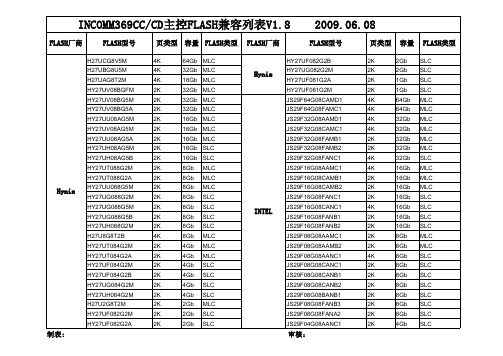
HY27UF082G2B
Hynix
HY27UG082G2M HY27UF081G2A HY27UF081G2M JS29F64G08CAMD1 JS29F64G08FAMC1 JS29F32G08AAMD1 JS29F32G08CAMC1 JS29F32G08FAMB1 JS29F32G08FAMB2 JS29F32G08FANC1 JS29F16G08AAMC1 JS29F16G08CAMB1 JS29F16G08CAMB2 JS29F16G08FANC1 JS29F16G08CANC1 JS29F16G08FANB1 JS29F16G08FANB2 JS29F08G08AAMC1 JS29F08G08AAMB2 JS29F08G08AANC1 JS29F08G08CANC1 JS29F08G08CANB1 JS29F08G08CANB2 JS29F08G08BANB1 JS29F08G08FANB3 JS29F08G08FANA2 JS29F04G08AANC1
FLASH厂商
容量
2Gb 2Gb 1Gb 1Gb 64Gb 64Gb 32Gb 32Gb 32Gb 32Gb 32Gb 16Gb 16Gb 16Gb 16Gb 16Gb 16Gb 16Gb 8Gb 8Gb 8Gb 8Gb 8Gb 8Gb 8Gb 8Gb 8Gb 4Gb
FLASH类型
SLC SLC SLC SLC MLC MLC MLC MLC MLC MLC SLC MLC MLC MLC SLC SLC SLC SLC MLC MLC SLC SLC SLC SLC SLC SLC SLC SLC
MICRON
MT29F4G08AAB MT29F4G08AAA MT29F2G08AAD MT29F2G08AAB MT29F2G08AAC MT29F2G08AAA K9HCG08U1M K9HCG08U5M K9LBG08U0M K9LBG08U1M K9HBG08U1M K9WBG08U1M K9GAG08U0M K9GAG08U0D K9LAG08U0M
NAND_Flash中文版资料
NAND Flash 存储器和使用ELNEC编程器烧录NAND Flash技术应用文档Summer 翻译整理深圳市浦洛电子科技有限公司August 2006目录一. 简介 ----------------------------------------------------------------------------------- 1 二. NAND Flash与NOR Flash的区别 -------------------------------------------- 1 三. NAND Flash存储器结构描叙 --------------------------------------------------- 4 四. 备用单元结构描叙 ---------------------------------------------------------------- 6 五. Skip Block method(跳过坏块方式) ------------------------------------------ 8 六. Reserved Block Area method(保留块区域方式)----------------------------- 9 七. Error Checking and Correction(错误检测和纠正)-------------------------- 10 八. 文件系统 ------------------------------------------------------------------------------10 九. 使用ELNEC系列编程器烧录NAND Flash -------------------------------- 10 十. Invalid Block Management drop-down menu -------------------------------- 12 十一. User Area Settings3 -------------------------------------------------------- 13 十二. Solid Area Settings --------------------------------------------------------- 15 十三. Quick Program Check-box ---------------------------------------------- 16 十四. Reserved Block Area Options --------------------------------------------17 十五. Spare Area Usage drop-down menu ------------------------------------18简介NAND Flash 结构最早是在1989年由日本东芝公司引入。
HY27UF081G2A NAND Flash数据手册

This document is a general product description and is subject to change without notice. Hynix does not assume any responsibility for use of circuits described. No patent licenses are implied.Rev 0.4 / Jun. 2007 1HY27UF(08/16)1G2A Series1Gbit (128Mx8bit / 64Mx16bit) NAND Flash1Gb NAND FLASHHY27UF081G2A HY27UF161G2ARev 0.4 / Jun. 200721Gbit (128Mx8bit / 64Mx16bit) NAND FlashDocument Title1Gbit (128Mx8bit / 64Mx16bit) NAND Flash Memory Revision HistoryRevision No.History Draft DateRemark0.01Initial Draft.Dec. 28. 2005Preliminary0.11) Change NOP2) Change AC CharacteristicsMay. 18. 2006Preliminary0.21) Delete Memory array map 2) Change AC Characteristics3) Correct copy back function Oct. 02. 2006Preliminary0.31) Change 1Gb Package Type- FBGA package is added - Figure & dimension are changed 2) Delet PreliminaryNov. 23. 20060.41) Correct figure 19Jun. 11. 2007tOH Before 12After10tCStCEA tREA Before 253525After202520Rev 0.4 / Jun. 200731Gbit (128Mx8bit / 64Mx16bit) NAND FlashFEATURES SUMMARYHIGH DENSITY NAND FLASH MEMORIES - Cost effective solutions for mass storage applications NAND INTERFACE - x8 or x16 bus width.- Multiplexed Address/ Data- Pinout compatibility for all densitiesSUPPLY VOLTAGE- VCC = 2.7 to 3.6V : HY27UFxx1G2A Memory Cell Array= (2K+64) Bytes x 64 Pages x 1,024 Blocks = (1K+32) Bytes x 64 Pages x 1,024 BlocksPAGE SIZE- x8 device : (2K+64 spare) Bytes : HY27UF081G2A - x16 device : (1K+32 spare) Bytes : HY27UF161G2ABLOCK SIZE- x8 device: (128K + 4K spare) Bytes - x16 device: (64K + 2K spare) Words PAGE READ / PROGRAM - Random access: 25us (max.) - Sequential access: 30ns (min.) - Page program time: 200us (typ.)COPY BACK PROGRAM MODE- Fast page copy without external bufferingCACHE PROGRAM- Internal (2048+64) Byte buffer to improve the program throughputFAST BLOCK ERASE- Block erase time: 2ms (Typ.)STATUS REGISTER ELECTRONIC SIGNATURE - 1st cycle: Manufacturer Code - 2nd cycle: Device Code- 3rd cycle: Internal chip number , Cell Type, Number of Simultaneously Programmed Pages.- 4th cycle: Page size, Block size, Organization, Spare sizeSERIAL NUMBER OPTION CHIP ENABLE DON’T CARE - Simple interface sith microcontrollerDATA RETENTION- 100,000 Program/Erase cycles (with 1bit/528byte ECC) - 10 years Data RetentionPACKAGE- HY27UF(08/16)1G2A-T(P): 48-Pin TSOP1 (12 x 20 x 1.2 mm)- HY27UF(08/16)1G2A-T (Lead)- HY27UF(08/16)1G2A-TP (Lead Free)- HY27UF081G2A-S(P): 48-Pin USOP1 (12 x 17 x 0.65 mm)- HY27UF081G2A-S (Lead)- HY27UF081G2A-SP (Lead Free) - HY27UF081G2A-F(P): 63-Ball FBGA (9 x 11 x 1.0 mm)- HY27UF081G2A-F (Lead)- HY27UF081G2A-FP (Lead Free)Rev 0.4 / Jun. 200741Gbit (128Mx8bit / 64Mx16bit) NAND Flash1. SUMMARY DESCRIPTIONThe Hynix HY27UF(08/16)1G2A series is a 128Mx8bit with spare 4Mx8 bit capacity. The device is offered in 3.3V Vcc Power Supply.Its NAND cell provides the most cost-effective solution for the solid state mass storage market. The memory is divided into blocks that can be erased independently so it is possible to preserve valid data while old data is erased.The device contains 1024 blocks, composed by 64 pages consisting in two NAND structures of 32 series connected Flash cells.A program operation allows to write the 2112-byte page in typical 200us and an erase operation can be performed in typical 2ms on a 128K-byte(X8 device) block.Data in the page can be read out at 30ns cycle time per byte. The I/O pins serve as the ports for address and data input/output as well as command input. This interface allows a reduced pin count and easy migration towards different densities, without any rearrangement of footprint.Commands, Data and Addresses are synchronously introduced using CE, WE, ALE and CLE input pin. The on-chip Pro-gram/Erase Controller automates all program and erase functions including pulse repetition, where required, and inter-nal verification and margining of data.The modify operations can be locked using the WP input pin or using the extended lock block feature described later .The output pin R/B (open drain buffer) signals the status of the device during each operation. In a system with multi-ple memories the R/B pins can be connected all together to provide a global status signal.Even the write-intensive systems can take advantage of the HY27UF(08/16)1G2A extended reliability of 100K pro-gram/erase cycles by providing ECC (Error Correcting Code) with real time mapping-out algorithm.The chip could be offered with the CE don’t care function. This function allows the direct download of the code from the NAND Flash memory device by a microcontroller , since the CE transitions do not stop the read operation.The copy back function allows the optimization of defective blocks management: when a page program operation fails the data can be directly programmed in another page inside the same array section without the time consuming serial data insertion phase.The cache program feature allows the data insertion in the cache register while the data register is copied into the flash array. This pipelined program operation improves the program throughput when long files are written inside the memory. A cache read feature is also implemented. This feature allows to dramatically improve the read throughput when consecutive pages have to be streamed out.The HYNIX HY27UF(08/16)1G2A series is available in 48 - TSOP1 12 x 20 mm, 48 - USOP 12 x 17 mmm, FBGA 9 x 11 mm.1.1 Product ListPART NUMBER ORIZATIONVCC RANGE PACKAGEHY27UF081G2A x8 2.7V - 3.6 Volt63FBGA / 48TSOP1 / 48USOP1HY27UF161G2Ax1648TSOP1Rev 0.4 / Jun. 200751Gbit (128Mx8bit / 64Mx16bit) NAND FlashIO15 - IO8Data Input / Outputs (x16 only)IO7 - IO0Data Inputs / Outputs CLE Command latch enable ALE Address latch enable CE Chip Enable RE Read Enable WE Write Enable WP Write Protect R/B Ready / Busy Vcc Power Supply Vss Ground NCNo ConnectionTable 1: Signal NamesRev 0.4 / Jun. 200761Gbit (128Mx8bit / 64Mx16bit) NAND FlashFigure 2. 48TSOP1 Contactions, x8 and x16 DeviceFigure 3. 48USOP1 Contactions, x8Rev 0.4 / Jun. 200771Gbit (128Mx8bit / 64Mx16bit) NAND FlashFigure 4. 63FBGA Contactions, x8 Device (Top view through package)Rev 0.4 / Jun. 200781Gbit (128Mx8bit / 64Mx16bit) NAND Flash1.2 PIN DESCRIPTIONPin Name DescriptionIO0-IO7IO8-IO15(1)DATA INPUTS/OUTPUTSThe IO pins allow to input command, address and data and to output data during read / program operations. The inputs are latched on the rising edge of Write Enable (WE). The I/O buffer float to High-Z when the device is deselected or the outputs are disabled.CLECOMMAND LATCH ENABLEThis input activates the latching of the IO inputs inside the Command Register on the Rising edge of Write Enable (WE).ALEADDRESS LATCH ENABLEThis input activates the latching of the IO inputs inside the Address Register on the Rising edge of Write Enable (WE).CECHIP ENABLEThis input controls the selection of the device. When the device is busy CE low does not deselect the memory.WEWRITE ENABLEThis input acts as clock to latch Command, Address and Data. The IO inputs are latched on the rise edge of WE.REREAD ENABLEThe RE input is the serial data-out control, and when active drives the data onto the I/O bus. Data is valid tREA after the falling edge of RE which also increments the internal column address counter by one.WP WRITE PROTECTThe WP pin, when Low, provides an Hardware protection against undesired modify (program / erase)operations.R/B READY BUSYThe Ready/Busy output is an Open Drain pin that signals the state of the memory.VCC SUPPLY VOLTAGEThe VCC supplies the power for all the operations (Read, Write, Erase). VSS GROUNDNCNO CONNECTIONTable 2: Pin DescriptionNOTE:1. A 0.1uF capacitor should be connected between the Vcc Supply Voltage pin and the Vss Ground pin to decouple the current surges from the power supply. The PCB track widths must be sufficient to carry the currents required during program and erase operations.Rev 0.4 / Jun. 200791Gbit (128Mx8bit / 64Mx16bit) NAND FlashIO0IO1IO2IO3IO4IO5IO6IO71st Cycle A0A1A2A3A4A5A6A72nd Cycle A8A9A10A11L (1)L (1)L (1)L (1)3rd Cycle A12A13A14A15A16A17A18A194th CycleA20A21A22A23A24A25A26A27Table 3: Address Cycle Map(x8)NOTE:1. L must be set to Low.IO0IO1IO2IO3IO4IO5IO6IO7IO8-IO151st Cycle A0A1A2A3A4A5A6A7L (1)2nd Cycle A8A9A10L (1)L (1)L (1)L (1)L (1)L (1)3rd Cycle A11A12A13A14A15A16A17A18L (1)4th CycleA19A20A21A22A23A24A25A26L (1)Table 4: Address Cycle Map(x16)NOTE:1. L must be set to Low.FUNCTION1st CYCLE2nd CYCLE3rd CYCLE4th CYCLEAcceptable commandduring busyREAD 100h 30h --READ FOR COPY-BACK 00h 35h --READ ID 90h ---RESETFFh ---YesPAGE PROGRAM 80h 10h --COPY BACK PGM 85h 10h --BLOCK ERASE60h D0h --READ STATUS REGISTER 70h ---YesCACHE PROGRAM 80h 15h --RANDOM DATA INPUT 85h ---RAMDOM DATA OUTPUT 05h E0h --CACHE READ START 00h 31h --CACHE READ EXIT34h---Table 5: Command SetRev 0.4 / Jun. 2007101Gbit (128Mx8bit / 64Mx16bit) NAND FlashCLE ALE CE WE RE WP MODE H L L Rising H X Read ModeCommand Input L H L Rising H X Address Input(4 cycles)H L L Rising H H Write ModeCommand Input L H L Rising H HAddress Input(4 cycles)L L L Rising H H Data Input L L L (1)H Falling X Sequential Read and Data Output L L L H H X During Read (Busy)X X X X X H During Program (Busy)X X X X X HDuring Erase (Busy)X X X X X L Write Protect XXHXX0V/Vcc Stand ByTable 6: Mode SelectionNOTE:1. With the CE high during latency time does not stop the read operationRev 0.4 / Jun. 2007111Gbit (128Mx8bit / 64Mx16bit) NAND Flash2. BUS OPERATIONThere are six standard bus operations that control the device. These are Command Input, Address Input, Data Input, Data Output, Write Protect, and Standby.Typically glitches less than 5 ns on Chip Enable, Write Enable and Read Enable are ignored by the memory and do not affect bus operations.2.1 Command Input.Command Input bus operation is used to give a command to the memory device. Command are accepted with Chip Enable low, Command Latch Enable High, Address Latch Enable low and Read Enable High and latched on the rising edge of Write Enable. Moreover for commands that starts a modify operation (write/erase) the Write Protect pin must be high. See figure 6 and table 13 for details of the timings requirements. Command codes are always applied on IO7:0, disregarding the bus configuration (X8/X16).2.2 Address Input.Address Input bus operation allows the insertion of the memory address. To insert the 28 addresses needed to access the 1Gbit 4 clock cycles (x8 version) are needed. Addresses are accepted with Chip Enable low, Address Latch Enable High, Command Latch Enable low and Read Enable High and latched on the rising edge of Write Enable. Moreover for commands that starts a modify operation (write/erase) the Write Protect pin must be high. See figure 7 and table 16 for details of the timings requirements. Addresses are always applied on IO7:0, disregarding the bus configuration (X8/X16).2.3 Data Input.Data Input bus operation allows to feed to the device the data to be programmed. The data insertion is serially and timed by the Write Enable cycles. Data are accepted only with Chip Enable low, Address Latch Enable low, Command Latch Enable low, Read Enable High, and Write Protect High and latched on the rising edge of Write Enable. See figure 8 and table 13 for details of the timings requirements.2.4 Data Output.Data Output bus operation allows to read data from the memory array and to check the status register content, the lock status and the ID data. Data can be serially shifted out toggling the Read Enable pin with Chip Enable low, Write Enable High, Address Latch Enable low, and Command Latch Enable low. See figures 9,10,12,13 and table 13 for details of the timings requirements.2.5 Write Protect.Hardware Write Protection is activated when the Write Protect pin is low. In this condition modify operation do not start and the content of the memory is not altered. Write Protect pin is not latched by Write Enable to ensure the pro-tection even during the power up.2.6 Standby.In Standby mode the device is deselected, outputs are disabled and Power Consumption is reduced.Rev 0.4 / Jun. 2007121Gbit (128Mx8bit / 64Mx16bit) NAND Flash3. DEVICE OPERATION3.1 Page Read.Upon initial device power up, the device defaults to Read mode. This operation is also initiated by writing 00h and 30h to the command register along with four address cycles. In two consecutive read operations, the second one does need 00h command, which four address cycles and 30h command initiates that operation. Second read operation always requires setup command if first read operation was executed using also random data out command.Two types of operations are available: random read. The random read mode is enabled when the page address is changed. The 2112 bytes (X8 device) or 1056 words (X16 device) of data within the selected page are transferred to the data registers in less than 25us(tR). The system controller may detect the completion of this data transfer (tR) by analyzing the output of R/B pin. Once the data in a page is loaded into the data registers, they may be read out in 30ns cycle time (3.3V device) by sequentially pulsing RE. The repetitive high to low transitions of the RE clock make the device output the data starting from the selected column address up to the last column address.The device may output random data in a page instead of the consecutive sequential data by writing randomdata output command. The column address of next data, which is going to be out, may be changed to the address which follows random data output command.Random data output can be operated multiple times regardless of how many times it is done in a page.Random data output is not available in cache read.3.2 Page Program.The device is programmed basically by page, but it does allow multiple partial page programming of a word or consec-utive bytes up to 2112 (X8 device) or words up to 1056 (X16 device), in a single page program cycle.The number of consecutive partial page programming operation within the same page without an intervening erase operation must not exceed 8; for example, 4 times for main array (X8 device:1time/512byte, X16 device:1time 256word) and 4 times for spare array (X8 device:1time/16byte ,X16 device:1time/8word).The addressing should be done in sequential order in a block. A page program cycle consists of a serial data loading period in which up to 2112 bytes (X8 device) or 1056 words (X16 device) of data may be loaded into the data register , followed by a non-volatile programming period where the loaded data is programmed into the appropriate cell.The serial data loading period begins by inputting the Serial Data Input command (80h), followed by the four cycle address inputs and then serial data. The words other than those to be programmed do not need to be loaded. The device supports random data input in a page. The column address of next data, which will be entered, may bechanged to the address which follows random data input command (85h). Random data input may be operated multi-ple times regardless of how many times it is done in a page.The Page Program confirm command (10h) initiates the programming process. Writing 10h alone without previously entering the serial data will not initiate the programming process. The P/E/R controller automatically executes the algorithms and timings necessary for program and verify, thereby freeing the system controller for other tasks. Once the program process starts, the Read Status Register command may be entered to read the status register . The system controller can detect the completion of a program cycle by monitoring the R/B output, or the Status bit (I/O 6) of the Status Register . Only the Read Status command and Reset command are valid while programming is in progress. When the Page Program is complete, the Write Status Bit (I/O 0) may be checked. The internal write verify detects only errors for "1"s that are not successfully programmed to "0"s. The command register remains in Read Status command mode until another valid command is written to the command register . Figure 14 details the sequence.Rev 0.4 / Jun. 2007131Gbit (128Mx8bit / 64Mx16bit) NAND Flash3.3 Block Erase.The Erase operation is done on a block basis. Block address loading is accomplished in two cycles initiated by an Erase Setup command (60h). Only address A18 to A27 (X8) or A17 to A26 (X16) is valid while A12 to A17 (X8) or A11 to A16 (X16) are ignored. The Erase Confirm command (D0h) following the block address loading initiates the internal erasing process. This two-step sequence of setup followed by execution command ensures that memory contents are not acci-dentally erased due to external noise conditions. At the rising edge of WE after the erase confirm command input, the P/E/R controller handles erase and erase-verify. Once the erase process starts, the Read Status Register command may be entered to read the status register . The system controller can detect the completion of an erase by monitoring the R/B output, or the Status bit (I/O 6) of the Status Register . Only the Read Status command and Reset command are valid while erasing is in progress. When the erase operation is completed, the Write Status Bit (I/O 0) may be checked. Figure 18 details the sequence.3.4 Copy-Back Program.The copy-back program is configured to quickly and efficiently rewrite data stored in one page without utilizing an exter-nal memory. Since the time-consuming cycles of serial access and re-loading cycles are removed, the system perfor-mance is improved. The benefit is especially obvious when a portion of a block is updated and the rest of the block also need to be copied to the newly assigned free block. The operation for performing a copy-back program is a sequential execution of page-read without serial access and copyingprogram with the address of destination page. A read opera-tion with "35h" command and the address of the source page moves the whole 2112byte (X8 device) or 1056word (X16 device) data into the internal data buffer .As soon as the device returns to Ready state, Copy Back command (85h) with the address cycles of destination page may be written. The Program Confirm command (10h) is required to actually begin the programming operation. Data input cycle for modifying a portion or multiple distant portions of the source page is allowed as shown in Figure 16."When there is a program-failure at Copy-Back operation, error is reported by pass/fail status. But, if Copy-Back operations are accumulated over time, bit error due to charge loss is not checked by external error detection/correction scheme. For this reason, two bit error correction is recommended for the use of Copy-Back operation."Figure 16 shows the command sequence for the copy-back operation.The Copy Back Program operation requires three steps:1. The source page must be read using the Read A command (one bus write cycle to setup the command and then 4 bus write cycles to input the source page address). This operation copies all 2KBytes from the page into the Page Buffer .2. When the device returns to the ready state (Ready/Busy High), the second bus write cycle of the command is given with the 4bus cycles to input the target page address.3. Then the confirm command is issued to start the P/E/R Controller .Note:1. On the same plane.2. It’s prohibited to operate copy-back program from an odd address page (source page) to an even address page (target page) or from an even address page (source page) to an odd address page (target page). Therefore, the copy-back program is permitted just between odd address pages or even address pages.Rev 0.4 / Jun. 2007141Gbit (128Mx8bit / 64Mx16bit) NAND Flash3.5 Read Status Register.The device contains a Status Register which may be read to find out whether read, program or erase operation is com-pleted, and whether the program or erase operation is completed successfully. After writing 70h command to the com-mand register , a read cycle outputs the content of the Status Register to the I/O pins on the falling edge of CE or RE, whichever occurs last. This two line control allows the system to poll the progress of each device in multiple memory connections even when R/B pins are common-wired. RE or CE does not need to be toggled for updated status. Refer to Table 14 for specific Status Register definitions, and Figure 10 for specific timings requirements . The command reg-ister remains in Status Read mode until further commands are issued to it. Therefore, if the status register is read dur-ing a random read cycle, the read command (00h) should be given before starting read cycles.3.6 Read ID.The device contains a product identification mode, initiated by writing 90h to the command register , followed by an address input of 00h. Four read cycles sequentially output the 1st cycle (ADh), and 2nd cycle (the device code) and 3rd cycle ID, 4th cycle ID, respectively. The command register remains in Read ID mode until further commands are issued to it. Figure 19 shows the operation sequence, while Tables 16 explain the byte meaning.3.7 Reset.The device offers a reset feature, executed by writing FFh to the command register . When the device is in Busy state during random read, program or erase mode, the reset operation will abort these operations. The contents of memory cells being altered are no longer valid, as the data will be partially programmed or erased.The command register is cleared to wait for the next command, and the Status Register is cleared to value E0h when WP is high. Refer to table 14 for device status after reset operation. If the device is already in reset state a new reset command will not be accepted by the command register . The R/B pin transitions to low for tRST after the Reset com-mand is written.Rev 0.4 / Jun. 2007151Gbit (128Mx8bit / 64Mx16bit) NAND Flash3.8 Cache programCache Program is an extension of Page Program, which is executed with 2112byte (X8 device) or 1056word (X16 device) data registers, and is available only within a block. Since the device has 1 page of cache memory, serial data input may be executed while data stored in data register are programmed into memory cell. After writing the first set of data up to 2112byte (X8 device) or 1056word (X16 device) into the selected cache registers, Cache Program com-mand (15h) instead of actual Page Program (10h) is input to make cache registers free and to start internal program operation. To transfer data from cache registers to data registers, the device remains in Busy state for a short period of time (tCBSY) and has its cache registers ready for the next data-input while the internal programming gets started with the data loaded into data registers. Read Status command (70h) may be issued to find out when cache registers become ready by polling the Cache- Busy status bit (I/O 6). Pass/fail status of only the previous page is available upon the return to Ready state.When the next set of data is input with the Cache Program command, tCBSY is affected by the progress of pending internal programming. The programming of the cache registers is initiated only when the pending program cycle is finished and the data registers are available for the transfer of data from cache registers. The status bit (I/O5) for internal Ready/Busy may be polled to identify the completion of internal programming.If the system monitors the progress of programming only with R/B, the last page of the target programming sequence must be programmed with actual Page Program command (10h). If the Cache Program command (15h) is used instead, status bit (I/O5) must be polled to find out when the last programming is actually finished before starting other operations such as read. Pass/fail status is available in two steps. I/O 1 returns with the status of the previous page upon Ready or I/O6 status bit changing to "1", and later I/O 0 with the status of current page upon true Ready (returning from internal programming) or I/O 5 status bit changing to "1". I/O 1 may be read together when I/O 0 is checked. See Fig. 18 for more details.NOTE : Since programming the last page does not employ caching, the program time has to be that of Page Program. However , if the previous program cycle with the cache data has not finished, the actual program cycle of the last page is initiated only after completion of the previous cycle, which can be expressed as the following formula.tPROG=Program time for the last page + Program time for the (last-1)page - (Program command cycle time + Last page data loading time)Rev 0.4 / Jun. 2007161Gbit (128Mx8bit / 64Mx16bit) NAND Flash3.9 Cache ReadCache read operation allows automatic download of consecutive pages, up to the whole device. Immediately after 1st latency end, while user can start reading out data, device internally starts reading following page.Start address of 1st page must be at page start (A<10:0>=00h) : in this way after 1st latency time (tr) , automatic data download will be uninterrupted. In fact latency time is 25us, while download of a page require at least 100us for x8 device (50us for x16 device).Cache read operation command is like standard read, except for confirm code (30h for standard read, 31h for cache read) user can check operation status using :- R/B ( ‘0’ means latency ongoing, download not possible, ‘1’ means download of n page possible, even if device in ternally is active on n+1 page- Status register (SR<6> behave like R/B, SR<5> is ‘0’ when device is internally reading and ‘1’ when device is idle)To exit cache read operation, a cache read exit command (34h) must be issued. This command can be given any time (both device idle and reading).If device is active (SR<5>=0) it will go idle within 5us, while if it is not active, device itself will go busy for a time shorter then tCBSY before becoming again idle and ready to accept any further commands. Figure 17 describes how to handle Cache Read through Status register .If user reads last byte/word of the memory array, then he has to stop by giving a cache read exit command. In general,if user wants to terminate a cache read, then he must give a cache read exit command (or reset command) before starting any new operation.Random data output is not available in cache read.Cache read operation must be done only block by block if system needs to avoid reading also from invalid blocks.Rev 0.4 / Jun. 2007171Gbit (128Mx8bit / 64Mx16bit) NAND Flash4. OTHER FEATURES4.1 Data Protection for Power on/off SequenceThe device is designed to offer protection from any involuntary program/erase during power-transitions. An internal voltage detector disables all functions whenever Vcc is below about 2.0V (3.3V version). WP pin provides hardware protection and is recommended to be kept at VIL during power-up and power-down. A recovery time of minimum 10us is required before internal circuit gets ready for any command sequences as shown in Figure 24. The two-step com-mand sequence for program/erase provides additional software protection.If the power is dropped during the ready read/write/erase operation, Power protection function may not guaranteed the data. Power protection function is only available during the power on/off sequence.4.2 Ready/Busy.The device has a Ready/Busy output that provides method of indicating the completion of a page program, erase, copy-back, cache program and random read completion. The R/B pin is normally high and goes to low when the device is busy (after a reset, read, program, erase operation). It returns to high when the P/E/R controller has finished the operation. The pin is an open-drain driver thereby allowing two or more R/B outputs to be Or-tied. Because pull-up resistor value is related to tr(R/B) and current drain during busy (Ibusy), an appropriate value can be obtained with the following reference chart (Figure 25). Its value can be determined by the following guidance.。
20-STM32CubeMX系列教程20-Nand Flash

/* Erase the NAND first Block */ HAL_NAND_Erase_Block(&hnand1,&WriteReadAddr);
/* Fill the buffer to send */ for (i = 0; i < NAND_PAGE_SIZE; i++ ) {
TxBuffer[i] = i; }
下面为发送命令的时序图,已经对应的时间参数表:
用 FMC 控制 Nand Flash 我们只需要知道访问波形图中的四个时间参数既可。 从上这三个图我们可以知道:
MEMxSET = tCLS - tWP >= 0ns MEMxWAIT = tWP >= 12ns MEMxHOLED = tCLH >= 5ns MEMxHIZ = tCLS - tDS >= 0ns 六、新建工程 复制串口 printf 的工程,修改文件夹名。击 STM32F746I.ioc 打开 STM32cubeMX 的工程文件 重新配置,选择 NCE3 开启 NAND Flash,数据地址线选择 8 bits,Ready or Busy 选择 NWAIT。
NOR Flash:允许随机存取存储器上的任何区域,以编码应用为主,其功能多与运算相关 Nand Flash:主要功能是存储资料,适合储存卡之类的大量数据的存储。
U盘 维修
U盘(优盘)的故障表现及数据恢复1、U盘毫无反应:有可能U盘插口针脚断裂,晶震坏,稳压三极管电路不能工作,数据全部可以恢复。
2。
有盘符,提示请插入磁盘:<1>U盘主控内部系统文件损坏,数据全部可以恢复。
一般更换相同的主控即可,可是找一个相同的U 盘,主控相同,U盘容量相同,实在不易,为此我公司引进世界先进技术,直接读取FLASH芯片内的数据,达到快速恢复文件,欢迎咨询<2>U盘FLASH芯片存在坏块区,数据恢复可以完全恢复或部份恢复,视具体损坏情况来定!3。
有盘符但提示未格式化:U盘存在坏扇区或引导扇区有问题,如无重要数据格式化之后便可使用。
可做数据恢复,而且数据恢复的结果十分完整,这种情况一般都是使用不当造成的故障,如热插拔之类的误操作,USB接口电压等,尽量使用时正常使用。
4。
无盘符提示无法识别的USB设备:晶震或稳压三极管损坏,这种情况数据全部可以恢复。
5。
逻辑类的问题:无盘符,但能检到U盘,提示格式化等,数据可以恢复。
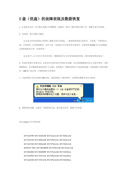
常见flash芯片类型列表H27UCG8VFM HY27UG088G5M HY27SA161G1M HY27SS08121MH27U2G8T2M HY27UH08AG5M HY27UF081G2A HY27SS16121MH27U2G8T2M HY27UH08AG5B HY27UF161G2A HY27US08121MHN29V2G74W30 HY27UK08BGFM HY27UF081G2M HY27US16121MH27UBG8H5M HY27UH08BGFB HY27UF161G2M HY27US08561AH27U8G8F2M HY27UT084G2A HY27SF081G2M HY27US16561AH27UAG8G5M HY27UT084G2M HY27SF161G2M HY27SS08561AH27UBG8T5M HY27UU088G5M HY27UF082G2A HY27SS16561AHY27US08281A HY27UT088G2M HY27UF162G2A HY27US08561MHY27US08561A HY27UT088G2A HY27UF082G2B HY27US16561MHY27US08561M HY27UV08AG5M HY27UF162G2B HY27SS08561MHY27US08121A HY27UV08BG5M HY27UF084G2B HY27SS16561MHY27US08121M HY27UV08BGFM HY27UF164G2B HY27US08281AHY27UA081G1M HY27UV08BGFA HY27UF082G2M HY27US16281AHY27UA081G4M HY27UU08AG5M HY27UF162G2M HN29W12811T-60HY27UB082G4M HY27UU08AG5A HY27UH088G2M HN29V25691BTHY27UF081G2A HY27UW08BGFM HY27UH088GDM HN29V51211T-50HY27UF081G2M HY27UW08CGFM HY27UG088G5B HN29V1G91T-30HY27UF082G2A Hynix InkDie HY27UG088G5M HY27UF164G2B(x16)HY27UF082G2M H27UAG8T2M HY27UH08AG5M HYF33DS512804(5)BTC HY27UF082G2B H27UCG8V5M HY27UK08BGFM HYF33DS512804(5)BTC HY27UF084G2B HY27SF082G2B HY27US081G1M HYF33DS512804(5)BTC HY27UG088G5B HY27SF162G2B HY27US161G1M HYF33DS512804(5)BTC HY27UF084G2M HY27SF081G2A HY27US08121A HYF33DS1G800CTIHY27UG084G2M HY27SF161G2A HY27US16121A HYF33DS1G800CTIHY27UH084G2M HY27U(s)A081G1M HY27SS08121A HY27US16562AHY27UH088G2M HY27UA161G1M HY27SS16121A HY27SS081G1XI29F04G08AAA I29F32G08CAMCI FTGM40A2GK3WG FTNL41B8GK3PGI29F08G08AAMB2 I29F64G08FAMC1 FBNL41B32K3P4 FTNL41B8GK3PGI29F08G08AAMBI PF79BL1208BSG FBNL41B8GK3P2 FTNL41B8GK3PGI29F16G08AAMCI PF79AL1208BS FTNL41BHGK3W4 R1FV04G13RSA-3I29F16G08MAA DFT512W08B-P1 FBNL41B8GK3W3 R1FV04G13RSA-3_2ASU4GA30GT K9F2G08U0M K9WBG08U1M K9L8G08U0MASU2GA30GT K9F2G08U0M K9NBG08U5A K9LAG08U0MK9F2808U0B K9K2G08U0M K9NCG08U5M K9LAG08U0A_BK9F5608U0B K9GAG08U0A K9G2G08U0M K9HBG08U1AK9F1208U0A K9GAG08U0D K9G4G08U0A K9LBG08U0MK9F1208U0B K9K4G08U0M K9G8G08U0A K9HAG08U1MK9F1208U0C K9F4G08U0A K9G8G08U0M K9HBG08U1MK9K1G08U0M K9F8G08U0M K9L8G08U1M K9HCG08U1MK9E2G08U1M K9K8G08U0A K9LBG08U0D K9MDG08U5MK9F1G16U0M K9KAG08U0M K9HCG08U1M K9MBG08U5MK9F1G08U0A K9W8G08U1M K9HCG08U1D K9MCG08U5MK9F1G08U0B K9WAG08U1A K9LAG08U1M K9GAG08U0MK9F1G08U0M K9LBG08U1M K9HCG08U5M K9F5616U0C(x16)K9F2G08U0A K9F1208U0M K9F5616U0C K9K4G16Q0MK9F1G16Q0M K9F2808U0 K9G8G08U0M K9XXG08UXMK9F1G08 K9F5608U0B K9LAG08U0M K9K4G16U0MK9F1G16U0M K9F5616U0B K9HBG08U1M K9K8G08U0MK9F2G08U0A K9F5608D0C K9MCG08U5M K9WAG08U1MK9F2G16U0M K9F5616D0C K9K1G08U0M K9K2G08Q0MK9F2G08U0M K9F5608U0C K9K4G08Q0M K9K2G16Q0MK9XXG08UXM K9XXG16UXM K9K2G08U0M K9F1G08Q0MNAND128W3A2BN6E NAND08GW3C2B NAND512R3A NAND04GW4B2DNAND256W3A2BN6E NAND16GW3C4B NAND512W3A NAND08GW3B2CNAND512W3A0AN6 NAND01GW3B2B NAND512R4A NAND08GR4B2CNAND01GW3A0AN6 NAND01GR4B2B NAND512W4A NAND08GW4B2CNAND01GW3B2AN6 NAND01GW4B2B NAND01GR3A NAND08GW3C2ANAND01GW3B2BN6 NAND02GW3B2C NAND01GW3A NAND16GW3C4ANAND02GW3B2AN6 NAND02GR4B2C NAND01GR4A NAND08GW3C2BNAND02GW3B2D NAND02GW4B2C NAND01GW4A NAND08GW3D2ANAND02GW3B2CN6 NAND01GW3B2C NAND02GW3B2D NAND512R3A2DNAND04GW3B2DN6 NAND01GR4B2C NAND02GR4B2D NAND512W3A2DNAND04GW3B2BN6 NAND01GW4B2C NAND02GW4B2D NAND512R4A2DNAND08GW3B2CN6 NAND128R3A NAND04GW3C2A NAND512W4A2DNAND08GW3B2AN6 NAND128W3A NAND04GA3C2A NAND01GR3A2CNAND04GW3C2AN1 NAND256R3A NAND04GW3B2B NAND01GW3A2CNAND08GW3C2AN1 NAND256W3A NAND08GW3B2A NAND01GR4A2CNAND08GW3B2CN6 NAND256R4A NAND04GW3B2D NAND01GW4A2CNAND04GW3C2B NAND256W4A NAND04GR4B2D NAND04GW3C2BNAND08GW3F2A NAND16GW3F2A NAND08GW3C2BMT29F8G08MAA MT29F64G08TAA MT29F4G08ABC MT29F4G08BABMT29F8G16MAA MT29F32G08BAAA MT29F32G08FAA MT29F8G08FABMT29F16G08QAA MT29F64G08CFAAA MT29F8G08BAA MT29F4G16BABMT29F2G08AAC MT29F4G08ABC MT29F8G08DAA MT29F16G08QAA(DUAL) MT29F32G08TAA MT29F2G08AAA MT29F16G08FAA MT29F2G08ABCMT29F2G16AAC MT29F2G16ABD MT29F4G08MAA MT29F32G08TAA-BMT29F2G16ABC MT29F2G08AAB_C MT29F4G08MAA_2 MT29F128G08CJAAA MT29F4G08BBC MT29F4G08AAA_C MT29F8G08MAD MT29F4G08BACMT29F8G08MBD MT29F4G08BAB_C MT29F8G08MAD MT29F8G08FACMT29F4G08AAA MT29F8G08FAB_C MT29F2G08AAD MT29F16G08CBABAMT29F8G08DAA MT29F8G08MAD MT29F2G08AAB MT29F32G08CBABAMT29F16G08MAA MT29F8G08AAA MT29F2G08ABB MT29F8G08BAAMT29F16G08MAA MT29F16G08DAA MT29F2G16AAB MT29F16G08FAAMT29F32G08QAA MT29F2G08ABC MT29F2G16ABBSDTNFCH-512 SDTNKGHSM-8192 SDMLC-1GB-I SDUNIHHSM-8192(16bit)SDTNFCH-1024 SDMLC-16384-I SDTNLLBHSM-32768 SDTNIHHSM-4096(16Bit)SDTNKGHSM-1024 SDTNKHHSM-16384 SANDISK-16384(43nm) SDTNKGHSM-4096(16bit) SDTNGBHE0-2048-I SDTNKHHSM-32768 SDTNIGHE0-4096 SDTNKHHSM-32768(16bit)SDTNGFHE0-2048 SDTNLJCHSM-2048 Sandisk-4GB(43nm) SDTNLLAHSM-1024(16bit) SDTNKGHSM-2048 SDTNLJCHSM-4096 SDTNLMBHSM-4096 SDTNKGHSM-2048(16bit)SDMLC-4GB-I SM90-256MB SDTNKLBHSM-2048 SDTNKJBHSM-8192(16bit)SDTNKGHSM-4096 SM90-256MB SDTNLLCHSM-1024 SDTNKGHSM-8192(16bit)SDTNLJCHSM-1024 SDTNIGHSM-2048 SDTNLLBHSM-4096 SDTNIGHSM-4096(16bit)SDUNIHHSM-8192 SDTNIGHSM-2048(16bit) SDMLC-1GB-I SDTNKHHSM-16384(16bit) SDTNIHHSM-4096 SDMLC-2GB-I SDTNKHHSM-16384(16bit)TC58NVG4D1DTG00 TC58NVG3D4CTG00 TC58DVG14B1FT00 TC58DVG02ATC58NVG4D2ETA00 TC58DVM72A1FT00 TC58NVG1D4BTG00 TC58DVM92ATH58NVG4D6CTG00 TC58DVM82A1FT00 TH58DVG24B1FT00 TC58NVG0S3CTA00TH58NVG6D1DTG20 TC58DVM92A1FT00 TC58NVG2D4BFT00 TC58NVM9S3BTG00TH58NVG5D2ETA20 TC58DVG02A1FT00 TH58NVG3D4BTG00 TC58NVG3D1DTG00(S)TH58NVG6D2ETA20 TC58NVG02A2FT00 TC58NVG3D4CTG10 TC58NVG6D1DTG00TH58NVG4T2DTG00 TC58NVG0S3BTG00 TH58NVG4D4CTG00 TC58NVG7D1DTG20TH58NVG6T2DTG20 TC58NVG1S3BTG00 TH58NVG5D4CTG20 TC58NVG2D1DTG00TH58NVG5D2ETA00 TH58NVG2S3BFT00 TC58NVG3D1DTG00 TC58NVG2D1DTG00TH58NVG5D1DTG00 TC58DVM94B1FT00 TH58NVG6D1DTG80 TC58NVG5D1DTG20TC58512FT TC58DVG04B1FT00 TC58NVG4D1DTG00工厂级U盘维修很多人打电话咨询U盘故障及数据恢复问题,现在把U盘的一些故障及排除方法归类一、硬件故障故障现象:U盘插在电脑里面什么反应都没有或是插上去在设备管理器的“通用串行总线控制器”里面能看到有新设备,但是我的电脑里面没有出现新盘符此类故障必须要懂电子的人才能搞定,至少要懂得焊接故障排除:重新焊好FLASH和主控,如果有新晶振也可以换掉试下,如果还不行就只有换主控IC了,总之,至少插在电脑里面要有新的盘符显示才算硬件基本正常(不是完全正常哦)。
- 1、下载文档前请自行甄别文档内容的完整性,平台不提供额外的编辑、内容补充、找答案等附加服务。
- 2、"仅部分预览"的文档,不可在线预览部分如存在完整性等问题,可反馈申请退款(可完整预览的文档不适用该条件!)。
- 3、如文档侵犯您的权益,请联系客服反馈,我们会尽快为您处理(人工客服工作时间:9:00-18:30)。
This document is a general product description and is subject to change without notice. Hynix does not assume any responsibility for use of circuits described. No patent licenses are implied.Rev 0.4 / Jun. 2007 1HY27UF(08/16)1G2A Series1Gbit (128Mx8bit / 64Mx16bit) NAND Flash1Gb NAND FLASHHY27UF081G2A HY27UF161G2ARev 0.4 / Jun. 200721Gbit (128Mx8bit / 64Mx16bit) NAND FlashDocument Title1Gbit (128Mx8bit / 64Mx16bit) NAND Flash Memory Revision HistoryRevision No.History Draft DateRemark0.01Initial Draft.Dec. 28. 2005Preliminary0.11) Change NOP2) Change AC CharacteristicsMay. 18. 2006Preliminary0.21) Delete Memory array map 2) Change AC Characteristics3) Correct copy back function Oct. 02. 2006Preliminary0.31) Change 1Gb Package Type- FBGA package is added - Figure & dimension are changed 2) Delet PreliminaryNov. 23. 20060.41) Correct figure 19Jun. 11. 2007tOH Before 12After10tCStCEA tREA Before 253525After202520Rev 0.4 / Jun. 200731Gbit (128Mx8bit / 64Mx16bit) NAND FlashFEATURES SUMMARYHIGH DENSITY NAND FLASH MEMORIES - Cost effective solutions for mass storage applications NAND INTERFACE - x8 or x16 bus width.- Multiplexed Address/ Data- Pinout compatibility for all densitiesSUPPLY VOLTAGE- VCC = 2.7 to 3.6V : HY27UFxx1G2A Memory Cell Array= (2K+64) Bytes x 64 Pages x 1,024 Blocks = (1K+32) Bytes x 64 Pages x 1,024 BlocksPAGE SIZE- x8 device : (2K+64 spare) Bytes : HY27UF081G2A - x16 device : (1K+32 spare) Bytes : HY27UF161G2ABLOCK SIZE- x8 device: (128K + 4K spare) Bytes - x16 device: (64K + 2K spare) Words PAGE READ / PROGRAM - Random access: 25us (max.) - Sequential access: 30ns (min.) - Page program time: 200us (typ.)COPY BACK PROGRAM MODE- Fast page copy without external bufferingCACHE PROGRAM- Internal (2048+64) Byte buffer to improve the program throughputFAST BLOCK ERASE- Block erase time: 2ms (Typ.)STATUS REGISTER ELECTRONIC SIGNATURE - 1st cycle: Manufacturer Code - 2nd cycle: Device Code- 3rd cycle: Internal chip number , Cell Type, Number of Simultaneously Programmed Pages.- 4th cycle: Page size, Block size, Organization, Spare sizeSERIAL NUMBER OPTION CHIP ENABLE DON’T CARE - Simple interface sith microcontrollerDATA RETENTION- 100,000 Program/Erase cycles (with 1bit/528byte ECC) - 10 years Data RetentionPACKAGE- HY27UF(08/16)1G2A-T(P): 48-Pin TSOP1 (12 x 20 x 1.2 mm)- HY27UF(08/16)1G2A-T (Lead)- HY27UF(08/16)1G2A-TP (Lead Free)- HY27UF081G2A-S(P): 48-Pin USOP1 (12 x 17 x 0.65 mm)- HY27UF081G2A-S (Lead)- HY27UF081G2A-SP (Lead Free) - HY27UF081G2A-F(P): 63-Ball FBGA (9 x 11 x 1.0 mm)- HY27UF081G2A-F (Lead)- HY27UF081G2A-FP (Lead Free)Rev 0.4 / Jun. 200741Gbit (128Mx8bit / 64Mx16bit) NAND Flash1. SUMMARY DESCRIPTIONThe Hynix HY27UF(08/16)1G2A series is a 128Mx8bit with spare 4Mx8 bit capacity. The device is offered in 3.3V Vcc Power Supply.Its NAND cell provides the most cost-effective solution for the solid state mass storage market. The memory is divided into blocks that can be erased independently so it is possible to preserve valid data while old data is erased.The device contains 1024 blocks, composed by 64 pages consisting in two NAND structures of 32 series connected Flash cells.A program operation allows to write the 2112-byte page in typical 200us and an erase operation can be performed in typical 2ms on a 128K-byte(X8 device) block.Data in the page can be read out at 30ns cycle time per byte. The I/O pins serve as the ports for address and data input/output as well as command input. This interface allows a reduced pin count and easy migration towards different densities, without any rearrangement of footprint.Commands, Data and Addresses are synchronously introduced using CE, WE, ALE and CLE input pin. The on-chip Pro-gram/Erase Controller automates all program and erase functions including pulse repetition, where required, and inter-nal verification and margining of data.The modify operations can be locked using the WP input pin or using the extended lock block feature described later .The output pin R/B (open drain buffer) signals the status of the device during each operation. In a system with multi-ple memories the R/B pins can be connected all together to provide a global status signal.Even the write-intensive systems can take advantage of the HY27UF(08/16)1G2A extended reliability of 100K pro-gram/erase cycles by providing ECC (Error Correcting Code) with real time mapping-out algorithm.The chip could be offered with the CE don’t care function. This function allows the direct download of the code from the NAND Flash memory device by a microcontroller , since the CE transitions do not stop the read operation.The copy back function allows the optimization of defective blocks management: when a page program operation fails the data can be directly programmed in another page inside the same array section without the time consuming serial data insertion phase.The cache program feature allows the data insertion in the cache register while the data register is copied into the flash array. This pipelined program operation improves the program throughput when long files are written inside the memory. A cache read feature is also implemented. This feature allows to dramatically improve the read throughput when consecutive pages have to be streamed out.The HYNIX HY27UF(08/16)1G2A series is available in 48 - TSOP1 12 x 20 mm, 48 - USOP 12 x 17 mmm, FBGA 9 x 11 mm.1.1 Product ListPART NUMBER ORIZATIONVCC RANGE PACKAGEHY27UF081G2A x8 2.7V - 3.6 Volt63FBGA / 48TSOP1 / 48USOP1HY27UF161G2Ax1648TSOP1Rev 0.4 / Jun. 200751Gbit (128Mx8bit / 64Mx16bit) NAND FlashIO15 - IO8Data Input / Outputs (x16 only)IO7 - IO0Data Inputs / Outputs CLE Command latch enable ALE Address latch enable CE Chip Enable RE Read Enable WE Write Enable WP Write Protect R/B Ready / Busy Vcc Power Supply Vss Ground NCNo ConnectionTable 1: Signal NamesRev 0.4 / Jun. 200761Gbit (128Mx8bit / 64Mx16bit) NAND FlashFigure 2. 48TSOP1 Contactions, x8 and x16 DeviceFigure 3. 48USOP1 Contactions, x8Rev 0.4 / Jun. 200771Gbit (128Mx8bit / 64Mx16bit) NAND FlashFigure 4. 63FBGA Contactions, x8 Device (Top view through package)Rev 0.4 / Jun. 200781Gbit (128Mx8bit / 64Mx16bit) NAND Flash1.2 PIN DESCRIPTIONPin Name DescriptionIO0-IO7IO8-IO15(1)DATA INPUTS/OUTPUTSThe IO pins allow to input command, address and data and to output data during read / program operations. The inputs are latched on the rising edge of Write Enable (WE). The I/O buffer float to High-Z when the device is deselected or the outputs are disabled.CLECOMMAND LATCH ENABLEThis input activates the latching of the IO inputs inside the Command Register on the Rising edge of Write Enable (WE).ALEADDRESS LATCH ENABLEThis input activates the latching of the IO inputs inside the Address Register on the Rising edge of Write Enable (WE).CECHIP ENABLEThis input controls the selection of the device. When the device is busy CE low does not deselect the memory.WEWRITE ENABLEThis input acts as clock to latch Command, Address and Data. The IO inputs are latched on the rise edge of WE.REREAD ENABLEThe RE input is the serial data-out control, and when active drives the data onto the I/O bus. Data is valid tREA after the falling edge of RE which also increments the internal column address counter by one.WP WRITE PROTECTThe WP pin, when Low, provides an Hardware protection against undesired modify (program / erase)operations.R/B READY BUSYThe Ready/Busy output is an Open Drain pin that signals the state of the memory.VCC SUPPLY VOLTAGEThe VCC supplies the power for all the operations (Read, Write, Erase). VSS GROUNDNCNO CONNECTIONTable 2: Pin DescriptionNOTE:1. A 0.1uF capacitor should be connected between the Vcc Supply Voltage pin and the Vss Ground pin to decouple the current surges from the power supply. The PCB track widths must be sufficient to carry the currents required during program and erase operations.Rev 0.4 / Jun. 200791Gbit (128Mx8bit / 64Mx16bit) NAND FlashIO0IO1IO2IO3IO4IO5IO6IO71st Cycle A0A1A2A3A4A5A6A72nd Cycle A8A9A10A11L (1)L (1)L (1)L (1)3rd Cycle A12A13A14A15A16A17A18A194th CycleA20A21A22A23A24A25A26A27Table 3: Address Cycle Map(x8)NOTE:1. L must be set to Low.IO0IO1IO2IO3IO4IO5IO6IO7IO8-IO151st Cycle A0A1A2A3A4A5A6A7L (1)2nd Cycle A8A9A10L (1)L (1)L (1)L (1)L (1)L (1)3rd Cycle A11A12A13A14A15A16A17A18L (1)4th CycleA19A20A21A22A23A24A25A26L (1)Table 4: Address Cycle Map(x16)NOTE:1. L must be set to Low.FUNCTION1st CYCLE2nd CYCLE3rd CYCLE4th CYCLEAcceptable commandduring busyREAD 100h 30h --READ FOR COPY-BACK 00h 35h --READ ID 90h ---RESETFFh ---YesPAGE PROGRAM 80h 10h --COPY BACK PGM 85h 10h --BLOCK ERASE60h D0h --READ STATUS REGISTER 70h ---YesCACHE PROGRAM 80h 15h --RANDOM DATA INPUT 85h ---RAMDOM DATA OUTPUT 05h E0h --CACHE READ START 00h 31h --CACHE READ EXIT34h---Table 5: Command SetRev 0.4 / Jun. 2007101Gbit (128Mx8bit / 64Mx16bit) NAND FlashCLE ALE CE WE RE WP MODE H L L Rising H X Read ModeCommand Input L H L Rising H X Address Input(4 cycles)H L L Rising H H Write ModeCommand Input L H L Rising H HAddress Input(4 cycles)L L L Rising H H Data Input L L L (1)H Falling X Sequential Read and Data Output L L L H H X During Read (Busy)X X X X X H During Program (Busy)X X X X X HDuring Erase (Busy)X X X X X L Write Protect XXHXX0V/Vcc Stand ByTable 6: Mode SelectionNOTE:1. With the CE high during latency time does not stop the read operationRev 0.4 / Jun. 2007111Gbit (128Mx8bit / 64Mx16bit) NAND Flash2. BUS OPERATIONThere are six standard bus operations that control the device. These are Command Input, Address Input, Data Input, Data Output, Write Protect, and Standby.Typically glitches less than 5 ns on Chip Enable, Write Enable and Read Enable are ignored by the memory and do not affect bus operations.2.1 Command Input.Command Input bus operation is used to give a command to the memory device. Command are accepted with Chip Enable low, Command Latch Enable High, Address Latch Enable low and Read Enable High and latched on the rising edge of Write Enable. Moreover for commands that starts a modify operation (write/erase) the Write Protect pin must be high. See figure 6 and table 13 for details of the timings requirements. Command codes are always applied on IO7:0, disregarding the bus configuration (X8/X16).2.2 Address Input.Address Input bus operation allows the insertion of the memory address. To insert the 28 addresses needed to access the 1Gbit 4 clock cycles (x8 version) are needed. Addresses are accepted with Chip Enable low, Address Latch Enable High, Command Latch Enable low and Read Enable High and latched on the rising edge of Write Enable. Moreover for commands that starts a modify operation (write/erase) the Write Protect pin must be high. See figure 7 and table 16 for details of the timings requirements. Addresses are always applied on IO7:0, disregarding the bus configuration (X8/X16).2.3 Data Input.Data Input bus operation allows to feed to the device the data to be programmed. The data insertion is serially and timed by the Write Enable cycles. Data are accepted only with Chip Enable low, Address Latch Enable low, Command Latch Enable low, Read Enable High, and Write Protect High and latched on the rising edge of Write Enable. See figure 8 and table 13 for details of the timings requirements.2.4 Data Output.Data Output bus operation allows to read data from the memory array and to check the status register content, the lock status and the ID data. Data can be serially shifted out toggling the Read Enable pin with Chip Enable low, Write Enable High, Address Latch Enable low, and Command Latch Enable low. See figures 9,10,12,13 and table 13 for details of the timings requirements.2.5 Write Protect.Hardware Write Protection is activated when the Write Protect pin is low. In this condition modify operation do not start and the content of the memory is not altered. Write Protect pin is not latched by Write Enable to ensure the pro-tection even during the power up.2.6 Standby.In Standby mode the device is deselected, outputs are disabled and Power Consumption is reduced.Rev 0.4 / Jun. 2007121Gbit (128Mx8bit / 64Mx16bit) NAND Flash3. DEVICE OPERATION3.1 Page Read.Upon initial device power up, the device defaults to Read mode. This operation is also initiated by writing 00h and 30h to the command register along with four address cycles. In two consecutive read operations, the second one does need 00h command, which four address cycles and 30h command initiates that operation. Second read operation always requires setup command if first read operation was executed using also random data out command.Two types of operations are available: random read. The random read mode is enabled when the page address is changed. The 2112 bytes (X8 device) or 1056 words (X16 device) of data within the selected page are transferred to the data registers in less than 25us(tR). The system controller may detect the completion of this data transfer (tR) by analyzing the output of R/B pin. Once the data in a page is loaded into the data registers, they may be read out in 30ns cycle time (3.3V device) by sequentially pulsing RE. The repetitive high to low transitions of the RE clock make the device output the data starting from the selected column address up to the last column address.The device may output random data in a page instead of the consecutive sequential data by writing randomdata output command. The column address of next data, which is going to be out, may be changed to the address which follows random data output command.Random data output can be operated multiple times regardless of how many times it is done in a page.Random data output is not available in cache read.3.2 Page Program.The device is programmed basically by page, but it does allow multiple partial page programming of a word or consec-utive bytes up to 2112 (X8 device) or words up to 1056 (X16 device), in a single page program cycle.The number of consecutive partial page programming operation within the same page without an intervening erase operation must not exceed 8; for example, 4 times for main array (X8 device:1time/512byte, X16 device:1time 256word) and 4 times for spare array (X8 device:1time/16byte ,X16 device:1time/8word).The addressing should be done in sequential order in a block. A page program cycle consists of a serial data loading period in which up to 2112 bytes (X8 device) or 1056 words (X16 device) of data may be loaded into the data register , followed by a non-volatile programming period where the loaded data is programmed into the appropriate cell.The serial data loading period begins by inputting the Serial Data Input command (80h), followed by the four cycle address inputs and then serial data. The words other than those to be programmed do not need to be loaded. The device supports random data input in a page. The column address of next data, which will be entered, may bechanged to the address which follows random data input command (85h). Random data input may be operated multi-ple times regardless of how many times it is done in a page.The Page Program confirm command (10h) initiates the programming process. Writing 10h alone without previously entering the serial data will not initiate the programming process. The P/E/R controller automatically executes the algorithms and timings necessary for program and verify, thereby freeing the system controller for other tasks. Once . The system controller can detect the completion of a program cycle by monitoring the R/B output, or the Status bit (I/O 6) of the Status Register . Only the Read Status command and Reset command are valid while programming is in progress. When the Page Program is complete, the Write Status Bit (I/O 0) may be checked. The internal write verify detects only errors for "1"s that are not successfully programmed to "0"s. The command register remains in Read Status command mode until another valid command is written to the command register . Figure 14 details the sequence.Rev 0.4 / Jun. 2007131Gbit (128Mx8bit / 64Mx16bit) NAND Flash3.3 Block Erase.The Erase operation is done on a block basis. Block address loading is accomplished in two cycles initiated by an Erase Setup command (60h). Only address A18 to A27 (X8) or A17 to A26 (X16) is valid while A12 to A17 (X8) or A11 to A16 (X16) are ignored. The Erase Confirm command (D0h) following the block address loading initiates the internal erasing process. This two-step sequence of setup followed by execution command ensures that memory contents are not acci-dentally erased due to external noise conditions. At the rising edge of WE after the erase confirm command input, the P/E/R controller handles erase and erase-verify. Once the erase process starts, the Read Status Register command may be entered to read the status register . The system controller can detect the completion of an erase by monitoring the R/B output, or the Status bit (I/O 6) of the Status Register . Only the Read Status command and Reset command are valid while erasing is in progress. When the erase operation is completed, the Write Status Bit (I/O 0) may be checked. Figure 18 details the sequence.3.4 Copy-Back Program.The copy-back program is configured to quickly and efficiently rewrite data stored in one page without utilizing an exter-nal memory. Since the time-consuming cycles of serial access and re-loading cycles are removed, the system perfor-mance is improved. The benefit is especially obvious when a portion of a block is updated and the rest of the block also need to be copied to the newly assigned free block. The operation for performing a copy-back program is a sequential execution of page-read without serial access and copyingprogram with the address of destination page. A read opera-tion with "35h" command and the address of the source page moves the whole 2112byte (X8 device) or 1056word (X16 device) data into the internal data buffer .As soon as the device returns to Ready state, Copy Back command (85h) with the address cycles of destination page may be written. The Program Confirm command (10h) is required to actually begin the programming operation. Data input cycle for modifying a portion or multiple distant portions of the source page is allowed as shown in Figure 16."When there is a program-failure at Copy-Back operation, error is reported by pass/fail status. But, if Copy-Back operations are accumulated over time, bit error due to charge loss is not checked by external error detection/correction scheme. For this reason, two bit error correction is recommended for the use of Copy-Back operation."Figure 16 shows the command sequence for the copy-back operation.The Copy Back Program operation requires three steps:1. The source page must be read using the Read A command (one bus write cycle to setup the command and then 4 bus write cycles to input the source page address). This operation copies all 2KBytes from the page into the Page Buffer .2. When the device returns to the ready state (Ready/Busy High), the second bus write cycle of the command is given with the 4bus cycles to input the target page address.3. Then the confirm command is issued to start the P/E/R Controller .Note:1. On the same plane.2. It’s prohibited to operate copy-back program from an odd address page (source page) to an even address page (target page) or from an even address page (source page) to an odd address page (target page). Therefore, the copy-back program is permitted just between odd address pages or even address pages.Rev 0.4 / Jun. 2007141Gbit (128Mx8bit / 64Mx16bit) NAND Flash3.5 Read Status Register.The device contains a Status Register which may be read to find out whether read, program or erase operation is com-pleted, and whether the program or erase operation is completed successfully. After writing 70h command to the com-mand register , a read cycle outputs the content of the Status Register to the I/O pins on the falling edge of CE or RE, whichever occurs last. This two line control allows the system to poll the progress of each device in multiple memory connections even when R/B pins are common-wired. RE or CE does not need to be toggled for updated status. Refer to Table 14 for specific Status Register definitions, and Figure 10 for specific timings requirements . The command reg-ister remains in Status Read mode until further commands are issued to it. Therefore, if the status register is read dur-ing a random read cycle, the read command (00h) should be given before starting read cycles.3.6 Read ID.The device contains a product identification mode, initiated by writing 90h to the command register , followed by an address input of 00h. Four read cycles sequentially output the 1st cycle (ADh), and 2nd cycle (the device code) and 3rd cycle ID, 4th cycle ID, respectively. The command register remains in Read ID mode until further commands are issued to it. Figure 19 shows the operation sequence, while Tables 16 explain the byte meaning.3.7 Reset.The device offers a reset feature, executed by writing FFh to the command register . When the device is in Busy state during random read, program or erase mode, the reset operation will abort these operations. The contents of memory cells being altered are no longer valid, as the data will be partially programmed or erased.The command register is cleared to wait for the next command, and the Status Register is cleared to value E0h when WP is high. Refer to table 14 for device status after reset operation. If the device is already in reset state a new reset command will not be accepted by the command register . The R/B pin transitions to low for tRST after the Reset com-mand is written.Rev 0.4 / Jun. 2007151Gbit (128Mx8bit / 64Mx16bit) NAND Flash3.8 Cache programCache Program is an extension of Page Program, which is executed with 2112byte (X8 device) or 1056word (X16 device) data registers, and is available only within a block. Since the device has 1 page of cache memory, serial data input may be executed while data stored in data register are programmed into memory cell. After writing the first set of data up to 2112byte (X8 device) or 1056word (X16 device) into the selected cache registers, Cache Program com-mand (15h) instead of actual Page Program (10h) is input to make cache registers free and to start internal program operation. To transfer data from cache registers to data registers, the device remains in Busy state for a short period of time (tCBSY) and has its cache registers ready for the next data-input while the internal programming gets started with the data loaded into data registers. Read Status command (70h) may be issued to find out when cache registers become ready by polling the Cache- Busy status bit (I/O 6). Pass/fail status of only the previous page is available upon the return to Ready state.When the next set of data is input with the Cache Program command, tCBSY is affected by the progress of pending internal programming. The programming of the cache registers is initiated only when the pending program cycle is finished and the data registers are available for the transfer of data from cache registers. The status bit (I/O5) for internal Ready/Busy may be polled to identify the completion of internal programming.If the system monitors the progress of programming only with R/B, the last page of the target programming sequence must be programmed with actual Page Program command (10h). If the Cache Program command (15h) is used instead, status bit (I/O5) must be polled to find out when the last programming is actually finished before starting other operations such as read. Pass/fail status is available in two steps. I/O 1 returns with the status of the previous page upon Ready or I/O6 status bit changing to "1", and later I/O 0 with the status of current page upon true Ready (returning from internal programming) or I/O 5 status bit changing to "1". I/O 1 may be read together when I/O 0 is checked. See Fig. 18 for more details.NOTE : Since programming the last page does not employ caching, the program time has to be that of Page Program. However , if the previous program cycle with the cache data has not finished, the actual program cycle of the last page is initiated only after completion of the previous cycle, which can be expressed as the following formula.tPROG=Program time for the last page + Program time for the (last-1)page - (Program command cycle time + Last page data loading time)Rev 0.4 / Jun. 2007161Gbit (128Mx8bit / 64Mx16bit) NAND Flash3.9 Cache ReadCache read operation allows automatic download of consecutive pages, up to the whole device. Immediately after 1st latency end, while user can start reading out data, device internally starts reading following page.Start address of 1st page must be at page start (A<10:0>=00h) : in this way after 1st latency time (tr) , automatic data download will be uninterrupted. In fact latency time is 25us, while download of a page require at least 100us for x8 device (50us for x16 device).Cache read operation command is like standard read, except for confirm code (30h for standard read, 31h for cache read) user can check operation status using :- R/B ( ‘0’ means latency ongoing, download not possible, ‘1’ means download of n page possible, even if device in ternally is active on n+1 page- Status register (SR<6> behave like R/B, SR<5> is ‘0’ when device is internally reading and ‘1’ when device is idle)To exit cache read operation, a cache read exit command (34h) must be issued. This command can be given any time (both device idle and reading).If device is active (SR<5>=0) it will go idle within 5us, while if it is not active, device itself will go busy for a time shorter then tCBSY before becoming again idle and ready to accept any further commands. Figure 17 describes how to handle Cache Read through Status register .If user reads last byte/word of the memory array, then he has to stop by giving a cache read exit command. In general,if user wants to terminate a cache read, then he must give a cache read exit command (or reset command) before starting any new operation.Random data output is not available in cache read.Cache read operation must be done only block by block if system needs to avoid reading also from invalid blocks.Rev 0.4 / Jun. 2007171Gbit (128Mx8bit / 64Mx16bit) NAND Flash4. OTHER FEATURES4.1 Data Protection for Power on/off SequenceThe device is designed to offer protection from any involuntary program/erase during power-transitions. An internal voltage detector disables all functions whenever Vcc is below about 2.0V (3.3V version). WP pin provides hardware protection and is recommended to be kept at VIL during power-up and power-down. A recovery time of minimum 10us is required before internal circuit gets ready for any command sequences as shown in Figure 24. The two-step com-mand sequence for program/erase provides additional software protection.If the power is dropped during the ready read/write/erase operation, Power protection function may not guaranteed the data. Power protection function is only available during the power on/off sequence.4.2 Ready/Busy.The device has a Ready/Busy output that provides method of indicating the completion of a page program, erase, copy-back, cache program and random read completion. The R/B pin is normally high and goes to low when the device is busy (after a reset, read, program, erase operation). It returns to high when the P/E/R controller has finished the operation. The pin is an open-drain driver thereby allowing two or more R/B outputs to be Or-tied. Because pull-up resistor value is related to tr(R/B) and current drain during busy (Ibusy), an appropriate value can be obtained with the following reference chart (Figure 25). Its value can be determined by the following guidance.。