凌特利尔无线充电芯片介绍
Si24R1中文文档介绍
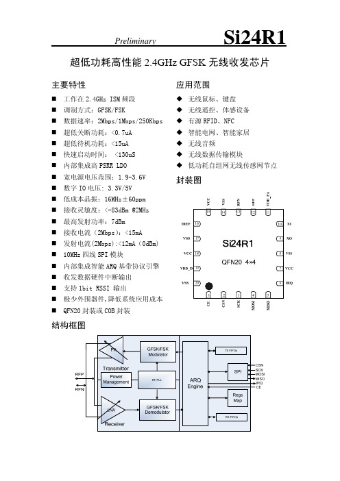
Si24R1
中文描述 自动重传请求 自动重发 自动重传延迟 误码率 芯片使能 循环冗余校验 片选 动态载波长度 高斯频移键控 中断请求 工业 科学 医学 最低有效位 兆位每秒 微控制器 兆赫兹 主机输入从机输出 主机输出从机输入 最高有效位 功率放大器 数据包识别位 载波 接收端 发射端 掉电 上电 射频通道 信号强度指示器 接收机 接收数据准备就绪 SPI 时钟 串行外设接口 发射机 已发数据 晶体振荡器
PrelimiLeabharlann arySi24R1目 录
1、简介.................................................. 4 2、引脚信息 .............................................. 5 3、工作模式 .............................................. 6 4、数据包处理协议 ........................................ 9 5、SPI数据与控制接口 .................................... 14 6、寄存器映射表 ......................................... 16 7、主要参数指标 ......................................... 22 8、封装................................................. 24 9、典型应用原理图 ....................................... 26 10、订单信息 ............................................ 29 附: 典型配置方案 ....................................... 30
LN2054_C南麟中文单片具有热调节功能的微型线性电池管理芯片充电管理丝印2YL6 2YL8
TJ=25℃,R =2K,IBAT=70mA PROG
5.0
5.5
6.0
6.5
7.0
Supply Voltage(V)
11. PROG 端上拉电流 VS 温度
PROG Pin Pull-up Current (uA)
8
7
6
5
4
3
2
1
0
-40
-20
VIN=6.5V, VBAT=4.3V, PROG=0V VIN=4.2V, VBAT=4.3V, PROG=0V
■ 用途
手机,PDA,MP3 蓝牙应用
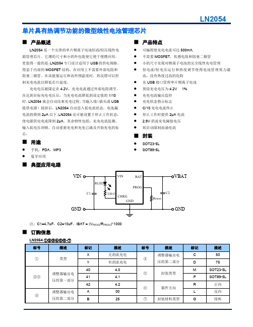
■ 典型应用电路
■ 产品特点
可编程使充电电流可达 500mA. 不需要 MOSFET,传感电阻和阻塞二极管 小的尺寸实现对锂离子电池的完全线性充电管理 恒电流/恒电压运行和热度调节使得电池管理效力最
高,没有热度过高的危险 从 USB 接口管理单片锂离子电池 预设充电电压为 4.2V 1% 充电电流输出监控 充电状态指示标志 C/10 充电电流终止 停止工作时提供 2µA 电流 2.9V 涓流充电阈值电压 软启动限制浪涌电流
20
单片具有热调节功能的微型线性电池管理芯片
LN2054
■ 产品概述
LN2054 是一个完善的单片锂离子电池恒流/恒压线性电 源管理芯片。它薄的尺寸和小的外包装使它便于便携应用。 更值得一提的是,LN2054 专门设计适用于 USB 的供电规格。 得益于内部的 MOSFET 结构,在应用上不需要外部电阻和 阻塞二极管。在高能量运行和高外围温度时,热反馈可以控 制充电电流以降低芯片温度。
Rprog=10k Rprog=2k Rprog=10k, Current mode Vchrg=5V Ichrg=5mA VFLOAT - VRECHRG
GT30L32S4W规格书V1.1I_A
● 数据总线: SPI 串行总线接口 ● 点阵排列方式:字节横置横排 访问速度:SPI 时钟频率: 80MHz(max.) ● 工作电压:2.7V~3.6V ● 电流:工作电流:20mA
待机电流:5uA ● 封装:SOP8-B ● 尺寸(SOP8-B):7.90mmX5.23mm ● 工作温度:-40℃~85℃ 存储温度:-55~125℃
5 引脚描述与接口连接 ......................................................................................................................................... 22
GT30L32S4W 标准汉字字库芯片规格书
GT30L32S4W
标准汉字字库芯片
规格书 DATASHEET
字符集:GB2312 字号:12x12、16x16、24x24、32x32 点阵 排置方式:横置横排 总线接口:SPI 串行总线 封装类型:SOP8-B
集通数码科技
V 1.0 I _A
2.1 指令参数 ........................................................................................................................................................................................12 2.2 Read Data Bytes(一般读取).......................................................................................................................................................12 2.3 Read Data Bytes at Higher Speed(快速读取点阵数据) ............................................................................................................13
BDR6122T-无线充电专用驱动芯片

1.60 0.90 0.30
Max. 0.80 0.05
0.30
1.65 0.95 0.35
V1.0
11
2017
8 PINS, SOP, 150MIL
BDR6122T
Symbol
A A1 A2 b c D E E1 e L
Notes: 1. Refer to JEDEC MS-012AA 2. All dimensions are in millimeter
V1.0
10
2017
封装资料
8-PIN, DFN
BDR6122T
Symbol
A A1 A3 b D E e D2 E2 L
Note: Refer to JEDEC MO-229
Min. 0.70
0
0.18
1.50 0.80 0.25
Dimensions Nom. 0.75 0.02
0.20 REF 0.25
V1.0
8
2017
典型工作特性
(如无特殊规定,VM=5V, VCC=3V)
BDR6122T
VM Sleep Current (nA)
12 10
8 6 4 2 0
-40 -20 0 20 40 60 80
Ambient Temperature (℃)
VCC Sleep Current (nA)
6 5 4 3 2 1 0
Power Supply
Motor Driver System
VM
Motor Driver
Local Bulk Capacitor
GND
IC Bypass Capacitor
RN8302B用户手册_v3.2介绍

深圳市锐能微科技有限公司
第2页
版本 3.1
3.4.5
3.4.17 3.3 和 3.4 章节
3.4.25 3.4.4 3.2.8
修订点
3.4.24 相电压电流状态寄存器
3.4.23.4.2 启动电流阈值寄存器
三相多功能防窃电计量芯片 RN8302B
注:
备注:高字节无效,读写按 3 字节操作。B1H~BBH 地址寄存器同 B0H 地址
三相多功能防窃电计量芯片 RN8302B
RN8302B 用户手册
日期:2011-6-20 初次发布
日期: 2013-8-16 升级至版本: 2.2 日期:2013-12-25 升级至 RN8302B(版本 v3.0) 日期:2014-7-15 升级至 RN8302B(版本 v3.1) 日期:2014-12-31 升级至 RN8302B(版本 v3.2)
修订点 1.4 典型应用
3.4.12 功率相位校正寄存器 5.5 SPI 读时序
修订点 1.3 管脚定义
修订点 在原 RN8302 基础上升级为
RN8302B
V2.1 修订说明
修订说明 图 1.3①将 U 通道电阻列分压电阻由 1MΩ改为 270KΩx8;② DVCC 上增加 10μF 和 0.1μF 电容,和表 1-1 管脚功能说明一 致。 改两处笔误,寄存器 B10H 改为 BAH,寄存器 B11H 改为 BBH 改一处笔误,RN8302B 收到读命令后,在 SCLK 的“上升沿” 将数据按位从 SDO 引脚输出。原为“下降沿”
深圳市锐能微科技有限公司
第1 页
版本 3.1
V2.0 修订说明
三相多功能防窃电计量芯片 RN8302B
修订点 基准电压
nRF24L01--中文资料
表 4 nRF24L01 电气特性
典型值
3.0 +27
16 160 320
1 2
0 18
1800
11.3 7.0 0.05 32 900
12.3 11.8 -82 -85
最大值
3.6 +85
VDD 0.3
单位 V
dBm kbps mA mA
dBm nA
COPYRIGHT ©2005 ALL RIGHTS RESERVED 迅通科技 TEL:+86 10 64390486 E-mail: sales@
分类信息
型号 nRF24L01 IC
nRF24L01 nRF24L01-EVKIT
nRF24L01 在不同模式下的引脚功能
引脚名称
方向
CE
输入
CSN
输入
SCK MOSI MISO IRQ
输入 输入 三态输出 输出
发送模式
接收模式
高电平>10us
高电平
SPI 片选使能 低电平使能
SPI 时钟 SPI 串行输入 SPI 串行输出 中断 低电平使能 表 7 nRF24L01 引脚功能
描述 确认信号 应答信号 自动重发 芯片使能 时钟信号 循环冗余校验 片选非 增强型 ShockBrustTM 高斯键控频移 中断请求 工业 科学 医学 低噪声放大 最低有效位 最低有效字节 兆位/秒 微控制器 主机输入从机输出 主机输出从机输入 最高有效位 最高有效字节 印刷电路板 数据包误码率 数据包识别位 载波 接收源 发射源 掉电 上电 接收 接收数据准备就绪 串行可编程接口 发送 已发送数据
亿佰特(Ebyte)-E01nRF24L01芯片-内置PA+LNA-带屏蔽-抗干扰-低辐射-板材特殊-耐高温的无线模块

E01 系列是成都公司标志性产品的 2.4G 无线模块,SPI 接口,目前已经稳定量产,并适用于多种应用场景。 E01 系列采用挪威 Nordic 公司原装进口的 nRF24L01P 芯片,所有阻容感器件均采用进口元器件,尤其是晶体,我们使用了高精度宽温晶体,保证其工业特 性。发射功率为 20dBm 的模块内置了 PA 功率放大器与 LNA 低噪声放大器,从而提高通信稳定性,延长通信距离;发射功率为 0dBm 的模块均采用进口器件, 优秀的设计亦保证了卓越的射频性能,是追求低功耗的客户首选。 E01 系列均严格遵守 FCC、CE、CCC 等国内国外设计规范,满足各项射频相关认证,满足出口要求。
1.1. 通用参数 3 1.2. 电气参数 3 1.2.1. 发射电流 3 1.2.2. 接收电流 3 1.2.3. 关断电流 3 1.2.4. 供电电压 4 1.2.5. 通信电平 4 1.3. 射频参数 4 1.3.1. 发射功率 4 1.3.2. 接收灵敏度 4 1.3.3. 推荐工作频率............................................................................................................................................................................................. 5 1.4. 实测参数 5 1.4.1. 实测距离 5 2. 机械特性.............................................................................................................................
无线充驱动芯片 BDR2L00

BDR2L00Half-Bridge DriverDESCRIPTIONThe BDR2L00 is a single Phase MOSFET gate driver optimized to drive the gates of both high-side and low-side power MOSFETs.FEATURES∙ Drive two N-MOSFETs∙ High-Frequency operation (Up to 1MHz) ∙ PWM input capable of 3.3V and 5V ∙ Fast output rise timeAPPLICATION CIRCUIT SOP8/DFN8:PIN CONFIGURATIONABSOLUTE MAXIMUM RATINGSStresses exceeding the absolute maximum ratings may damage the device or make the function abnormal. All the voltage parameters are absolute voltages referenced to IC PGND unless otherwise stated in the table.ELECTRICAL CHARACTERISTICSAPPLICATION INFORMATIONTheory of OperationThe BDR2L00 is an integrated driver and boot diode module designed for N+N half bridge driver. A single PWM input signal is all that is required to properly drive the high−side and low−side MOSFETs.Low−Side DriverThe low-side driver is designed to drive a ground−referenced low R DS(on)N−Channel MOSFET. The voltage rail for the low−side driver is internally connected to VCC and GND.High−Side DriverThe high-side driver is designed to drive a floating low RDS(ON) N−channel MOSFET. The gate voltage for the high side driver is developed by a bootstrap circuit referenced to Switch Node (PHASE) pin.The bootstrap circuit is comprised of the internal diode and an external bootstrap capacitor. When the BDR2L00 is starting up, the PHASE pin is at ground, so the bootstrap capacitor will charge up to VCC through the bootstrap diode. When the PWM input goes high, the high−side driver will begin to turn on the high−side MOSFET using the stored charge of the bootstrap capacitor. As the high−side MOSFET turns on, the PHASE pin will rise. When the high−side MOSFET is fully on, the switch node will be at 12V, and the BST pin will be at 5V plus the charge of the bootstrap capacitor (approaching 17V).The bootstrap capacitor is recharged when the switch node goes low during the next cycle.Safety Timer and Overlap Protection CircuitIt is very important that MOSFETs in a synchronous buck regulator do not both conduct at the same time. Excessive shoot−through or cross conduction can damage the MOSFETs, and even a small amount of cross conduction will cause a decrease in the power conversion efficiency.The BDR2L00 prevents cross conduction by monitoring the status of the MOSFETs and applying the appropriate amount of “dead−time” or the time between the turn off of one MOSFET and the turn on of the other MOSFET.When the PWM input pin goes high, the gate of the low−side MOSFET will go low after a propagation delay. The time it takes for the low−side MOSFET to turn off is dependent on the total charge on the low−side MOSFET gate. Likewise, when the PWM input pin goes low, the gate of the high−side MOSFET will go low after the propagation delay. The time to turn off the high−side MOSFET is dependent on the total gate charge of the high−side MOSFET.Enable (Only for DFN8)If EN pin is low level, whatever the PWM pin is high or low, all circuits are shutdown. If EN pin is high level, the outputs are controlled by PWM pin.Thermal ShutdownIf the driver temperature exceeds 170°C, the part will enter thermal shutdown and turn off both MOSFETs. Once the temperature falls below 150°C, the part will resume normal operation.Power Supply DecouplingThe BDR2L00 can source and sink relatively large current to the gate pins of the MOSFETs. In order to maintain a constant and stable supply voltage (VCC) a low ESR capacitor should be placed near the power and ground pins. A 2.2uF to 10uF multilayer ceramic capacitor (MLCC) is usually sufficient.Bootstrap CircuitThe bootstrap circuit uses a charge storage capacitor (C BST). The bootstrap capacitor must have a voltage rating that is able to withstand twice the maximum supply voltage. A minimum 16 V rating is recommended. A bootstrap capacitance greater than 680nF and a minimum 16V rating is recommended. A good quality ceramic capacitor should be used.PACKAGE INFORMATION 8 PINS, SOP, 150MIL8-PINS, DFN, 3X3。
- 1、下载文档前请自行甄别文档内容的完整性,平台不提供额外的编辑、内容补充、找答案等附加服务。
- 2、"仅部分预览"的文档,不可在线预览部分如存在完整性等问题,可反馈申请退款(可完整预览的文档不适用该条件!)。
- 3、如文档侵犯您的权益,请联系客服反馈,我们会尽快为您处理(人工客服工作时间:9:00-18:30)。
0.21
4.95 to 34
2
(40V Abs Max)
50 to 400 25
50 2A
12
1 to 3 Lithium
Adj. Timer
3x3 QFN-16
12
1 Nickle
Adj. Timer
2x2 DFN-6
12
1 Lithium
Thermal NTC 2x3 DFN-8
12
1 to 5 Lithium Adj. Timer or C/10 3x3 DFN-12
LTC4125: Monolithic 5W Wireless Power Transmitter
nn AutoResonant Switching Frequency Adjusts to Resonant Capacitance and Transmit Coil Inductance
nn Transmit Power Automatically Adjusts to Receiver Load nn Input Voltage Range: 3V to 5.5V nn Integrated 100mΩ Full Bridge Switches nn Multiple Foreign Object Detection Methods nn NTC Input for System/Component Temperature Qualified
Part Number Device Architecture Wireless Power Transmitter LTC4125 Wireless Transmitter
VIN Range (V)
Power Level AutoResonant Foreign Object
Optimum Practical Coupling Package
Power Transfer nn Thermally Enhanced 20-Lead 4mm × 5mm QFN Package
LTC4125 DC2386A/B Demo Kit Transmitter Demo Circuit
LTC4120 DC2386A/B Demo Kit Receiver/Charger Demo Circuit
Power Level Charge Practical Coupling
(W)
Current (mA) Distance (mm)
Cell(s) Chemistry
Charge Termination Package
Method
(mmxmm)
4.25 to 40
2
2.2 to 5
0.038
N/A Shunt
Lead-Acid
MSOP-12E
L, LT, LTC, LTM, Linear Technology and the Linear logo are registered trademarks and AutoResonant is a trademark of Linear Technology Corporation. All other trademarks are the property of their respective owners.
LTC4120 Product Page: /product/LTC4120 LTC4120 Application Note: /docs/43968
LTC4125 Product Page: /product/LTC4125 LTC4123 Product Page: /product/LTC4123
(W)
Drive
Detection
Power Transfer Distance (mm) (mmxmm)
3 to 5.5
5
Yes
Yes
Yes
13 Full Power 4x5 QFN-20
16 Half Power
Part Number Device Architecture
Battery Chargers
Wireless Power Transfer ICs
An inductive wireless power transfer (WPT) system consists of transmitter electronics, transmit coil, receive coil and receiver electronics. The LTC®4120-based resonant coupled system uses dynamic harmonization control (DHC) to optimize power transfer and provide overvoltage protection. This eliminates the need for precise mechanical alignment between the transmit and receive coils as well as the need for a coupling core. The LTC4120 wireless buck charger forms the basis for the receiver electronics. The receive coil can be integrated into the receiver electronics circuit board. The LTC4125 is a power controller for a simple but versatile wireless power transmitter. The LTC4125 enhances a basic wireless power transmitter by providing three additional key features: an AutoResonant™ function that maximizes available receiver power, an Optimum Power Search algorithm that maximizes overall wireless power system efficiency and foreign object detection to ensure safe and reliable operation when operating in the presence of conductive foreign objects.
COIL CENTER OFFSET (mm)
WIRELESS BATTERY CHARGING SYSTEM
Wireless Power Transfer System Charging Block Diagram
Battery Charge Power vs RX-TX Coil Location
Wireless Power Receiver and Buck Battery Charger
Wireless Power Receiver/Charger
The LTC4120, a high performance wireless receiver and battery charger, serves as the central component of the receiver electronics in a wireless battery charging system. The Linear Technology wireless power system is designed to transmit up to 2W to a battery with a maximum charge current of 400mA. The programmable float voltage of the device accommodates several battery chemistries and configurations. The IC utilizes a patented dynamic harmonization control (DHC) technique that enables high efficiency contactless charging with maximum TX to RX coil distance and misalignment without any of the thermal or overvoltage issues typically associated with wireless power systems. Wireless charging with the LTC4120 enables or improves many different applications. For instance, expensive connectors which become failure-prone in harsh environments can be eliminated. Similarly, wireless charging allows for a completely sealed enclosure for applications that require sterilization. Elimination of wires enables rechargeable batteries to be placed in moving or rotating equipment. Some applications are simply too small to use a conventional connector. Wireless charging can also provide transformerless galvanic isolation for high reliability isolated applications.