DW8522_Prelim_091113_Datasheet
Burster-Typ 8523 31-技术资料(德)

Anwendung Diese Typenreihen sind speziell zum Messen von statischen und quasistatischen Zug- oder Druckkräften geeignet. Die Membransensoren wurden nach bewährtem Prinzip konstruiert. Aufgrund ihrer Kompaktheit und der sehr soliden Ausführung sind sie sowohl für den Einsatz in Fertigungsanlagen als auch für Anwendungen im Labor und Prüffeld geeignet. Die Kennwerte der Sensoren (Ausnahme Typ 8523-20/50 N) sind standardisiert. Dadurch ist ein Austausch ohne Abgleich des Messverstärkers möglich. Außerdem können dadurch zur Summenbildung der Einzelkräfte Sensoren mit gleichem Messbereich parallel geschaltet werden.
1) Fehler aus Nichtlinearität, Umkehrspanne und Spannweite 2) Abweichungen vom angegebenen Wert sind möglich.
IR公司_大功率MOS管选型

I DContinuous Drain Current(A)70°Micro3Surface Mount PackagesV (BR)DSSDrain-to-Source Breakdown Voltage (V)R DS(on)On-State Resistance ()ΩI D Continuous Drain Current 25°C(A)R ΘMax.Thermal Resistance (°C/W)1FaxonDemand Number Case Outline KeyPartNumberPD Max.PowerDissipation (W)N-ChannelLogic LevelIRLML2402*912570.54200.25 1.20.95230H1IRLML2803912580.54300.251.20.93230P-ChannelLogic LevelIRLML6302*912590.54-200.6-0.62-4.8230H1IRLML5103912600.54-300.6-0.61-4.8230* Indicates low VGS(th), which can operate at VGS = 2.7VMeasured at ambient for Micro3, Micro6, Micro8, SO-8, and SOT-223 package styles. All others measured at case.1Micro3SO-8D-PakD -PakSOT-227Micro6SOT-223Micro82 Illustrations not to scaleI DContinuous Drain Current(A)70°Micro6Surface Mount PackagesV (BR)DSSDrain-to-Source Breakdown Voltage (V)R DS(on)On-State Resistance ()ΩI D Continuous Drain Current 25°C(A)R ΘMax.Thermal Resistance (°C/W)1FaxonDemand Number Case Outline KeyPartNumberPD Max.PowerDissipation (W)N-ChannelLogic LevelIRLMS1902915401.7200.10 3.2 2.675H2IRLMS1503915081.7300.103.22.675P-ChannelLogic LevelIRLMS6702*914141.7-200.20-2.3-1.975H2IRLMS5703914131.7-300.20-2.3-1.975* Indicates low VGS(th), which can operate at VGS = 2.7VMeasured at ambient for Micro3, Micro6, Micro8, SO-8, and SOT-223 package styles. All others measured at case.1Micro3SO-8D-PakD -PakSOT-227Micro6SOT-223Micro82 Illustrations not to scaleI DContinuous Drain Current(A)70°Micro8Surface Mount PackagesV (BR)DSSDrain-to-Source Breakdown Voltage (V)R DS(on)On-State Resistance ()ΩI D Continuous Drain Current 25°C(A)R ΘMax.Thermal Resistance (°C/W)1FaxonDemand Number Case Outline KeyPart NumberP D Max.PowerDissipation (W)N-Channel Logic LevelIRF7601* 912611.820 0.035 5.7 4.6 70 H3IRF7603 912621.830 0.035 5.6 4.5 70Dual N-Channel Logic LevelIRF7501* 912651.220 0.135 2.4 1.9 100 H3IRF7503 912661.2530 0.135 2.4 1.9 100P-Channel Logic LevelIRF7604* 912631.8-20 0.09 -3.6 -2.9 70 H3IRF7606 912641.8-30 0.09 -3.6 -2.9 70Dual P-Channel Logic LevelIRF7504* 912671.25-20 0.27 -1.7 -1.4 100 H3IRF7506 912681.25-30 0.27 -1.7 -1.4 100Dual N- and P-Channel Logic LevelIRF7507* 912691.2520 0.1352.4 1.9 100 H3-20 0.27 -1.7 -1.4IRF7509 912701.2530 0.135 2.4 1.9 100-30 0.27 -1.7 -1.4* Indicates low VGS(th), which can operate at VGS = 2.7VMeasured at ambient for Micro3, Micro6, Micro8, SO-8, and SOT-223 package styles. All others measured at case.1Micro3SO-8D-Pak D -PakSOT-227Micro6SOT-223Micro8 2 Illustrations not to scaleI DContinuous Drain Current(A)70°SO-8Surface Mount PackagesV (BR)DSSDrain-to-Source Breakdown Voltage (V)R DS(on)On-State Resistance ()ΩI D Continuous Drain Current 25°C(A)R ΘMax.Thermal Resistance (°C/W)1FaxonDemand Number Case Outline KeyPart Number P D Max.PowerDissipation (W)N-ChannelIRF7413913302.5300.011139.250H4IRF7413A 916132.5300.0135128.450IRF9410915622.5300.0375.850Dual N-ChannelIRF7311914352.0200.029 6.6 5.362.5H4IRF7313914802.0300.029 6.5 5.262.5IRF7333917002.0300.10 3.5 2.862.5917002.0300.050 4.9 3.962.5IRF9956915592.0300.103.52.862.5Dual P-ChannelIRF7314914352.0-200.058-5.3-4.362.5H4IRF7316915052.0-300.058-4.9-3.962.5IRF9953915602.0-300.25-2.3-1.862.5* Indicates low VGS(th), which can operate at VGS = 2.7VMeasured at ambient for Micro3, Micro6, Micro8, SO-8, and SOT-223 package styles. All others measured at case.1Micro3SO-8D-PakD -PakSOT-227Micro6SOT-223Micro82 Illustrations not to scaleI DContinuous Drain Current(A)70°SO-8Surface Mount PackagesV (BR)DSSDrain-to-Source Breakdown Voltage (V)R DS(on)On-State Resistance ()ΩI D Continuous Drain Current 25°C(A)RΘMax.ThermalResistance(°C/W)1FaxonDemand Number Case Outline KeyPart NumberP D Max.PowerDissipation (W)Dual N- and P-ChannelIRF7317 915682.020 0.029 6.6 5.3 62.5 H42.0-20 0.058 -5.3 -4.3 62.5IRF9952 915622.030 0.103.5 2.8 62.5915622.0-30 0.25 -2.3 -1.8 62.5IRF7319 916062.030 0.029 6.5 5.2 62.52.0-30 0.058 -4.9 -3.9 62.5* Indicates low VGS(th), which can operate at VGS = 2.7VMeasured at ambient for Micro3, Micro6, Micro8, SO-8, and SOT-223 package styles. All others measured at case.1Micro3SO-8D-Pak D -PakSOT-227Micro6SOT-223Micro8 2 Illustrations not to scaleI DContinuous Drain Current(A)70°SO-8Surface Mount PackagesV (BR)DSSDrain-to-Source Breakdown Voltage (V)R DS(on)On-State Resistance ()ΩI D Continuous Drain Current 25°C(A)R ΘMax.Thermal Resistance (°C/W)1FaxonDemand Number Case Outline KeyPart Number P D Max.PowerDissipation (W)N-ChannelLogic LevelIRF7401912442.5200.0228.77.050H4IRF7201911002.5300.0307.0 5.650IRF7403912452.5300.0228.55.450Dual N-ChannelLogic LevelIRF7101908712.0200.10 3.5 2.362.5H4IRF7301912382.0200.050 5.2 4.162.5IRF7303912392.0300.050 4.9 3.962.5IRF7103910952.0500.1303.02.362.5P-ChannelLogic LevelIRF7204911032.5-200.060-5.3-4.250H4IRF7404912462.5-200.040-6.7-5.450IRF7205911042.5-300.070-4.6-3.750IRF7406912472.5-300.045-5.8-3.750IRF7416913562.5-300.02-10-7.150* Indicates low VGS(th), which can operate at VGS = 2.7VMeasured at ambient for Micro3, Micro6, Micro8, SO-8, and SOT-223 package styles. All others measured at case.1Micro3SO-8D-PakD -PakSOT-227Micro6SOT-223Micro82 Illustrations not to scaleI DContinuous Drain Current(A)70°SO-8Surface Mount PackagesV (BR)DSSDrain-to-Source Breakdown Voltage (V)R DS(on)On-State Resistance ()ΩI D Continuous Drain Current 25°C(A)R ΘMax.Thermal Resistance (°C/W)1FaxonDemand Number Case Outline KeyPart Number P D Max.PowerDissipation (W)Dual P-ChannelLogic LevelIRF7104910962.0-200.250-2.3-1.862.5H4IRF7304912402.0-200.090-4.3-3.462.5IRF7306912412.0-300.10-3.6-2.962.5Dual N- and P-Channe Logic LevelIRF7307912421.4200.050 4.3 3.490H4-200.090-3.6-2.9IRF7105910972.0250.1093.5 2.862.52-250.25-2.3-1.862IRF7309912432.0300.050 4.9 3.962.5-300.10-3.6-2.9* Indicates low VGS(th), which can operate at VGS = 2.7VMeasured at ambient for Micro3, Micro6, Micro8, SO-8, and SOT-223 package styles. All others measured at case.1Micro3SO-8D-PakD -PakSOT-227Micro6SOT-223Micro82 Illustrations not to scaleI DContinuous Drain Current(A)70°SOT-223Surface Mount PackagesV (BR)DSSDrain-to-Source Breakdown Voltage (V)R DS(on)On-State Resistance ()ΩI D Continuous Drain Current 25°C(A)R ΘMax.Thermal Resistance (°C/W)1FaxonDemand Number Case Outline KeyPart Number P D Max.PowerDissipation (W)N-ChannelIRFL4105913812.1550.045 3.7 3.060H6IRFL110908612.01000.54 1.50.9660IRFL4310913682.11000.20 1.6 1.360IRFL21090868 2.02001.50.960.660IRFL214908622.02502.00.790.560P-ChannelIRFL9110908642.0-1001.2-1.1-0.6960H6N-ChannelLogic LevelIRLL3303913792.1300.031 4.6 3.760H6IRLL014N 914992.1550.14 2.0 1.660IRLL2705913802.1550.043.83.060* Indicates low VGS(th), which can operate at VGS = 2.7VMeasured at ambient for Micro3, Micro6, Micro8, SO-8, and SOT-223 package styles. All others measured at case.1Micro3SO-8D-PakD -PakSOT-227Micro6SOT-223Micro82 Illustrations not to scaleI DContinuous Drain Current(A)100°D-PakSurface Mount PackagesV (BR)DSSDrain-to-Source Breakdown Voltage (V)R DS(on)On-State Resistance ()ΩI D Continuous Drain Current 25°C(A)R ΘMax.Thermal Resistance (°C/W)1FaxonDemand Number Case Outline KeyPart Number P D Max.PowerDissipation (W)N-ChannelIRFR33039164257300.0313321 2.2H7IRFR024N9133638550.0751610 3.3IRFR41059130248550.0452516 2.7IRFR12059131869550.0273723 1.8IRFR11090524251000.54 4.3 2.75IRFR120N 91365391000.219.1 5.8 3.2IRFR391091364521000.11159.5 2.4IRFR2109052625200 1.5 2.6 1.75IRFR22090525422000.8 4.833IRFR21490703252502 2.2 1.45IRFR2249060042250 1.1 3.8 2.43IRFR3109059725400 3.6 1.7 1.15IRFR3209059842400 1.8 3.123IRFR42090599425003 2.4 1.53IRFRC2090637426004.421.33* Indicates low VGS(th), which can operate at VGS = 2.7VMeasured at ambient for Micro3, Micro6, Micro8, SO-8, and SOT-223 package styles. All others measured at case.1Micro3SO-8D-PakD -PakSOT-227Micro6SOT-223Micro82 Illustrations not to scaleI DContinuous Drain Current(A)100°D-PakSurface Mount PackagesV (BR)DSSDrain-to-Source Breakdown Voltage (V)R DS(on)On-State Resistance ()ΩI D Continuous Drain Current 25°C(A)R ΘMax.Thermal Resistance (°C/W)1FaxonDemand Number Case Outline KeyPart Number P D Max.PowerDissipation (W)P-ChannelIRFR55059161057-550.11-18-11 2.2H7IRFR53059140289-550.065-28-18 1.4IRFR90149065425-600.5-5.1-3.25IRFR90249065542-600.28-8.8-5.63IRFR91109051925-100 1.2-3.1-25IRFR91209052042-1000.6-5.6-3.63IRFR9120N 9150739-1000.48-6.5-4.1 3.2IRFR92109052125-2003-1.9-1.25IRFR92209052242-200 1.5-3.6-2.33IRFR92149165850-250 3.0-2.7-1.7 2.5IRFR93109166350-4007.0-1.8-1.12.5* Indicates low VGS(th), which can operate at VGS = 2.7VMeasured at ambient for Micro3, Micro6, Micro8, SO-8, and SOT-223 package styles. All others measured at case.1Micro3SO-8D-PakD -PakSOT-227Micro6SOT-223Micro82 Illustrations not to scaleI DContinuous Drain Current(A)100°D-PakSurface Mount PackagesV (BR)DSSDrain-to-Source Breakdown Voltage (V)R DS(on)On-State Resistance ()ΩI D Continuous Drain Current 25°C(A)R ΘMax.Thermal Resistance (°C/W)1FaxonDemand Number Case Outline KeyPart Number P D Max.PowerDissipation (W)N-ChannelLogic LevelIRLR27039133538300.0452214 3.3H7IRLR33039131657300.0313321 2.2IRLR31039133369300.0194629 1.8IRLR024N 9136338550.0651711 3.3IRLR27059131746550.042415 2.7IRLR29059133469550.0273623 1.8IRLR120N 91541391000.18511 6.9 3.2IRLR341091607521000.10159.52.4* Indicates low VGS(th), which can operate at VGS = 2.7VMeasured at ambient for Micro3, Micro6, Micro8, SO-8, and SOT-223 package styles. All others measured at case.1Micro3SO-8D-PakD -PakSOT-227Micro6SOT-223Micro82 Illustrations not to scaleI DContinuous Drain Current(A)100°D 2PakSurface Mount PackagesV (BR)DSSDrain-to-Source Breakdown Voltage (V)R DS(on)On-State Resistance ()ΩI D Continuous Drain Current 25°C(A)R ΘMax.Thermal Resistance (°C/W)1FaxonDemand Number Case Outline KeyPart NumberP D Max.PowerDissipation (W)N-ChannelIRFZ24NS 913554555 0.07 17 12 3.3 H10IRFZ34NS 913116855 0.04 29 20 2.2IRFZ44NS 9131511055 0.022 49 35 1.4IRFZ46NS 9130512055 0.020 53 37 1.3IRFZ48NS 9140814055 0.016 64 45 1.1IRF1010NS 913723.855 0.011 84 60 40IRF3205S 9130420055 0.008 110 80 0.75IRFZ44ES 9171411060 0.023 48 34 1.4IRF1010ES 9172017060 0.012 83 59 0.90IRF2807S 9151815075 0.013 71 50 1.0IRF520NS 9134047100 0.2 9.5 6.7 3.2IRF530NS 9135263100 0.11 15 11 2.4IRF540NS 91342110100 0.052 27 19 1.6IRF1310NS 91514120100 0.036 36 25 1.3IRF3710S 91310150100 0.028 46 33 1.0IRF3315S 9161794150 0.082 21 15 1.6IRF3415S 91509150150 0.042 37 26 1.0IRFBC20S 9.101450600 4.4 2.2 1.4 2.5IRFBC30S 9101574600 2.2 3.6 2.3 1.7IRFBC40S 91016130600 1.2 6.2 3.9 1.0* Indicates low VGS(th), which can operate at VGS = 2.7VMeasured at ambient for Micro3, Micro6, Micro8, SO-8, and SOT-223 package styles. All others measured at case.1Micro3SO-8D-Pak D -PakSOT-227Micro6SOT-223Micro8 2 Illustrations not to scaleI DContinuous Drain Current(A)100°D 2PakSurface Mount PackagesV (BR)DSSDrain-to-Source Breakdown Voltage (V)R DS(on)On-State Resistance ()ΩI D Continuous Drain Current 25°C(A)R ΘMax.Thermal Resistance (°C/W)1FaxonDemandNumberCase Outline KeyPart NumberP D Max.PowerDissipation (W)IRFBF20S 9166554900 8.0 1.7 1.1 2.3 H10P-ChannelIRF5305S 91386110-55 0.06 -31 -22 1.4 H10IRF4905S 914783.8-55 0.02 -74 -52 40IRF9520NS 9152247-100 0.48 -6.7 -4.8 3.2IRF9530NS 9152375-100 0.20 -14 -9.9 2.0IRF9540NS 9148394-100 0.117 -19 -13 1.6IRF5210S 91405150-100 0.06 -35 -25 1.0* Indicates low VGS(th), which can operate at VGS = 2.7VMeasured at ambient for Micro3, Micro6, Micro8, SO-8, and SOT-223 package styles. All others measured at case.1Micro3SO-8D-Pak D -PakSOT-227Micro6SOT-223Micro8 2 Illustrations not to scaleI DContinuous Drain Current(A)100°D 2PakSurface Mount PackagesV (BR)DSSDrain-to-Source Breakdown Voltage (V)R DS(on)On-State Resistance ()ΩI D Continuous Drain Current 25°C(A)R ΘMax.Thermal Resistance (°C/W)1FaxonDemand Number Case Outline KeyPart NumberP D Max.PowerDissipation (W)N-Channel Logic LevelIRL3302S 916925720 0.020 39 25 2.2 H10IRL3202S916756920 0.016 48 30 1.8IRL3102S 916918920 0.013 61 39 1.4IRL3402S 9169311020 0.01 85 54 1.1IRL3502S 9167614020 0.007 110 67 0.89IRL2703S 913604530 0.04 24 17 3.3IRL3303S 913236830 0.026 38 27 2.2IRL3103S 9133811030 0.014 64 45 1.4IRL2203NS 9136717030 0.007 116 82 0.90IRL3803S 9131920030 0.006 140 98 0.75IRLZ24NS 913584555 0.06 18 13 3.3IRLZ34NS 913086855 0.035 30 21 2.2IRLZ44NS 9134711055 0.022 47 33 1.4IRL3705NS 9150217055 0.01 89 63 0.90IRL2505S 9132620055 0.008 104 74 0.75IRLZ44S 9090615060 0.028 50 36 1.0IRL530NS 9134963100 0.1 15 11 2.4IRL2910S 91376150100 0.026 48 34 1.0* Indicates low VGS(th), which can operate at VGS = 2.7VMeasured at ambient for Micro3, Micro6, Micro8, SO-8, and SOT-223 package styles. All others measured at case.1Micro3SO-8D-Pak D -PakSOT-227Micro6SOT-223Micro8 2 Illustrations not to scaleI DContinuous Drain Current(A)100°SOT-227Surface Mount PackagesV (BR)DSSDrain-to-Source Breakdown Voltage (V)R DS(on)On-State Resistance ()ΩI D Continuous DrainCurrent 25°C(A)RΘMax.Thermal Resistance (°C/W)1FaxonDemand Number Case Outline KeyPart Number P D Max.PowerDissipation (W)N-ChannelFully Isolated Low ChargeFA38SA50LC 916155005000.1338240.25H21FA57SA50LC916506255000.0857360.20* Indicates low VGS(th), which can operate at VGS = 2.7VMeasured at ambient for Micro3, Micro6, Micro8, SO-8, and SOT-223 package styles. All others measured at case.1Micro3SO-8D-PakD -PakSOT-227Micro6SOT-223Micro82 Illustrations not to scaleI DContinuous Drain Current(A)100°I-PakThrough-Hole PackagesV (BR)DSSDrain-to-Source Breakdown Voltage (V)R DS(on)On-State Resistance ()ΩI D Continuous Drain Current 25°C(A)R ΘMax.Thermal Resistance (°C/W)1FaxonDemand Number Case Outline KeyPart Number P D Max.PowerDissipation (W)N-ChannelIRFU33039164257300.0313321 2.2H8IRFU024N 9133638550.0751610 3.3IRFU41059130248550.0452519 2.7IRFU12059131869550.0273723 1.8IRFU11090524251000.54 4.3 2.7 5.0IRFU120N 91365391000.219.1 5.8 3.2IRFU391091364521000.11159.5 2.4IRFU2109052625200 1.5 2.6 1.7 5.0IRFU22090525422000.80 4.8 3.0 3.0IRFU2149070325250 2.0 2.2 1.4 5.0IRFU2249060042250 1.1 3.8 2.4 3.0IRFU3109059725400 3.6 1.7 1.1 5.0IRFU3209059842400 1.8 3.1 2.0 3.0IRFU4209059942500 3.0 2.4 1.5 3.0IRFUC2090637426004.42.01.33.0I-PakTO-220 FullPakTO-262TO-247HEXDIPTO-220AB Illustrations not to scale** Not ratedI DContinuous Drain Current(A)100°I-PakThrough-Hole PackagesV (BR)DSSDrain-to-Source Breakdown Voltage (V)R DS(on)On-State Resistance ()ΩI D Continuous Drain Current 25°C(A)R ΘMax.Thermal Resistance (°C/W)1FaxonDemand Number Case Outline KeyPart Number P D Max.PowerDissipation (W)P-ChannelIRFU55059161057-550.11-18-11 2.2H8IRFU53059140289-550.065-28-18 1.4IRFU90149065425-600.50-5.1-3.2 5.0IRFU90249065542-600.28-8.8-5.6 3.0IRFU91109051925-100 1.2-3.1-2.0 5.0IRFU91209052042-1000.60-5.6-3.6 3.0IRFU9120N 9150739-1000.48-6.5-4.1 3.2IRFU92109052125-200 3.0-1.9-1.2 5.0IRFU92209052242-200 1.5-3.6-2.3 3.0IRFU92149165850-2503.0-2.7-1.7 2.5IRFU93109166350-4007.0-1.8-1.12.5N-ChannelLogic LevelIRLU27039133538300.0452214 3.3H8IRLU33039131657300.0313321 2.2IRLU31039133369300.0194629 1.8IRLU024N 9136338550.0651711 3.3IRLU27059131746550.04241715IRLU29059133469550.0273623 1.8IRLU120N 91541391000.18511 6.9 3.2IRLU341091607521000.10159.52.4I-PakTO-220 FullPakTO-262TO-247HEXDIPTO-220AB Illustrations not to scale** Not ratedI DContinuous Drain Current(A)100°HEXDIPThrough-Hole PackagesV (BR)DSSDrain-to-Source Breakdown Voltage (V)R DS(on)On-State Resistance ()ΩI D Continuous Drain Current 25°C(A)R ΘMax.Thermal Resistance (°C/W)1FaxonDemand Number Case Outline KeyPart Number P D Max.PowerDissipation (W)N-ChannelIRFD014907001.3600.2 1.7 1.2120H9IRFD024906991.3600.1 2.5 1.8120IRFD110903281.31000.54 1.00.71120IRFD120903851.31000.27 1.30.94120IRFD210903861.3200 1.50.60.38120IRFD220904171.32000.80.80.50120IRFD214912711.3250 2.00.570.32120IRFD224912721.3250 1.10.760.43120IRFD310912251.3400 3.60.420.23120IRFD320912261.3400 1.80.600.33120IRFD420912271.3500 3.00.460.26120IRFDC20912281.36004.40.320.21120I-PakTO-220 FullPakTO-262TO-247HEXDIPTO-220AB Illustrations not to scale** Not ratedI D Continuous Drain Current (A)100°TO-220Qg TotalGate Charge(nC)Through-Hole PackagesV (BR)DSSDrain-to-Source Breakdown Voltage (V)R DS(on)On-State Resistance ()ΩI D Continuous Drain Current 25°C (A)R ΘMax.Thermal Resistance(°C/W)1Faxon Demand Number Case OutlineKeyPart Number P D Max.Power Dissipation (W)N-ChannelLow ChargeIRF737LC91314743000.75 6.1** 1.7 3.9H11IRF740LC 910681254000.5510** 1.039IRF840LC 910691255000.858.0** 1.039IRFBC40LC910701256001.26.2**1.039I-PakTO-220 FullPakTO-262TO-247HEXDIPTO-220AB Illustrations not to scale** Not ratedI DContinuous Drain Current(A)100°TO-220ABThrough-Hole PackagesV (BR)DSSDrain-to-Source Breakdown Voltage (V)R DS(on)On-State Resistance ()ΩI D Continuous Drain Current 25°C(A)R ΘMax.Thermal Resistance (°C/W)1FaxonDemand Number Case Outline KeyPart Number P D Max.PowerDissipation (W)N-ChannelIRFZ24N 9135445550.071712 3.3H12IRFZ34N9127656550.042618 2.7IRFZ44N 9130383550.0244129 1.8IRFZ46N 9127788550.024633 1.7IRFZ48N 9140694550.0165337 1.6IRF1010N 91278130550.0127251 1.2IRF320591279150550.0089869 1.0IRFZ34E 9167268600.0422820 2.2IRFZ44E 91671110600.0234834 1.4IRF1010E 91670170600.01281570.90IRF280791517150750.0137150 1.0IRF520N 91339471000.209.5 6.79.5IRF530N 91351601000.111511 2.4IRF540N 91341941000.0522719 1.6IRF1310N 916111201000.0363625 1.3IRF3710913091501000.0284633 1.0IRF331591623941500.0822115 1.6IRF3415914771501500.0423726 1.0IRFBC209062350600 4.4 2.2 1.4 2.5IRFBC309048274600 2.2 3.6 2.3 1.7IRFBC4090506125600 1.2 6.2 3.9 1.0IRFBE2090610548006.51.81.22.3I-PakTO-220 FullPakTO-262TO-247HEXDIPTO-220AB Illustrations not to scale** Not ratedI DContinuous Drain Current(A)100°TO-220ABThrough-Hole PackagesV (BR)DSSDrain-to-Source Breakdown Voltage (V)R DS(on)On-State Resistance ()ΩI D Continuous Drain Current 25°C(A)R ΘMax.Thermal Resistance (°C/W)1FaxonDemand Number Case Outline KeyPart Number P D Max.PowerDissipation (W)IRFBE3090613125800 3.0 4.1 2.6 2.0H12IRFBF3090616125900 3.7 3.6 2.3 1.0IRFBG209060454100011 1.40.86 2.3IRFBG309062012510005.03.12.01.0P-ChannelIRF9Z24N 9148445-550.175-12-8.53.3H12IRF9Z34N 9148556-550.10-17-12 2.7IRF530591385110-550.06-31-22 1.4IRF490591280150-550.02-64-45 1.0IRF9530N 9148275-1000.20-13-9.2 2.0IRF9540N 9143794-1000.117-19-13 1.6IRF521091434150-1000.06-35-25 1.0IRF62159147983-1500.29-11-7.81.8I-PakTO-220 FullPakTO-262TO-247HEXDIPTO-220AB Illustrations not to scale** Not ratedI DContinuous Drain Current(A)100°TO-220ABThrough-Hole PackagesV (BR)DSSDrain-to-Source Breakdown Voltage (V)R DS(on)On-State Resistance ()ΩI D Continuous Drain Current 25°C(A)R ΘMax.Thermal Resistance (°C/W)1FaxonDemand Number Case Outline KeyPart NumberP D Max.PowerDissipation (W)N-Channel Logic LevelIRL3302 916965720 0.020 39 25 2.2 H12IRL3202 916956920 0.016 48 30 1.8IRL3102 916948920 0.013 61 39 1.4IRL3402 9169711020 0.01 85 54 1.1IRL3502 9169814020 0.007 110 67 0.89IRL2703 913594530 0.04 24 17 3.3IRL3303 913225630 0.026 34 24 2.7IRL3103 913378330 0.014 56 40 1.8IRL2203N 9136613030 0.007 100 71 1.230 0.007 61 43 3.2IRL3803 9130115030 0.006 120 83 1.0IRLZ24N 913574555 0.06 18 13 3.3IRLZ34N 913075655 0.035 27 19 2.7IRLZ44N 913468355 0.022 41 29 1.8IRL3705N 9137013055 0.01 77 54 1.2IRL2505 9132520055 0.008 104 74 0.75IRL520N 9149447100 0.18 10 7.1 3.2IRL530N 9134863100 0.10 15 11 2.4IRL540N 9149594100 0.044 30 21 1.6IRL2910 91375150100 0.026 48 34 1.0I-PakTO-220 FullPakTO-262TO-247HEXDIPTO-220AB Illustrations not to scale** Not ratedI D Continuous Drain Current (A)100°TO-220 FullPak (Fully Isolated)Qg TotalGate Charge(nC)Through-Hole PackagesV (BR)DSSDrain-to-Source Breakdown Voltage (V)R DS(on)On-State Resistance ()ΩI D Continuous DrainCurrent 25°C(A)R ΘMax.Thermal Resistance (°C/W)1Fax on Demand Number Case OutlineKeyPart Number P D Max.Power Dissipation (W)N-ChannelLow ChargeIRFI740GLC91209404000.55 6.0** 3.139H13IRFI840GLC 91208405000.85 4.8** 3.139IRFIBC40GLC91211406001.24.0**3.139I-PakTO-220 FullPakTO-262TO-247HEXDIPTO-220AB Illustrations not to scale** Not ratedI DContinuous Drain Current(A)100°TO-220 FullPak (Fully Isolated)Through-Hole PackagesV (BR)DSSDrain-to-Source Breakdown Voltage (V)R DS(on)On-State Resistance ()ΩI D Continuous Drain Current 25°C(A)R ΘMax.Thermal Resistance (°C/W)1FaxonDemand Number Case Outline KeyPart Number P D Max.PowerDissipation (W)N-ChannelIRFIZ24N 9150126550.07139.2 5.8H14IRFIZ34N9148931550.041913 4.8IRFIZ44N 9140338550.02428200.024IRFIZ46N 9130640550.023122 3.8IRFIZ48N 9140742550.0163625 3.6IRFI1010N 9137347550.0124431 3.2IRFI32059137448550.0085640 3.1IRFIZ24E 9167329600.071149.6 5.2IRFIZ34E 9167437600.0422115 4.1IRFI510G 90829271000.54 4.5 3.2 5.5IRFI520N 91362271000.207.2 5.1 5.5IRFI530N 91353331000.11117.8 4.5IRFI540N 91361421000.0521813 3.6IRFI1310N 91611451000.0362216 3.3IRFI371091387481000.0252820 3.1IRFI620G 90832302000.8 4.1 2.6 4.1IRFI630G 90652322000.4 5.9 3.7 3.6IRFI640G 90649402000.189.8 6.2 3.1IRFI614G 9083123250 2.0 2.1 1.3 5.5IRFI624G 9083330250 1.1 3.4 2.2 4.1IRFI634G 90738322500.45 5.6 3.5 3.6IRFI644G 90739402500.287.953.1I-PakTO-220 FullPakTO-262TO-247HEXDIPTO-220AB Illustrations not to scale** Not ratedI DContinuous Drain Current(A)100°TO-220 FullPak (Fully Isolated)Through-Hole PackagesV (BR)DSSDrain-to-Source Breakdown Voltage (V)R DS(on)On-State Resistance ()ΩI D Continuous Drain Current 25°C(A)R ΘMax.Thermal Resistance (°C/W)1FaxonDemand Number Case Outline KeyPart Number P D Max.PowerDissipation (W)IRFI720G 9083430400 1.8 2.6 1.7 4.1H14IRFI730G 9065032400 1.0 3.7 2.3 3.6IRFI740G 90651404000.55 5.4 3.4 3.1IRFI734G 9100135450 1.2 3.4 2.1 3.6IRFI744G 91002404500.63 4.9 3.1 3.1IRFI820G 9064130500 3.0 2.1 1.3 4.1IRFI830G 9064632500 1.5 3.12 3.6IRFI840G 90642405000.85 4.6 2.9 3.1IRFIBC20G 90850306004.41.71.1 4.1IRFIBC30G 90851356002.2 2.5 1.63.6IRFIBC40G 9085240600 1.2 3.5 2.2 3.1IRFIBE20G 9085330800 6.5 1.4.86 4.1IRFIBE30G 9085435800 3.0 2.1 1.4 3.6IRFIBF20G 90855309008.0 1.2.79 4.1IRFIBF30G90856359003.71.91.23.6P-ChannelIRFI9Z24N 9152929-550.175-9.5-6.7 5.2H14IRFI9Z34N 9153037-550.10-14-10 4.1IRFI49059152663-550.02-41-29 2.4IRFI9540G 9083742-1000.117-13-9.2 3.6IRFI9540N 9148742-1000.117-13-9.2 3.6IRFI52109140448-1000.06-20-14 3.1IRFI9634G 9148835-2501.0-4.1-2.63.6I-PakTO-220 FullPakTO-262TO-247HEXDIPTO-220AB Illustrations not to scale** Not ratedI DContinuous Drain Current(A)100°TO-220 FullPak (Fully Isolated)Through-Hole PackagesV (BR)DSSDrain-to-Source Breakdown Voltage (V)R DS(on)On-State Resistance ()ΩI D Continuous Drain Current 25°C(A)R ΘMax.Thermal Resistance (°C/W)1FaxonDemand Number Case Outline KeyPart Number P D Max.PowerDissipation (W)N-ChannelLogic LevelIRLI2203N 9137847300.0076143 3.2H14IRLI38039132048300.0066747 3.1IRLIZ24N 9134426550.06149.9 5.8IRLIZ34N 9132931550.0352014 4.8IRLIZ44N 9149838550.0222820 4.0IRLI3705N 9136947550.014733 3.2IRLI25059132763550.00858412.4IRLI520N 91496271000.187.7 5.4 5.5IRLI530N 91350331000.10117.8 4.5IRLI540N 91497421000.04420143.6IRLI291091384481000.02627193.1P-ChannelLogic LevelIRFI9520G 9083537-1000.6-5.2-3.6 4.1H14IRFI9530G 9083638-1000.03-7.7-5.4 3.6IRFI9620G 9087430-200 1.5-3.0-1.9 4.1IRFI9630G 9083840-2000.8-4.3-2.7 3.6IRFI9640G9083940-2000.5-6.1-3.93.1I-PakTO-220 FullPakTO-262TO-247HEXDIPTO-220AB Illustrations not to scale** Not ratedI D Continuous Drain Current (A)100°TO-247Qg TotalGate Charge(nC)Through-Hole PackagesV (BR)DSSDrain-to-Source Breakdown Voltage (V)R DS(on)On-State Resistance ()ΩI D Continuous Drain Current 25°C (A)R ΘMax.Thermal Resistance (°C/W)1Fax on Demand Number Case OutlineKeyPart Number P D Max.Power Dissipation (W)1N-ChannelLow ChargeIRFP350LC912291904000.3018**0.6570H16IRFP360LC 912302804000.2023**0.4598IRFP450LC 912311905000.4016**0.6570IRFP460LC 912322805000.2720**0.4598IRFPC50LC 912331906000.6013**0.6570IRFPC60LC912342806000.4016**0.4598I-PakTO-220 FullPakTO-262TO-247HEXDIPTO-220AB Illustrations not to scale** Not rated。
8521码型
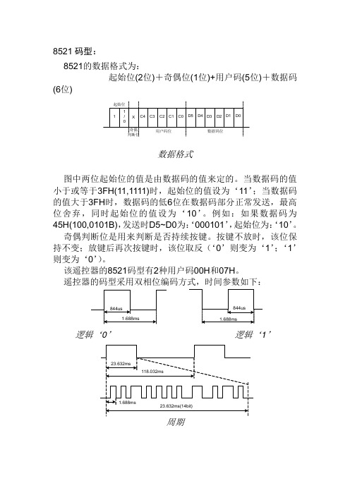
8521码型:8521的数据格式为:起始位(2位)+奇偶位(1位)+用户码(5位)+数据码(6位)数据格式图中两位起始位的值是由数据码的值来定的。
当数据码的值小于或等于3FH(11,1111)时,起始位的值设为‘11’;当数据码的值大于3FH 时,数据码的低6位在数据码部分正常发送,最高位舍弃,同时起始位的值设为‘10’。
例如:如果数据码为45H(100,0101B),发送时D5~D0为:‘000101’,起始位为:‘10’。
奇偶判断位是用来判断是否持续按键。
按键不放时,该位保持不变;放键后再次按键时,该位取反(‘0’则变为‘1’;‘1’则变为‘0’)。
该遥控器的8521码型有2种用户码00H 和07H 。
遥控器的码型采用双相位编码方式,时间参数如下:逻辑‘0’ 逻辑‘1’周期载波脉冲载波频率=1/12fosc=38KHzUPD6122码型:UPD6122的一帧数据中包含引导码,8位用户编码(C0~C7), 8位用户编码’(C0’~C7’) 8位键数据编码(D0~D7)以及8位键数据编码反码。
其数据格式如下图所示:(8位)(8位)(8位)(8位)如上图所示:第一帧完整的发射码由引导码、用户编码和键数据码三部分组成。
引导码由一个9ms 高电平脉冲及4.5ms 的低电平脉冲组成;十六位用户编码只发送一次;八位的键数据码连续发送两次,第一次发送的是原码,第二次发送的是反码。
第二帧开始只发一个由9ms 高电平脉冲、2.25ms 的低电平脉冲及560us 高电平脉冲的尾码。
本电路中的6122码型有2种不同的用户码:50AFH (0000 1010 1111 0101), 00FDH (0000 0000 1011 1111)。
6122编码采用脉冲位置调制方式(PPM ),根据低电平时间的长度判断“0”码和“1”码。
输出波形时间参数如下图所示:遥控器的发码规则:载波脉冲载波频率=38KHz2、3010码型:3010的数据格式为:起始位(2位)+奇偶位(1位)+用户码(5位)+数据码(6位)数据格式图中两位起始位的值是由数据码的值来定的。
Richtek技术有限公司RT8525GS产品说明书
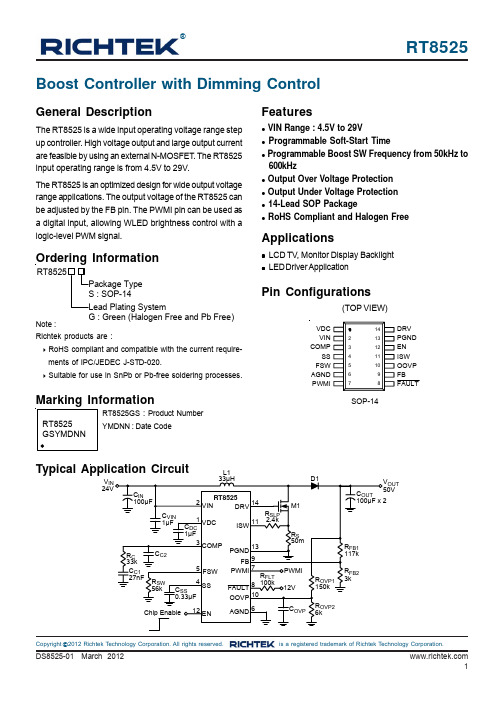
RT8525®DS8525-01 March 20121©Copyright 2012 Richtek Technology Corporation. All rights reserved. is a registered trademark of Richtek Technology Corporation.Ordering InformationNote :Richtek products are :` RoHS compliant and compatible with the current require-ments of IPC/JEDEC J-STD-020.` Suitable for use in SnPb or Pb-free soldering processes.Boost Controller with Dimming ControlPin ConfigurationsSOP-14(TOP VIEW)RT8525GS : Product NumberYMDNN : Date CodeGeneral DescriptionThe RT8525 is a wide input operating voltage range step up controller. High voltage output and large output current are feasible by using an external N-MOSFET . The RT8525input operating range is from 4.5V to 29V.The RT8525 is an optimized design for wide output voltage range applications. The output voltage of the RT8525 can be adjusted by the FB pin. The PWMI pin can be used as a digital input, allowing WLED brightness control with a logic-level PWM signal.FeatureszVIN Range : 4.5V to 29VzProgrammable Soft-Start Timez Programmable Boost SW Frequency from 50kHz to 600kHzz Output Over Voltage Protection z Output Under Voltage Protection z 14-Lead SOP Packagez RoHS Compliant and Halogen FreeApplicationszLCD TV, Monitor Display Backlight zLED Driver ApplicationDRV PGND ISW EN OOVP FB FAULTVDC VIN COMPSS FSW AGND PWMITypical Application CircuitG : Green (Halogen Free and Pb Free)L1V OUT2RT8525DS8525-01 March 2012©Copyright 2012 Richtek Technology Corporation. All rights reserved. is a registered trademark of Richtek Technology Corporation.Function Block Diagram3RT8525DS8525-01 March 2012©Copyright 2012 Richtek Technology Corporation. All rights reserved. is a registered trademark of Richtek Technology Corporation.Electrical Characteristics(V IN = 21V, V OUT = 50V, T A = 25°C, unless otherwise specified)Absolute Maximum Ratings (Note 1)z VIN to GND ------------------------------------------------------------------------------------------------------------------ −0.3V to 32V z VDC, DRV, FAULT to GND----------------------------------------------------------------------------------------------- −0.3V to 13.2V z EN, COMP , SS, FSW, FB, OOVP , ISW, PWMI to GND --------------------------------------------------------- −0.3V to 6V zPower Dissipation, P D @ T A = 25°CSOP-14----------------------------------------------------------------------------------------------------------------------1.000W zPackage Thermal Resistance (Note 2)SOP-14 , θJA ----------------------------------------------------------------------------------------------------------------100°C/W z Lead Temperature (Soldering, 10 sec.)-------------------------------------------------------------------------------260°C z Junction T emperature -----------------------------------------------------------------------------------------------------150°Cz Storage T emperature Range -------------------------------------------------------------------------------------------- −65°C to 150°C zESD Susceptibility (Note 3)HBM --------------------------------------------------------------------------------------------------------------------------2kV MM ----------------------------------------------------------------------------------------------------------------------------200VRecommended Operating Conditions (Note 4)z Supply Input Voltage, VIN -----------------------------------------------------------------------------------------------4.5V to 29V z Junction T emperature Range -------------------------------------------------------------------------------------------- −40°C to 125°C zAmbient T emperature Range -------------------------------------------------------------------------------------------- −40°C to 85°C4RT8525DS8525-01 March 2012©Copyright 2012 Richtek Technology Corporation. All rights reserved. is a registered trademark of Richtek Technology Corporation.Note 1. Stresses beyond those listed “Absolute Maximum Ratings ” may cause permanent damage to the device. These arestress ratings only, and functional operation of the device at these or any other conditions beyond those indicated in the operational sections of the specifications is not implied. Exposure to absolute maximum rating conditions may affect device reliability.Note 2. θJA is measured at T A = 25°C on a low effective thermal conductivity single-layer test board per JEDEC 51-3.Note 3. Devices are ESD sensitive. Handling precaution is recommended.Note 4. The device is not guaranteed to function outside its operating conditions..RT8525Copyright 2012 Richtek Technology Corporation. All rights reserved. is a registered trademark of Richtek Technology Corporation.Feedback Voltage vs. Temperature1.01.11.21.31.41.5-50-25255075100125Temperature (°C)F e e d b a c k V o l t a g e(V )Feedback Voltage vs. Input Voltage1.01.11.21.31.41.54914192429Input Voltage (V)F e e d b a c k V o l t a g e (V )Typical Operating CharacteristicsBoost Efficiency vs. Load CurrentSwitching Frequency vs. TemperatureQuiescent Current vs. Input Voltage0.00.51.01.52.02.53.04914192429Input Voltage (V) Q u i e s c e n t C u r r e n t (m A )Quiescent Current vs. Temperature0.00.51.01.52.02.53.0-50-25255075100125Temperature (°C)Q u i e s c e n t C u r r e n t (m A )6RT8525DS8525-01 March 2012©Copyright 2012 Richtek Technology Corporation. All rights reserved. is a registered trademark of Richtek Technology Corporation.Applications InformationThe RT8525 is a wide input operating voltage range step up controller. High voltage output and large output current are feasible by using an external N-MOSFET. The protection functions include output over voltage, output under voltage, over temperature and current limiting protection.Boost Output Voltage SettingThe regulated output voltage is set by an external resistor divider according to the following equation :⎛⎞×⎜⎟⎝⎠FB1OUT FB FB FB2R V = V 1+, where V = 1.25V (typ.)R The recommended value of R FB2 should be at least 1k Ωfor saving sacrificing. Moreover, placing the resistor divider as close as possible to the chip can reduce noise sensitivity.Boost Switching FrequencyThe RT8525 boost driver switching frequency is able to be adjusted by a resistor R SW ranging from 18k Ω to 220k Ω. The following figure illustrates the corresponding switching frequency within the resistor range.Figure 1. Boost Switching FrequencySwitching Frequency vs. R SW0100200300400500600050100150200250R SW (k ) f S W (k H z )ΩBoost Loop CompensationThe voltage feedback loop can be compensated by anexternal compensation network consisted of R C , C C1 and C C2. Choose R C to set high frequency gain for fast transient response. Select C C1 and C C2 to set the zero and pole to maintain loop stability. For typical application,V IN = 24V, V OUT = 50V, C OUT = 100μF x 2, L1 = 33μH,while the recommended value for compensation is as follows : R C = 33k Ω, C C1 = 27nF.Soft-StartThe soft-start of the RT8525 can be achieved by connecting a capacitor from the SS pin to GND. The built-in soft-start circuit reduces the start-up current spike and output voltage overshoot. The external capacitor charged by an internal 4μA constant charging current determines the soft-start time. The SS pin limits the rising rate of the COMP pin voltage and thereby limits the peak switch current.The soft-start interval is set by the soft-start capacitor according to the following equation :≅××5SS SS t C 510A typical value for the soft-start capacitor is 0.33μF. The soft-start capacitor is discharged when EN voltage falls below its threshold after shutdown delay or UVLO occurs.Slope Compensation and Current LimitingA slope compensation is applied to avoid sub-harmonic oscillation in current-mode control. The slope compensation voltage is generated by the internal ramp current flow through a slope compensation resistor R SLP .The inductor current is sensed by the sensing resistor R S . Both of them are added and presented on the ISW pin. The internal ramp current is rising linearly form zero at the beginning of each switching cycle to 50μA in maximum on-time of each cycle. The slope compensation resistor R SLP can be calculated by the following equation :where R S is current sensing resistor, L is inductor value,and f SW is boost switching frequency.The current flow through inductor during charging period is detected by a sensing resistor R S . Besides, the slope compensation voltage also attributes magnitude to ISW.As the voltage at the ISW pin is over 0.4V, the DRV will be pulled low and turn off the external N-MOSFET. So that the inductor will be forced to leave charging stage and enter discharging stage to prevent over current. The current limiting can be calculated by the following equation:()−××××OUT IN SSLP SW V V R R >2L 50μf7RT8525DS8525-01 March 2012©Copyright 2012 Richtek Technology Corporation. All rights reserved. is a registered trademark of Richtek Technology Corporation.where I L, PK is peak inductor current, and D MAX is maximum duty.Output Over Voltage ProtectionThe output voltage can be clamped at the voltage level determined by the following equation :⎛⎞×⎜⎟⎝⎠OVP1OUT (OOVP)OOVP OVP2OOVP R V = V 1+,R where V = 2.5V (typ.)Power MOSFET SelectionFor the applications operating at high output voltage,switching losses dominate the overall power loss.Therefore, the power N-MOSFET switch is typically chosen for drain voltage, VDS, rating and low gate charge.Consideration of switch on-resistance R DS(ON) is usually secondary. The VDC regulator in the RT8525 has a fixed output current limit to protect the IC and provide 12V DRV voltage for N-MOSFET switch gate driver.()×−×××2OUT SW OUTD 1D V L =2f I Inductor SelectionThe boundary value of the inductance L between Discontinuous Conduction Mode (DCM) and Continuous Conduction Mode (CCM) can be approximated by the following equation :Figure 2. Fault Protection Function BlockwhereV OUT is the maximum output voltage,V IN is the minimum input voltage,fsw is the operating frequency,I OUT is the sum of current from all LED strings,and D is the duty cycle calculated by the following equation :−OUTIN OUTV V D = V The boost converter operates in DCM over the entire input voltage range if the inductor value is less than the boundary value L. With an inductance greater than L, the converter operates in CCM at the minimum input voltage and may transit to DCM at higher voltages. The inductor must be−××MAX SLP S L, PK0.4D R 50μR <I be under 0.25V. Then the protection function will perform action 2 to turn off the driver. When protection function is released, the RT8525 will re-start.On the other hand, if the triggered protection is OOVP ,the voltage at node A will be decided by voltage divider composed of R FLT and the internal 8k Ω resistor. This voltage must be designed between 0.25V and 1.25V by choosing R FLT appropriately. Once the OOVP turns on the Switch 2, the divided FAULT voltage will activate action 1to turn off the driver without resetting soft-start. Therefore,when protection function OOVP is released, the RT8525will be in normal operation.where R OVP1 and R OVP2 are the voltage divider connected to the OOVP pin.Fault ProtectionThe FAULT pin will be pulled low once a protection is triggered, and a suitable pulled-high R FLT is required. The suggested R FLT is 100k Ω if the pulled-high voltage was 12V. The following figure illustrates the fault protection function block. If one of the OUVP and OTP occurs, the switch 1 will be turned on, and the voltage at node A will8RT8525DS8525-01 March 2012©Copyright 2012 Richtek Technology Corporation. All rights reserved. is a registered trademark of Richtek Technology Corporation.Thermal ConsiderationsFor continuous operation, do not exceed absolute maximum junction temperature. The maximum power dissipation depends on the thermal resistance of the IC package, PCB layout, rate of surrounding airflow, and difference between junction and ambient temperature. The maximum power dissipation can be calculated by the following formula :P D(MAX) = (T J(MAX) − T A ) / θJAwhere T J(MAX) is the maximum junction temperature, T A is the ambient temperature, and θJA is the junction to ambient thermal resistance.For recommended operating condition specifications, the maximum junction temperature is 125°C. The junction to ambient thermal resistance, θJA , is layout dependent. For SOP-14 packages, the thermal resistance, θJA , is 100°C/W on a standard JEDEC 51-3 single-layer thermal test board. The maximum power dissipation at T A = 25°C can be calculated by the following formula :P D(MAX) = (125°C − 25°C) / (100°C/W) = 1.000W for SOP-14 packageThe maximum power dissipation depends on the operating ambient temperature for fixed T J(MAX) and thermal resistance, θJA . The derating curve in Figure 4 allows the designer to see the effect of rising ambient temperature on the maximum power dissipation.×××+××ηOUT OUT LPK INV I VIN D TI = V 2L where η is the efficiency of the power converter.⎡⎤⎛⎞⎛⎞×+Δ−+−Δ−×⎜⎟⎜⎟⎢⎥⎝⎠⎝⎠⎣⎦××ΔININ L OUT IN L OUT OUT OUT OUT1SWV 111Q = I I I I I I 222V 1 = C V f where f SW is the switching frequency, and ΔI L is the inductor ripple current. Move C OUT to the left side to estimate the value of ΔV OUT1 as the following equation :×Δ××ηOUTOUT1OUT SWD I V =C f Finally, by taking ESR into consideration, the overall output ripple voltage can be determined as the following equation :×Δ×+××OUTOUT IN OUT SWD I V = I ESR ηC f Figure 3. The Output Ripple Voltage without theContribution of ESR Diode SelectionSchottky diodes are recommended for most applicationsbecause of their fast recovery time and low forward voltage.The power dissipation, reverse voltage rating and pulsating peak current are the important parameters for Schottky diode selection. Make sure that the diode's peak current rating exceeds I LPK , and reverse voltage rating exceeds the maximum output voltage.Capacitor SelectionOutput ripple voltage is an important index for estimating the performance. This portion consists of two parts, one is the product of input current and ESR of output capacitor,another part is formed by charging and discharging process of output capacitor. Refer to figure 3, evaluate ΔV OUT1 by ideal energy equalization. According to the definition of Q, the Q value can be calculated as following equation :selected with a saturated current rating greater than the peak current provided by the following equation :9RT8525DS8525-01 March 2012©Copyright 2012 Richtek Technology Corporation. All rights reserved. is a registered trademark of Richtek Technology yout ConsiderationsPCB layout is very important for designing switching powerconverter circuits. The following layout guides should be strictly followed for best performance of the RT8525.`The power components L 1, D 1, C IN , C OUT , M 1 and R S must be placed as close as possible to reduce current loop. The PCB trace between power components must be as short and wide as possible.`Place components R FB1, R FB2, R OVP1 and R OVP2 close to IC as possible. The trace should be kept away from the power loops and shielded with a ground trace to prevent any noise coupling.`The compensation circuit should be kept away from the power loops and should be shielded with a ground trace to prevent any noise coupling. Place the compensation components to the COMP pin as close as possible, no matter the compensation is R C , C C1 or C C2.Figure 5. PCB Layout GuideFigure 4. Derating Curve of Maximum Power DissipationPlace the power components as close as possible. The traces feedback pin. The divider center trace must beshorter and avoid the trace near any switching nodes.S for better stability.0.00.10.20.30.40.50.60.70.80.91.01.1255075100125Ambient Temperature (°C)M a x i m u m P o w e r D i s s i p a t i o n (W )10RT8525DS8525-01 March 2012Richtek Technology Corporation5F, No. 20, Taiyuen Street, Chupei City Hsinchu, Taiwan, R.O.C.Tel: (8863)5526789Richtek products are sold by description only. Richtek reserves the right to change the circuitry and/or specifications without notice at any time. Customers shouldobtain the latest relevant information and data sheets before placing orders and should verify that such information is current and complete. Richtek cannot assume responsibility for use of any circuitry other than circuitry entirely embodied in a Richtek product. Information furnished by Richtek is believed to be accurate and reliable. However, no responsibility is assumed by Richtek or its subsidiaries for its use; nor for any infringements of patents or other rights of third parties which may result from its use. No license is granted by implication or otherwise under any patent or patent rights of Richtek or its subsidiaries.Outline DimensionM14–Lead SOP Plastic Package。
OX-221-9101-24M576 OCXO 商品说明书

OX-221-9101-24M576OCXONominal frequency (f0)24.576MHzFeaturesApplication•SC Cut Crystal •hermetically sealed •SMD•S3E compliant according GR1244•Wander generation (Standard /ZLAN Group)MTIE &TDEV compliant with:-G.812(zO1)-G.8273.4(zO4;zO5)-G.8263(zO6);Performance SpecificationsEnclosure17,87,6223,43,42,71234567top view25,4 0,27,62 0,117,8 0,122 0,2G275H 0,250,1Co- Planarity spec ( 0,1mm)2,52,58,9 0,1()all units in mmNotes:Unless otherwise stated all values are valid after warm-up time and refer to typical conditions for supply voltage, frequency control voltage,load,temperature(25◦C).Subject to technical modification.USA:Europe:100Watts Street LandstrasseMt Holly Springs,P A1706574924NeckarbischofsheimGermanyTel:1.717.486.3411T el:+49(0)7268.801.0Fax:1.717.486.5920Fax:+49(0)7268.801.281Information contained in this publication regarding device applications and the like is provided only foryour convenience and may be superseded by updates.It is your reasonability to ensure that yourapplication meets with your specifications.MICROCHIP MAKES NO REPRESENT A TION ORWARRANTIES OF ANY KIND WHETHER EXPRESS OR IMPLIED,WRITTEN OR ORAL,ST ATUTORYOR OTHERWISE,RELA TED TO THE INFORMA TION INCLUDING,BUT NOT LIMITED TO ITSCONDITION,QUALITY,PERFORMANCE,MERCHANT ABILITY OR FITNESS FOR PURPOSE.Microchip disclaims all liability arising from this information and its e of Microchip devices in lifesupport and/or safety applications is entirely at the buyer’s risk,and the buyer agrees to defend,indemnify and hold harmless Microchip from any and all damages,claims,suits,or expenses resultingfrom such use.No licenses are conveyed,implicitly,or otherwise,under any Microchip intellectualproperty rights unless otherwise statedTrademarksThe Microchip and Vectron names and logos are registered trademarks of Microchip TechnologyIncorporated in the U.S.A.and other countries.List of appendicesAppendix_OX-221-9101-24M576_Jitter II Appendix_OX-221-9100-20M000_9101-III 24M576_9102_25M000_MTIE_TDEVAppendix_OX-221-OX-40x_Power_on_time XIAppendix handling&processing note XIIThe following MTIE TDEV plots were generated from data collected on production devices over the course of a year and represent typical performance. Frequency is measured every second and converted to phase using Microchip’s golden standard TimeMonitor soft ware. Filtering is applied to the data per standards requirements, and limits where applicable, are shown in red. Additional information on standards and oscillatorrecommendations can be found in ZLAN-830 and ZLAN-3467 (formerly ZLAN-442 and ZLAN-68).Const. Temp ±1°K; slope 0,1°C/min, range 21..23°C Const. Temp ±5°F; slope 0,1°C/min,range 19.22..24.78°C Trapezoid_Pattern_slope 0,5°C/min,range +2,5...42,5°C Triangle-Pattern_slope 0,2°C/min,range -40...85°CConst. Temp ±1°K; slope 0,1°C/min, range 21..23°C Const. Temp ±5°F; slope 0,1°C/min,range 19.22..24.78°C Trapezoid_Pattern_slope 0,5°C/min,range +2,5...42,5°C Triangle-Pattern_slope 0,2°C/min,range -40...85°CConst. Temp ±1°K; slope 0,1°C/min, range 21..23°C Const. Temp ±5°F; slope 0,1°C/min,range 19.22..24.78°C Trapezoid_Pattern_slope 0,5°C/min,range +2,5...42,5°C Triangle-Pattern_slope 0,2°C/min,range -40...85°CConst. Temp ±1°K; slope 0,1°C/min, range 21..23°C Const. Temp ±5°F; slope 0,1°C/min,range 19.22..24.78°C Trapezoid_Pattern_slope 0,5°C/min,range +2,5...42,5°C Triangle-Pattern_slope 0,2°C/min,range -40...85°CConst. Temp ±1°K; slope 0,1°C/min, range 21..23°C Const. Temp ±5°F; slope 0,1°C/min,range 19.22..24.78°C Trapezoid_Pattern_slope 0,5°C/min,range +2,5...42,5°C Triangle-Pattern_slope 0,2°C/min,range -40...85°CConst. Temp ±1°K; slope 0,1°C/min, range 21..23°C Const. Temp ±5°F; slope 0,1°C/min,range 19.22..24.78°C Trapezoid_Pattern_slope 0,5°C/min,range +2,5...42,5°C Triangle-Pattern_slope 0,2°C/min,range -40...85°CConst. Temp ±1°K; slope 0,1°C/min, range 21..23°C Const. Temp ±5°F; slope 0,1°C/min,range 19.22..24.78°C Trapezoid_Pattern_slope 0,5°C/min,range +2,5...42,5°C Triangle-Pattern_slope 0,2°C/min,range -40...85°CConst. Temp ±1°K; slope 0,1°C/min, range 21..23°C Const. Temp ±5°F; slope 0,1°C/min,range 19.22..24.78°C Trapezoid_Pattern_slope 0,5°C/min,range +2,5...42,5°C Triangle-Pattern_slope 0,2°C/min,range -40...85°CApplicationUnless otherwise noted, the products listed in the catalogue are designed for use with ordinary electrical devices, such as stationary and portable communication, control, measurement equipment etc.. They are designed and manufactured to meet a high degree of reliability (lifetime more than 15 years) under normal …commercial“ application conditions. Products dedicated for automotive and H-Rel applications are specifically identified for these applications. If you intend to use these …commercial“ products for airborne, space or critical transport applications, nuclear power control, medical devices with a direct impact on human life, or other applications which require an exceptionally high degree of reliability or safety, please contact the manufacturer.Electrostatic SensitivityCrystal oscillators are electrostatic sensitive devices. Proper handling according to the established ESD handling rules as in IEC 61340-5-1 and EN 100015-1 is mandatory to avoid degradations of the oscillator performance due to damages of the internal circuitry by electrostatics. If not otherwise stated, our oscillators meet the requirements of the Human Body Model (HBM) according to JESD22-A114F.HandlingExcessive mechanical shocks during handling as well as manual and automatic assembly have to be avoided. If the oscillator was unintentionally dropped or otherwise subject to strong shocks, please verify that the electrical function is still within specification.Improper handling may also detoriate the coplanarity of bended leads of SMD components. SolderingOscillators can be processed using conventional soldering processes such as wave soldering, convection, infrared, and vapour phase reflow soldering under normal conditions. Solderability is guaranteed for one year storage under normal climatic conditions (+5°C to +35°C @ 40% to 75% relative humidity), however typically sufficient solderability –depending on the process – is maintained also for longer time periods. In cases of doubt, components older than one year should undergo a sample solderability test.The recommended reflow solder profile for SMT componets is according IPC/JEDEC J-STD-020 (latest revision)SMD oscillators must be on the top side of the PCB during the reflow process.After reflow soldering the frequency of the products may have shifted several ppm, which relaxes after several hours or days, depending on the products. For details please contact the manufacturer.CleaningCleaning is only allowed for hermetically sealed oscillators. Devices with non hermetical enclosures (e.g. with trimmer holes) shall not be cleaned by soaking or in vapour, because residues from the cleaning process may penetrate into the interior, and degrade the performance.Our products are laser marked. The marking of our oscillators is resistant to usual solvents, such as given in IEC 60068-2-45 Test XA. For applicable test conditions see IEC 60679-1.Ultrasonic cleaning is usually not harmful to oscillators at ultrasonic frequencies of 20kHz at the sound intensities conventional in industry. Sensitive devices may suffer mechanical damage if subjected to 40kHz ultrasound at high sound pressure. In cases of doubt, please conduct tests under practical conditions with the oscillators mounted on the PC board.Hermetical SealIf the device is specified as hermetically sealed, it meets the requirements of IEC 60679-1, i.e. for enclosures with a volume smaller than 4000mm³ the leak rate is below 5*10-8 bar cm3/s, for larger enclosures it is below 1*10-6 bar c bar cm3/s, tested according to IEC 60068-2-17 Test Qk.Glass feed-throughs may be damaged as a result of mechanical overload, such as bending the connection leads or cutting them with an unappropriated tool. In order to avoid microcracking, the wire must be held fixed in position by a pressure pad between glass feed-through and the bending point during the bending process. Check: there should be no damaged edges on the glass feed-through after the bending.Tape & ReelThe packing in tape and reel is according to IEC 60286-3.Details see tape & reel data sheets.QualificationVectron products are undergoing regular qualification/reliability tests as per product family definition. Results are available upon request. Customer specific qualification tests are subject to agreement.If not otherwise stated, the product qualifications are performed according to IEC 60679-5 or other valid industry standards.ScreeningOur oscillators are 100% tested, and all key manufacturing processes are controlled by Statistical Process Control (SPC). Additional screening is therefore usually not required.On request, we can perform screening tests according to MIL-PRF-55310, class B for discrete or hybrid constructions of commercial (COTS) products. For special requirements see the High Reliability Clock section.Demounting/Desoldering of Ocsillator device for analysis:The removal or desoldering of oscillators from customer application after SMT process may cause damage to the device if not handeld appropriately. It may lead to parametric change such as frequency shift (like OCXO: up to +/- 200 ppb) . It is utmost important to minimize the direct heat exposure to the device in order to avoid such effects. Use of hot air gun for desoldering should be avoided.A mechanical stress could also destroy the part, if exposed to excessive mechanical shock after removal process. Appropriate shock protection & ESD designated packaging must be used to avoid any external mechanical shock for FA return process.In general, the products* withstand the tests listed in the following Table 1, which are based on valid industry standards.*Additional note: Test conditions could vary for different product families and individual product specifications depending on the customer as well as product requirements.Recommended Environmental Test ConditionsTable 1。
SGM8522中文资料

SGM8521 SGM8522 SGM8524PRODUCT DESCRIPTIONThe SGM8521 (single),SGM8522 (dual) and SGM8524 (quad) are rail-to-rail input and output voltage feedback amplifiers offering low cost. They have a wide input common-mode voltage range and output voltage swing, and take the minimum operating supply voltage down to 2.1V and the maximum recommended supply voltage is 5.5 V. All are specified over the extended –40°C to +125°C temperature range.The SGM8521/8522/8524 provide150KHz bandwidth at a low current consumption of 4.7µA per amplifier. Very low input bias currents of 0.5pA, enable the SGM8521/8522/8524 to be used for integrators, photodiode amplifiers, and piezoelectric sensors. Rail-to-Rail inputs and outputs are useful to designers buffering ASIC in single-supply systems.Applications for these amplifiers include safety monitor- ing, portable equipment, battery and power supply control, and signal conditioning and interfacing for transducers in very low power systems.The SGM8521 is available in the tiny SOT23-5 and SO-8 packages. The SGM8522 comes in the miniature SO-8 and MSOP-8 packages. The SGM8524 is offered in TSSOP-16 SO-16 and SO-14 packages.APPLICATIONSASIC Input or Output Amplifier Sensor InterfacePiezo Electric Transducer Amplifier Medical Instrumentation Mobile Communication Audio Output Portable Systems Smoke Detectors Mobile Telephone Notebook PC PCMCIA cardsBattery-Powered equipment150KHz, 4.7µA, Rail-to-Rail I/O CMOS Operational AmplifierFEATURES• Low Cost• Rail-to-Rail Input and Output0.8mV Typical V OS • Unity Gain Stable• Gain Bandwidth Product: 150KHz • Very low input bias currents : 0.5pA • Operates on 2.1 V to 5.5 V Supplies• Input Voltage Range = - 0.1 V to +5.6 V with V S = 5.5V • Low Supply Current: 4.7µA/Amplifier • Small PackagingSGM8521 Available in SO-8 and SOT23-5 SGM8522 Available in SO-8 and MSOP-8 SGM8524 Available in SO-16, SO-14 and TSSOP-16PIN CONFIGURATIONS (Top View)S NC-IN +IN -V SNC NC OUT +V S-V SOT23-5OUT B S -V SO-8 / MSOP-8OUT S +V -IND+IND SO-16/TSSOP-16-INB +INB -INC NCNCOUT BOUT C +INC OUT D OUT -V S +V -IND+IND-INC OUT BOUT C+INC OUT DShengbang Microelectronics Co, LtdPreliminary DatasheetREV . BELECTRICAL CHARACTERISTICS : V S = +5V (At R L = 500kΩ connected to Vs/2 and V OUT = Vs/2, unless otherwise noted)Specifications subject to change without notice.PACKAGE/ORDERING INFORMATIONMODEL ORDER NUMBER PACKAGEDESCRIPTIONPACKAGE OPTION MARKING INFORMATIONSGM8521XN5/TRSOT23-5Tape and Reel, 30008521 SGM8521SGM8521XS/TR SO-8 Tape and Reel, 2500 SGM8521XS SGM8522XS/TR SO-8 Tape and Reel, 2500 SGM8522XS SGM8522SGM8522XMS/TRMSOP-8Tape and Reel, 3000SGM8522XMS SGM8524XS/TR SO-16 Tape and Reel, 2500SGM8524XSSGM8524XS14 SO-14Tube SGM8524XS14SGM8524SGM8524XTS/TR TSSOP-16 Tape and Reel, 3000SGM8524XTSABSOLUTE MAXIMUM RATINGSSupply Voltage, V+ to V- . . . . . . . . . . . . . . . . . . . . . 7.5 VCommon-Mode Input Voltage. . . . . . . . . . . . . . . . . . . . (–V S ) – 0.5 V to (+V S )+0.5V Storage Temperature Range . . . . . . . . .–65℃ to +150℃ Junction Temperature . . . . . . . . . . . . . . . .. . . . . . . .160℃ Operating Temperature Range . . . . . . –55℃ to +150℃Package Thermal Resistance @ T A = 25℃SOT23-5, θJA .............................................................. 190/℃W SO-8, θJA ......................................................................125/W ℃ MSOP-8, θJA .............................................................. 216/W ℃ SO-16, θJA ..................................................................... 82/W ℃ TSSOP-16, θJA ............................................................ 105/W ℃ Lead Temperature Range (Soldering 10 sec).....................................................260℃ESD SusceptibilityHBM................................................................................4000V MM (400V)NOTES1. Stresses above those listed under Absolute Maximum Ratings may cause permanent damage to the device. This is a stress rating only; functional operation of the device at these or any other conditions above those indicated in the operational section of this specification is not implied. Exposure to absolute maximum rating conditions for extended periods may affect device reliability.CAUTIONThis integrated circuit can be damaged by ESD. Shengbang Micro-electronics recommends that all integrated circuits be handled with appropriate precautions. Failure to observe proper handling and installation procedures can cause damage.ESD damage can range from subtle performance degradation to complete device failure. Precision integrated circuits may be more susceptible to damage because very small parametric changes could cause the device not to meet its published specifications.TYPICAL PERFORMANCE CHARACTERISTICSAt T A = +25℃, V S = +5V , and R L =500k Ω connected to Vs/2,unless otherwise noted.Small-Signal Step Response Small-Signal Step Response50µs/div 50µs/divG = +1R L= 500K ΩC L = 20pFG = +1 R L= 500K ΩC L = 100pFG = +1 C L = 100pF R L= 500K Ω50m V /d i v50m V /d i v1V /d i vLarge-Signal Step Response100µs/divTYPICAL PERFORMANCE CHARACTERISTICS At T A= +25℃, V S = +5V, and R L=500kΩ connected to Vs/2,unless otherwise noted.APPLICATION NOTESDriving Capacitive LoadsThe SGM852X can directly drive 250pF in unity-gain without oscillation. The unity-gain follower (buffer) is the most sensitive configuration to capacitive loading. Direct capacitive loading reduces the phase margin of amplifiers and this results in ringing or even oscillation. Applications that require greater capacitive drive capability should use an isolation resistor between the output and the capacitive load like the circuit in Figure 1. The isolation resistor R ISO and the load capacitor C L form a zero to increase stability. The bigger the R ISO resistor value, the more stable V OUT will be. Note that this method results in a loss of gain accuracy because R ISO forms a voltage divider with the R LOAD.V IN V OUTFigure 1. Indirectly Driving Heavy Capacitive LoadAn improvement circuit is shown in Figure 2, It provides DC accuracy as well as AC stability. R F provides the DC accuracy by connecting the inverting signal with the output, C F and R Iso serve to counteract the loss of phase margin by feeding the high frequency component of the output signal back to the amplifier’s inverting input, thereby preserving phase margin in the overall feedback loop.V IN V OUTFigure 2. Indirectly Driving Heavy Capacitive Load with DC AccuracyFor no-buffer configuration, there are two others ways to increase the phase margin: (a) by increasing the amplifier’s gain or (b) by placing a capacitor in parallel with the feedback resistor to counteract the parasitic capacitance associated with inverting node. Power-Supply Bypassing and Layout The SGM852X family operates from either a single +2.5V to +5.5V supply or dual ±1.25V to ±2.75V supplies. For single-supply operation, bypass the power supply V DD with a 0.1µF ceramic capacitor which should be placed close to the V DD pin. For dual-supply operation, both the V DD and the V SS supplies should be bypassed to ground with separate 0.1µF ceramic capacitors. 2.2µF tantalum capacitor can be added for better performance.VnVpV SSV SS(GND)Figure 3. Amplifier with Bypass CapacitorsTypical Application Circuits Differential AmplifierThe circuit shown in Figure 4 performs the difference function. If the resistors ratios are equal ( R4 / R3 = R2 / R1 ), thenV OUT = ( Vp – Vn ) × R2 / R1 + Vref.Vn VpOUT Figure 4. Differential AmplifierInstrumentation AmplifierThe circuit in Figure 5 performs the same function as that in Figure 4 but with the high input impedance.Vn VpV OUT Figure 5. Instrumentation AmplifierLow Pass Active FilterThe low pass filter shown in Figure 6 has a DC gain of ( - R2 / R1 ) and the –3dB corner frequency is 1/2πR2C. Make sure the filter is within the bandwidth of the amplifier. The Large values of feedback resistors can couple with parasitic capacitance and cause undesired effects such as ringing or oscillation in high-speed amplifiers. Keep resistors value as low as possible and consistent with output loading consideration.V INV OUT Figure 6. Low Pass Active FilterPACKAGE OUTLINE DIMENSIONS SOT23-5PACKAGE OUTLINE DIMENSIONS SO-8PACKAGE OUTLINE DIMENSIONS MSOP-8PACKAGE OUTLINE DIMENSIONS SO-16PACKAGE OUTLINE DIMENSIONS TSSOP-16PACKAGE OUTLINE DIMENSIONS SO-14REVISION HISTORYLocation Page 11/06— Data Sheet changed from Preliminary to REV. AChanges to ABSOLUTE MAXIMUM ATINGS . . . . . . . . . . . . . . . . . . . . . . . . . . . . . . . .. . . . . . . . . . . . . . . . . . . . . . . . . . .. . . . . . . 3 11/06— Data Sheet changed from REV. A to REV. BAdds SO-14 Package . . . . . . . . . . . . . . . . . . . . . . . . . . . . . . . .. . . . . . . . . . . . . . . . . . . . . . . . . . . .. . . . . . . . . . . . . . . .. . . . . . 1, 3Shengbang Microelectronics Co, LtdUnit 3, ChuangYe PlazaNo.5, TaiHu Northern Street, YingBin Road Centralized Industrial ParkHarbin Development ZoneHarbin, HeiLongJiang 150078P.R. ChinaTel.: 86-451-84348461Fax: 86-451-84308461。
Whirlpool Switzerland 与 Bauknecht AG 产品说明书

Whirlpool Switzerland, www.whirlpool.chBauknecht AG, Industriestrasse 36, 5600 Lenzburg, www.bauknecht.chVerkaufTelefon 0848 801 002Fax 0848 801 017********************Kundendienst Telefon 0848 801 001Fax 0848 801 003********************ErsatzteileTelefon 0848 801 005Fax 0848 801 004******************************Instructions for use AWE 6517GB AWE 65175019 312 10639Whirlpool is a registered trademark of Whirlpool USA.PROGRAMME CHARTN.B. This machine is controlled by sensors. Please avoid excessive detergent dosing.5019 312 10639that they are properly locked.2. Add detergent and additives into the dispenser to no more than the “MAX”level mark, as follows:• Programme with pre and main wash • Main wash programme without prewash • Fabric softeners and conditioners • Stain remover agents• Anti-scale agents (if necessary)3. Close the lid.4. T urn the programme selector to the desiredprogramme and temperature. The lamp next to the “Start/Pause” button flashes. The indication lamp of the predefined spin speed lights up.compliance with standard IEC/EN 60 456. Consumption data in the home may vary with respect to the values in the table in relation to the water supply pressure and temperature, the load and the type of wash.* T o reduce the water temperature, some cold water is added at the end of the main wash cycle, before the pump drains the water out.** Reference Programme for Energy Label.lights to show the the lid can be opened. As long as a wash programme is running, the lid remains locked and must on no account be forced open. In case you have an urgent need to open it during a running programme, refer to “Cancel (Reset) a running programme before the end”.Lighting up of the “Service” indication can be caused by a fault in an electrical component. Refer to the“T roubleshooting Guide” in your “Instructions for Use”; if the fault persists, contact our After Sales Service.“Water tap closed”The appliance has no or insufficient water supply. Open the water tap: if the indications still lights up, refer to the “T roubleshooting Guide” in the Instructions for Use.“Clean pump”Waste water is not pumped out. Check whether the drain hose is kinked or the filter must be cleaned: in the latter case refer to the Instructions for Use (“Removing the Filter”).“Rinse Hold” button• The laundry remains in the last rinse water without progressing to the final spin cycle to avoid creasing and prevent colours from changing.• This option is particularly recommended for the “Synthetics”, “Daily load” and “Delicates” programmes.• It is useful if you want to postpone spinning to a later time, or if you want to drain out only.• If you select “Rinse Hold”, do not leave items to soak for too long.• As soon as the appliance stops in the rinse hold, the “Rinse hold” lamp of the sequence indicator lights up and the lamp next to the “Start/Pause” button flashes.T erminate the “Rinse Hold” option:• Press the “Start/Pause” button; the programme will terminate automatically with the final spin cycle for the present wash programme.• If you do not wish to spin the clothes, turn the programme selector knob to the “Drain”programme and press the “Start/Pause” button.“Half load” button• Reduces water consumption, above all during rinsing.• Suitable for lightly soiled laundry and small loads (max. 3 kg).“Variable spin” button• Every programme has a predefined spin speed.• Press the button to set another spin speed.• If spin speed “0” is selected, the final spinning is cancelled but intermediate spin peaks remain during the rinse. The water is drained out only.Whirlpool is a registered trademark of Whirlpool USA.The indication lamp next to the “Start/Pause” button lights up. The programme sequence indicator shows the current programme phase, running from left to right through Wash, Rinse, Spin/Drain. When the programme phrase is finised, the corresponding indication goes out.• Note: If there is a power interruption or if the appliance is disconnected during the cycle, the programme will run again from the point where it was interrupted.are off, and the “Door open” indication lights up.1. T urn the programme selector to the “Off/O” position.2. Close the water tap.3. Open lid and drum and unload the machine.4. Leave the lid open for some time to allow the interior of the machine to dry.programme. The light flashes.2. Select the new programme, any options and another spin speed if you want.3. Press the “Start/Pause” button again. The new programme continues at the same position where the previous programme was interrupted. Do notadd detergent for this programme.end. Press the “Reset” button for at least 3 seconds. Any existing water is drained out before the door can be opened.any time during the programme. The option will be applied as long as the corresponding programme phase has not been executed yet.“Prewash” button• Only for heavily soiled loads (for example sand, granular dirt) sensible. Increases the cycle time by approximately 20 min.“Intensive rinse” button• The amount of water is increased to ensure a more intensive rinse.• This option is particularly suitable for areas with very soft water, washing baby linen and people with skin allergies.。
ARLON 92ML[1] DATA SHEET
![ARLON 92ML[1] DATA SHEET](https://img.taocdn.com/s3/m/81ee817e31b765ce04081403.png)
THERMALLY CONDUCTIVE MULTILAYERABLE EPOXY LAMINATE AND PREPREG
Arlon 92ML ceramic filled thermally conductive multifunctional epoxy laminate and prepreg products are provide best-in-class thermal performance with increased thermal conductivity of 2 W/mK for multilayer PWB’s for applications requiring thermal management throughout the entire board volume.
92ML
Units Value Test Method
IPC TM-650 2.5.5.3 IPC TM-650 2.5.5.9 IPC TM-650 2.5.5.3 IPC TM-650 2.5.5.9 IPC TM-650 2.5.17.1 IPC TM-650 2.5.17.1 IPC TM-650 2.5.17.1 IPC TM-650 2.5.17.1 IPC TM-650 2.5.6.2 IPC TM-650 2.5.6 IPC TM-650 2.5.1 IPC TM-650 2.5.7.2
1.2 x 10⁹ 1.5 x 10⁹ 2.8 x 10⁸ 4.4 x 10⁸ >1000 >50 >150 >5000
2. Thermal Properties
Glass Transition Temperature (Tg) TMA DSC Decomposition Temperature (Td) Initial 5% T260 T288 T300 CTE (x,y) CTE (z) < Tg > Tg z-axis Expansion (50-260ºC) C C C C min min min ppm/C ppm/C ppm/C % 180 170 340 400 >60 >15 >5 19-20 22 175 1.8 IPC TM-650 2.4.24 IPC TM-650 2.4.25 IPC TM-650 2.3.41 IPC TM-650 2.3.41 IPC TM-650 2.4.24.1 IPC TM-650 2.4.24.1 IPC TM-650 2.4.24.1 IPC TM-650 2.4.41 IPC TM-650 2.4.24 IPC TM-650 2.4.24 IPC TM-650 2.4.24
- 1、下载文档前请自行甄别文档内容的完整性,平台不提供额外的编辑、内容补充、找答案等附加服务。
- 2、"仅部分预览"的文档,不可在线预览部分如存在完整性等问题,可反馈申请退款(可完整预览的文档不适用该条件!)。
- 3、如文档侵犯您的权益,请联系客服反馈,我们会尽快为您处理(人工客服工作时间:9:00-18:30)。
- 4.5V to 40V Input Voltage Range
- Single Pin On/Off and Brightness Control Using DC Voltage and PWM
- Thermal Derating Function(150℃) - High-Side Current Sense
- 20KHz Maximum Dimming Frequency - Hysteretic Buck Control : Low Parts Count - Up to 2MHz Switching Frequency - ±5% LED Current Accuracy - 5V Internal Regulator
- -40 to 125℃ Operating Temperature Range
The DW8522 is a high efficiency step down (Buck) converter for LED driver IC which provide a solution for MR16, General lighting of flat panel displays and general DC voltage LED applications.
The DW8522 built in high-side current sensing circuit and protection circuit same as TSD, SS, Current limit. It can use PWM dimming and Analog dimming
The DW8522 is available in a tiny DFN package which saves module size.
Applications
Typical Application Circuit
Descriptions
Package Information
Ordering Information
Device Marking Package Operating Temp
DW8522
C22
6TDFN -40~125℃
Features
• MR16 Lighting
• Offline LED Lamps and fixtures
• General lighting of flat panel displays • RGB backlighting LED driver
• Current stabilizer with DC/DC or AC/DC •
General purpose LED Lighting
Package Size
6 TDFN
3.0 x 3.0 x 0.75 (mm)
Pin Description
Pin Name Description
1 IN
Supply voltage Input. (4V to 40V). Decouple to GND with 1uF or higher value capacitor
2 CSN Current sense input. Connect a resistor between IN and Sense.
3 IADJ PWM/Analog dimming input. If not use dimming function, connect with VDD.
4 GND Ground
5 OUT Gate drive output.
6
VDD
Regulator output. Decouple to GND with 1uF.
Pin Connection
Top View
Absolute Maximum Ratings
Characteristics Symbol Value Unit Supply Input voltage, Dimming, Sense IN, Dimming, Sense 41 V OUT, VDD OUT,VDD -0.3~6 V SENSE to IN Vsen_IN -0.3~0.3 V Package thermal resistance TBD θJA- ℃/W Operating temperature T OPR TBD ℃Storage Temperature T STG TBD ℃
Note 1. θja is measured in the convection at Ta=25℃ on a high effective thermal conductivity
test board(4 Layers, 2S2P) of JEDEC 51-7 thermal measurement standard. Recommended Operation Conditions
Characteristics Symbol Min.Typ.Max.Unit Supply voltage IN 4.5 - 40 V
Electrical Characteristics
Characteristics
Symbol Conditions
Min. Typ. Max. Unit Input voltage range IN 4.5 40 V Under voltage Lockout
UVLO 3.8 V Under voltage Lockout hysteresis UVLO 0.5 V Quiescent current OUT open
1.5 mA Shutdown current
Dimming=GND 100 uA Sense
Sense Voltage Threshold
200 210 220 mV Sense threshold hysteresis
10 % Current sense input current
VIN-Vsense=200mV 1 uA Propagation Delay to Output High 80 ns Propagation Delay to Output Low
80
ns
GATE Driver Source current 0.5 A Sink current
1 A Gate Driver Output-Voltage High VDD-0.5 V Gate Driver Output-Voltage Low
0.5
V
Regulator
Regulator output voltage
4.5
5.5 V Current Limit
VIN=5V, VDD=0V 50 mA VIN=5V, VDD=4.5V 20 mA Regulator output Delay time
300
Us
Dimming
Dimming frequency 30 kHz Dimming Input voltage High 2 V Dimming Input voltage low
0.8
V
Maximum Duty 95 % Minimum Duty
5 % IN=Dimming=12V,Rsense=0.5ohm,Ta = -35℃~+85℃, unless otherwise specified. Typical values are at T A =+25℃
Block Diagram
Package Dimension (6 TDFN 3.0 * 3.0 * 0.75)。