74LS373中文资料_数据手册_参数
DM74LS373中文资料
© 2000 Fairchild Semiconductor Corporation DS006431April 1986Revised March 2000DM74LS373 • DM74LS374 3-STATE Octal D-Type Transparent Latches and Edge-Triggered Flip-FlopsDM74LS373 • DM74LS3743-STATE Octal D-Type Transparent Latches and Edge-Triggered Flip-FlopsGeneral DescriptionThese 8-bit registers feature totem-pole 3-STATE outputs designed specifically for driving highly-capacitive or rela-tively low-impedance loads. The high-impedance state and increased high-logic level drive provide these registers with the capability of being connected directly to and driving the bus lines in a bus-organized system without need for inter-face or pull-up components. They are particularly attractive for implementing buffer registers, I/O ports, bidirectional bus drivers, and working registers.The eight latches of the DM74LS373 are transparent D-type latches meaning that while the enable (G) is HIGH the Q outputs will follow the data (D) inputs. When the enable is taken LOW the output will be latched at the level of the data that was set up.The eight flip-flops of the DM74LS374 are edge-triggered D-type flip flops. On the positive transition of the clock, the Q outputs will be set to the logic states that were set up at the D inputs.A buffered output control input can be used to place the eight outputs in either a normal logic state (HIGH or LOW logic levels) or a high-impedance state. In the high-imped-ance state the outputs neither load nor drive the bus lines significantly.The output control does not affect the internal operation of the latches or flip-flops. That is, the old data can be retained or new data can be entered even while the outputs are OFF.Featuress Choice of 8 latches or 8 D-type flip-flops in a single package s 3-STATE bus-driving outputs s Full parallel-access for loading s Buffered control inputss P-N-P inputs reduce D-C loading on data linesOrdering Code:Devices also available in T ape and Reel. Specify by appending the suffix letter “X” to the ordering code.Order Number Package NumberPackage DescriptionDM74LS373WM M20B 20-Lead Small Outline Integrated Circuit (SOIC), JEDEC MS-013, 0.300 Wide DM74LS373SJ M20D 20-Lead Small Outline Package (SOP), EIAJ TYPE II, 5.3mm Wide DM74LS373N N20A 20-Lead Plastic Dual-In-Line Package (PDIP), JEDEC MS-001, 0.300 Wide DM74LS374WM M20B 20-Lead Small Outline Integrated Circuit (SOIC), JEDEC MS-013, 0.300 Wide DM74LS374SJ M20D 20-Lead Small Outline Package (SOP), EIAJ TYPE II, 5.3mm Wide IDM29901NCN20A20-Lead Plastic Dual-In-Line Package (PDIP), JEDEC MS-001, 0.300 Wide 2D M 74L S 373 • D M 74L S 374Connection DiagramsDM74LS373DM74LS374Function TablesDM74LS373DM74LS374H = HIGH Level (Steady State)L = LOW Level (Steady State)X = Don’t CareZ = High Impedance State↑ = Transition from LOW-to-HIGH levelQ 0 = The level of the output before steady-state input conditions were established.Logic DiagramsDM74LS373Transparent LatchesDM74LS374Positive-Edge-Triggered Flip-FlopsOutput Enable D Output ControlG L H H H L H L L L L X Q 0HXXZOutput Clock D Output ControlL ↑H H L ↑L L L L X Q 0HXXZDM74LS373 • DM74LS374Absolute Maximum Ratings (Note 1)Note 1: The “Absolute Maximum Ratings” are those values beyond which the safety of the device cannot be guaranteed. The device should not be operated at these limits. The parametric values defined in the Electrical Characteristics tables are not guaranteed at the absolute maximum ratings.The “Recommended Operating Conditions” table will define the conditions for actual device operation.DM74LS373 Recommended Operating ConditionsNote 2: The symbol (↓) indicates the falling edge of the clock pulse is used for reference.Note 3: T A = 25°C and V CC = 5V.DM74LS373 Electrical Characteristicsover recommended operating free air temperature range (unless otherwise noted)Note 4: All typicals are at V CC = 5V, T A = 25°C.Note 5: Not more than one output should be shorted at a time, and the duration should not exceed one second.Supply Voltage 7V Input Voltage7VStorage Temperature Range−65°C to +150°COperating Free Air Temperature Range0°C to +70°CSymbol ParameterMin Nom Max Units V CC Supply Voltage4.7555.25V V IH HIGH Level Input Voltage 2V V IL LOW Level Input Voltage 0.8V I OH HIGH Level Output Current −2.6mA I OL LOW Level Output Current 24mA t W Pulse Width Enable HIGH 15ns (Note 3)Enable LOW15t SU Data Setup Time (Note 2) (Note 3)5↓ns t H Data Hold Time (Note 2) (Note 3)20↓ns T AFree Air Operating Temperature70°CSymbol ParameterConditionsMinTyp Max Units (Note 4)V I Input Clamp Voltage V CC = Min, I I = −18 mA −1.5V V OH HIGH Level V CC = Min, I OH = Max 2.4 3.1VOutput Voltage V IL = Max, V IH = Min V OLLOW Level V CC = Min, I OL = MaxOutput VoltageV IL = Max, V IH = Min 0.350.5VI OL = 12 mA, V CC = Min 0.4I I Input Current @ Max Input Voltage V CC = Max, V I = 7V 0.1mA I IH HIGH Level Input Current V CC = Max, V I = 2.7V 20µA I IL LOW Level Input Current V CC = Max, V I = 0.4V −0.4mA I OZH Off-State Output Current with V CC = Max, V O = 2.7V 20µA HIGH Level Output Voltage Applied V IH = Min, V IL = Max I OZL Off-State Output Current with V CC = Max, V O = 0.4V −20µA LOW Level Output Voltage Applied V IH = Min, V IL = Max I OS Short Circuit Output Current V CC = Max (Note 5)−50−225mA I CCSupply CurrentV CC = Max, OC = 4.5V,2440mA D n , Enable = GND 4D M 74L S 373 • D M 74L S 374DM74LS373 Switching Characteristicsat V CC = 5V and T A = 25°CNote 6: C L = 5 pF.DM74LS374 Recommended Operating ConditionsNote 7: The symbol (↑) indicates the rising edge of the clock pulse is used for reference.Note 8: T A = 25°C and V CC = 5V.R L = 667ΩSymbol ParameterFrom (Input)C L = 45 pF C L = 150 pF UnitsTo (Output)MinMax MinMax t PLH Propagation Delay Time Data to Q 1826ns LOW-to-HIGH Level Output t PHL Propagation Delay Time Data to Q 1827ns HIGH-to-LOW Level Output t PLH Propagation Delay Time Enable to Q 3038ns LOW-to-HIGH Level Output t PHL Propagation Delay Time Enable to Q 3036ns HIGH-to-LOW Level Output t PZH Output Enable Time Output Control to Any Q 2836ns to HIGH Level Output t PZL Output Enable Time Output Control to Any Q 3650ns to LOW Level Output t PHZ Output Disable TimeOutput Control to Any Q 20ns from HIGH Level Output (Note 6)t PLZOutput Disable TimeOutput Control to Any Q25nsfrom LOW Level Output (Note 6)Symbol ParameterMin Nom Max Units V CC Supply Voltage4.7555.25V V IH HIGH Level Input Voltage 2V V IL LOW Level Input Voltage 0.8V I OH HIGH Level Output Current −2.6mA I OL LOW Level Output Current 24mA t W Pulse Width Clock HIGH 15ns (Note 8)Clock LOW15t SU Data Setup Time (Note 7) (Note 8)20↑ns t H Data Hold Time (Note 7) (Note 8)1↑ns T AFree Air Operating Temperature70°CDM74LS373 • DM74LS374DM74LS374 Electrical Characteristicsover recommended operating free air temperature range (unless otherwise noted)Note 9: All typicals are at V CC = 5V, T A = 25°C.Note 10: Not more than one output should be shorted at a time, and the duration should not exceed one second.DM74LS374 Switching Characteristicsat V CC = 5V and T A = 25°CNote 11: C L = 5 pF.Symbol ParameterConditionsMinTyp Max Units (Note 9)V I Input Clamp Voltage V CC = Min, I I = −18 mA −1.5V V OH HIGH Level V CC = Min, I OH = Max 2.43.1VOutput Voltage V IL = Max, V IH = Min V OLLOW Level V CC = Min, I OL = Max0.350.5VOutput VoltageV IL = Max, V IH = Min I OL = 12 mA, V CC = Min 0.250.4I I Input Current @ Max Input Voltage V CC = Max, V I = 7V 0.1mA I IH HIGH Level Input Current V CC = Max, V I = 2.7V 20µA I IL LOW Level Input Current V CC = Max, V I = 0.4V −0.4mA I OZH Off-State Output Current with V CC = Max, V O = 2.7V 20µA HIGH Level Output Voltage Applied V IH = Min, V IL = Max I OZL Off-State Output Current with V CC = Max, V O = 0.4V −20µA LOW Level Output Voltage Applied V IH = Min, V IL = Max I OS Short Circuit Output Current V CC = Max (Note 10)−50−225mA I CCSupply CurrentV CC = Max, D n = GND, OC = 4.5V2745mAR L = 667ΩSymbol Parameter C L = 45 pF C L = 150 pF Units Min MaxMin Maxf MAX Maximum Clock Frequency 3520MHz t PLH Propagation Delay Time 2832ns LOW-to-HIGH Level Output t PHL Propagation Delay Time 2838ns HIGH-to-LOW Level Output t PZH Output Enable Time 2844ns to HIGH Level Output t PZL Output Enable Time 2844ns to LOW Level Output t PHZ Output Disable Time20ns from HIGH Level Output (Note 11)t PLZOutput Disable Time25nsfrom LOW Level Output (Note 11) 6D M 74L S 373 • D M 74L S 374Physical Dimensionsinches (millimeters) unless otherwise noted20-Lead Small Outline Integrated Circuit (SOIC), JEDEC MS-013, 0.300 WidePackage Number M20B DM74LS373 • DM74LS374Physical Dimensions inches (millimeters) unless otherwise noted (Continued)20-Lead Small Outline Package (SOP), EIAJ TYPE II, 5.3mm WidePackage Number M20D8D M 74L S 373 • D M 74L S 374 3-S T A TE O c t a l D -T y p e T r a n s p a r e n t L a t c h e s a n d E d g e -T r i g g e r e dF l i p -F l o p sPhysical Dimensions inches (millimeters) unless otherwise noted (Continued)20-Lead Plastic Dual-In-Line Package (PDIP), JEDEC MS-001, 0.300 WidePackage Number N20AFairchild does not assume any responsibility for use of any circuitry described, no circuit patent licenses are implied and Fairchild reserves the right at any time without notice to change said circuitry and specifications.LIFE SUPPORT POLICYFAIRCHILD’S PRODUCTS ARE NOT AUTHORIZED FOR USE AS CRITICAL COMPONENTS IN LIFE SUPPORT DEVICES OR SYSTEMS WITHOUT THE EXPRESS WRITTEN APPROVAL OF THE PRESIDENT OF FAIRCHILD SEMICONDUCTOR CORPORATION. As used herein:1.Life support devices or systems are devices or systems which, (a) are intended for surgical implant into the body, or (b) support or sustain life, and (c) whose failure to perform when properly used in accordance with instructions for use provided in the labeling, can be rea-sonably expected to result in a significant injury to the user. 2. A critical component in any component of a life support device or system whose failure to perform can be rea-sonably expected to cause the failure of the life support device or system, or to affect its safety or effectiveness.。
锁存器,真值表

74LS373简介74LS373引脚(管脚)图:74LS373内部逻辑图:74LS373真值表:由于8051单片机的P0口是分时复用的,因此在进行程序存储器扩展时,需要使用地址锁存器将地址信号从地址/数据总线中分离出来。
单片机系统中常用的地址锁存器芯片74LS373以及coms的74hc373。
是带三态缓冲输出的8D触发器。
对74LS373,当三态门使能信号OE为低电平时,三态门导通,允许Q0~Q7输出,OE为高电平时,输出悬空。
当74LS373用作锁存器时,应使OE为低电平导通输出,此时锁存使能端C为高电平时,输出Q0~Q7 状态与输入端D1~D7状态相同;当C发生负跳变时,输入端D0~D7 数据锁入Q0~Q7。
因此在使用74LS373时,8051的ALE信号可以直接与74LS373的C相连。
注意在使用中不同锁存器的地址锁存昕号ALE的接法是不同的。
对于74LS373,8051的ALExinhao可以直接与74LS373的C相连。
但在使用74LS273时,8051的ALE信号需接反相器后才可以去74LS273的CLK相连。
)。
其最大特点是上升沿但它不具有三态特)。
地址锁存器74LS373引脚图(2009-07-05 02:41:28)转载标签:地址锁存器引脚电平d触发器it单片机系统中常用的地址锁存器芯片74LS373以及coms的74hc373。
是带三态缓冲输出的8D触发器,其引脚图与结构原理图、电路连接图如下:<74LS373引脚图内部结构原理图电路连接图>E G 功能0 0 直通Qi = Di0 1 保持(Qi保持不变)1 X 输出高阻<74LS373功能表>E G D QL H H HL H L LL L X Q上表是74LS373的真值表,表中:L——低电平;H——高电平;X——不定态;Q0——建立稳态前Q的电平;G——输入端,与8031ALE连高电平:畅通无阻低电平:关门锁存。
74ls373引脚图管脚功能表
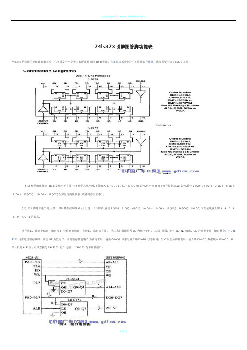
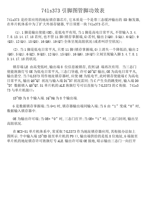
74ls373引脚图管脚功能表74ls373是常用的地址锁存器芯片,它实质是一个是带三态缓冲输出的8D触发器,在单片机系统中为了扩展外部存储器,通常需要一块74ls373芯片,(1).1脚是输出使能(OE),是低电平有效,当1脚是高电平时,不管输入3、4、7、8、13、14、17、18如何,也不管11脚(锁存控制端,G)如何,输出2(Q0)、5(Q1)、6(Q2)、9(Q3)、12(Q4)、15(Q5)、16(Q6)、19(Q7)全部呈现高阻状态(或者叫浮空状态);(2).当1脚是低电平时,只要11脚(锁存控制端,G)上出现一个下降沿,输出2(Q0)、5(Q1)、6(Q2)、9(Q3)、12(Q4)、15(Q5)、16(Q6)、19(Q7)立即呈现输入脚3、4、7、8、13、14、17、18的状态.锁存端LE 由高变低时,输出端8 位信息被锁存,直到LE 端再次有效。
当三态门使能信号OE为低电平时,三态门导通,允许Q0~Q7输出,OE为高电平时,输出悬空。
当74L S373用作地址锁存器时,应使OE为低电平,此时锁存使能端C为高电平时,输出Q0~Q7 状态与输入端D1~D7状态相同;当C发生负的跳变时,输入端D0~D7 数据锁入Q0~Q7。
51单片机的ALE信号可以直接与74LS373的C连接。
74ls373与单片机接口:1D~8D为8个输入端。
1Q~8Q为8个输出端。
G是数据锁存控制端;当G=1时,锁存器输出端同输入端;当G由“1”变为“0”时,数据输入锁存器中。
OE为输出允许端;当OE=“0”时,三态门打开;当OE=“1”时,三态门关闭,输出呈高阻状态。
在MCS-51单片机系统中,常采用74LS373作为地址锁存器使用,其连接方法如上图所示。
其中输入端1D~8D接至单片机的P0口,输出端提供的是低8位地址,G端接至单片机的地址锁存允许信号ALE。
输出允许端OE接地,表示输出三态门一直打开。
74ls373引脚图管脚功能表
74ls373引脚图管脚功效表74ls373是经常应用的地址锁存器芯片,它本质是一个是带三态缓冲输出的8D触发器,在单片机体系中为了扩大外部存储器,平日须要一块74ls373芯片,(1).1脚是输出使能(OE),是低电平有用,当1脚是高电日常平凡,不管输入3.4. 7.8.13.14.17.18若何,也不管11脚(锁存掌握端,G)若何,输出2(Q0).5(Q1).6(Q2).9 (Q3).12(Q4).15(Q5).16(Q6).19(Q7)全体呈现高阻状况(或者叫浮空状况);(2).当1脚是低电日常平凡,只要11脚(锁存掌握端,G)上消失一个降低沿,输出2 (Q0).5(Q1).6(Q2).9(Q3).12(Q4).15(Q5).16(Q6).19(Q7)立刻呈现输入脚3.4.7.8.1 3.14.17.18的状况.锁存端LE 由高变低时,输出端8 位信息被锁存,直到LE 端再次有用. 当三态门使能旌旗灯号OE为低电日常平凡,三态门导通,许可Q0~Q7输出,OE为高电日常平凡,输出悬空.当74LS373用作地址锁存器时,应使OE为低电平,此时锁存使能端C为高电日常平凡,输出Q0~Q7 状况与输入端D1~D7状况雷同;当C产生负的跳变时,输入端D0 ~D7 数据锁入Q0~Q7.51单片机的ALE旌旗灯号可以直接与74LS373的C衔接. 74ls3 73与单片机接口:1D~8D为8个输入端.1Q~8Q为8个输出端.G是数据锁存掌握端;当G=1时,锁存器输出端同输入端;当G由“1”变成“0”时,数据输入锁存器中.OE为输出许可端;当OE=“0”时,三态门打开;当OE=“1”时,三态门封闭,输出呈高阻状况.在MCS-51单片机体系中,常采取74LS373作为地址锁存器应用,其衔接办法如上图所示.个中输入端1D~8D接至单片机的P0口,输出端供给的是低8位地址,G端接至单片机的地址锁存许可旌旗灯号ALE.输出许可端OE接地,暗示输出三态门一向打开。
74LS373应用介绍
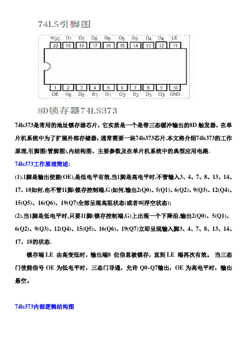
74ls373是常用的地址锁存器芯片,它实质是一个是带三态缓冲输出的8D触发器,在单片机系统中为了扩展外部存储器,通常需要一块74ls373芯片.本文将介绍74ls373的工作原理,引脚图(管脚图),内结构图、主要参数及在单片机系统中的典型应用电路.74ls373工作原理简述:(1).1脚是输出使能(OE),是低电平有效,当1脚是高电平时,不管输入3、4、7、8、13、14、17、18如何,也不管11脚(锁存控制端,G)如何,输出2(Q0)、5(Q1)、6(Q2)、9(Q3)、12(Q4)、15(Q5)、16(Q6)、19(Q7)全部呈现高阻状态(或者叫浮空状态);(2).当1脚是低电平时,只要11脚(锁存控制端,G)上出现一个下降沿,输出2(Q0)、5(Q1)、6(Q2)、9(Q3)、12(Q4)、15(Q5)、16(Q6)、19(Q7)立即呈现输入脚3、4、7、8、13、14、17、18的状态.锁存端LE 由高变低时,输出端8 位信息被锁存,直到LE 端再次有效。
当三态门使能信号OE为低电平时,三态门导通,允许Q0~Q7输出,OE为高电平时,输出悬空。
74ls373内部逻辑结构图74LS373的真值表(功能表),表中:L——低电平;H——高电平;X——不定态;Q0——建立稳态前Q的电平;G——输入端,与8031ALE连高电平:畅通无阻低电平:关门锁存。
图中OE——使能端,接地。
当G=“1”时,74LS373输出端1Q—8Q与输入端1D—8D相同;当G为下降沿时,将输入数据锁存。
74ls373引脚(管脚)排列图:74ls373电气特性74ls373推荐工作条件74ls373在单片机系统中的应用电路图:当74LS373用作地址锁存器时,应使OE为低电平,此时锁存使能端C为高电平时,输出Q0~Q7 状态与输入端D1~D7状态相同;当C发生负的跳变时,输入端D0~D7 数据锁入Q0~Q7。
51单片机的ALE信号可以直接与74LS373的C连接。
74hc373中文资料
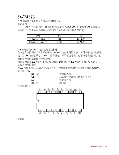
54/74373八D锁存器(3S,锁存允许输入有回环特性)简要说明:373为三态输出的八D透明锁存器,共有54/74S373和54/74LS373两种线路结构型式,其主要电器特性的典型值如下(不同厂家具体值有差别):型号t Pd P D54S373/74S373 7ns 525mW54LS373/74LS373 17ns 120mW373的输出端O0~O7可直接与总线相连。
当三态允许控制端OE为低电平时,O0~O7为正常逻辑状态,可用来驱动负载或总线。
当OE为高电平时,O0~O7呈高阻态,即不驱动总线,也不为总线的负载,但锁存器内部的逻辑操作不受影响。
当锁存允许端LE为高电平时,O随数据D而变。
当LE为低电平时,O被锁存在已建立的数据电平。
当LE端施密特触发器的输入滞后作用,使交流和直流噪声抗扰度被改善400mV。
引出端符号:D0~D7 数据输入端OE 三态允许控制端(低电平有效)LE 锁存允许端O0~O7 输出端外部管腿图:逻辑图:真值表:极限值:电源电压 (7V)输入电压54/74S373…………………………….………….5.5V54/74LS373…………………………………….7V输出高阻态时高电平电压 …………………………. 5.5V工作环境温度54XXX ………………………………….-55~125℃ 74XXX ………………………………….0~70℃存储温度 …………………………………………. -65~150℃推荐工作条件:54/74S373 54LS373/74LS373最小额定最大最小额定最大单位54 4.5 5 5.5 4.5 5 5.5电源电压Vcc74 4.75 5 5.25 4.75 5 5.25V 输入高电平电压V iH 2 2 V54 0.8 0.7输入低电平电压V iL74 0.8 0.8V54 -2 -1输出高电平电流I OH74 -6.5 -2.6mA54 20 12 输出低电平电流I OL74 20 24 mAwww.elecfans.comLE(H) 6 15脉冲宽度t w LE(L) 7.3 15 ns保持时间t H D 10↓ 10↓ ns 建立时间t set D 0↓0↓ns静态特性(TA 为工作环境温度范围) S373 LS373参 数测 试 条 件【1】最小 最大 最小 最大 单位V IK 输入嵌位电压 Vcc=最小,I ik =-18mA-1.5-1.5 VV OH 输出高电平电压Vcc =最小,V IL =最大,V IH =2V ,I OH =最大2.4 2.4 V54 0.5 0.4 V OL 输出低电平电压Vcc=最小,V IL =最大,V IH =2V,I OL =最大74 0.5 0.5 V V I =5.5V 1 I I 最大输入电压时输入电流Vcc =最大V I =7V 0.1 mA V IL =0.5V -0.25I IL 输入低电平电流 Vcc =最大,V IL =0.4V -0.4mA I IH 输入高电平电流 Vcc =最大,V IH =2.7V50 20 uA I OS 输出短路电流 Vcc =最大-40 -100 -30 -130 mA Icc 电源电流 Vcc =最大,OE 接4.5V160 40 mA V 0=2.4V 50 I OZH 输出高阻态时高电平电流 Vcc =最大,V IH =2VV 0=2.7V 20 mA V 0=0.5V-50 I OZL 输出高阻态时低电平电流Vcc =最大,V IH =2VV 0=0.4V-20 mA[1]: 测试条件中的“最小”和“最大”用推荐工作条件中的相应值。
74ls373中文资料

PD
m
54S373/74S373
7ns
54LS373/74LS373
17ns
525mW 120mW
r
a 373 的输出端 O0~O7 可直接与总线相连。
当三态允许控制端 OE 为低电平时,O0~O7 为正常逻辑状态,可用来驱动负载或总
- 线。当 OE 为高电平时,O0~O7 呈高阻态,即不驱动总线,也不为总线的负载,但
单位
VIK输入嵌位电压
VOH输出高电平电压
VOL输出低电平电压 II最大输入电压时输入
电流 IIL输入低电平电流 IIH输入高电平电流
Vcc=最小,Iik=-18mA
Vcc=最小,VIL=最大, VIH=2V,IOH=最大
Vcc=最小,VIL=最大, 54
VIH=2V,IOL=最大
74
Vcc=最大
VI=5.5V VI=7V
54LS373/74LS373 最小 额定 最大
单位
电源电压 Vcc
54 4.5
5
74 4.75
5
输入高电平电压ViH
2
输入低电平电压ViL
54 74
5.5
4.5
5
5.5
5.25 4.75
5
5.25
V
2
V
0.8 0.8
0.7 0.8
V
输出高电平电流IOH
54 74
-2
-1
mA
-6.5
-2.6
输出低电平电流IOL
. 输出高阻态时高电平电压 ………………………….
工作环境温度
w 54XXX
………………………………….
74XXX
………………………………….
HD74LS373PDIP中文资料

Hitachi Code JEDEC EIAJWeight (reference value)DP-20N —Conforms 1.26 gUnit: mm元器件交易网Cautions1.Hitachi neither warrants nor grants licenses of any rights of Hitachi’s or any third party’s patent,copyright, trademark, or other intellectual property rights for information contained in this document.Hitachi bears no responsibility for problems that may arise with third party’s rights, includingintellectual property rights, in connection with use of the information contained in this document.2.Products and product specifications may be subject to change without notice. Confirm that you have received the latest product standards or specifications before final design, purchase or use.3.Hitachi makes every attempt to ensure that its products are of high quality and reliability. However,contact Hitachi’s sales office before using the product in an application that demands especially high quality and reliability or where its failure or malfunction may directly threaten human life or cause risk of bodily injury, such as aerospace, aeronautics, nuclear power, combustion control, transportation,traffic, safety equipment or medical equipment for life support.4.Design your application so that the product is used within the ranges guaranteed by Hitachi particularly for maximum rating, operating supply voltage range, heat radiation characteristics, installationconditions and other characteristics. Hitachi bears no responsibility for failure or damage when used beyond the guaranteed ranges. Even within the guaranteed ranges, consider normally foreseeable failure rates or failure modes in semiconductor devices and employ systemic measures such as fail-safes, so that the equipment incorporating Hitachi product does not cause bodily injury, fire or other consequential damage due to operation of the Hitachi product.5.This product is not designed to be radiation resistant.6.No one is permitted to reproduce or duplicate, in any form, the whole or part of this document without written approval from Hitachi.7.Contact Hitachi’s sales office for any questions regarding this document or Hitachi semiconductor products.Hitachi, Ltd.Semiconductor & Integrated Circuits.Nippon Bldg., 2-6-2, Ohte-machi, Chiyoda-ku, Tokyo 100-0004, Japan Tel: Tokyo (03) 3270-2111 Fax: (03) 3270-5109Copyright ' Hitachi, Ltd., 1999. All rights reserved. Printed in Japan.Hitachi Asia Pte. Ltd.16 Collyer Quay #20-00Hitachi TowerSingapore 049318Tel: 535-2100Fax: 535-1533URLNorthAmerica : http:/Europe : /hel/ecg Asia (Singapore): .sg/grp3/sicd/index.htm Asia (Taiwan): /E/Product/SICD_Frame.htm Asia (HongKong): /eng/bo/grp3/index.htm Japan : http://www.hitachi.co.jp/Sicd/indx.htmHitachi Asia Ltd.Taipei Branch Office3F, Hung Kuo Building. No.167, Tun-Hwa North Road, Taipei (105)Tel: <886> (2) 2718-3666Fax: <886> (2) 2718-8180Hitachi Asia (Hong Kong) Ltd.Group III (Electronic Components)7/F., North Tower, World Finance Centre,Harbour City, Canton Road, Tsim Sha Tsui,Kowloon, Hong Kong Tel: <852> (2) 735 9218Fax: <852> (2) 730 0281 Telex: 40815 HITEC HXHitachi Europe Ltd.Electronic Components Group.Whitebrook ParkLower Cookham Road MaidenheadBerkshire SL6 8YA, United Kingdom Tel: <44> (1628) 585000Fax: <44> (1628) 778322Hitachi Europe GmbHElectronic components Group Dornacher Stra§e 3D-85622 Feldkirchen, Munich GermanyTel: <49> (89) 9 9180-0Fax: <49> (89) 9 29 30 00Hitachi Semiconductor (America) Inc.179 East Tasman Drive,San Jose,CA 95134 Tel: <1> (408) 433-1990Fax: <1>(408) 433-0223For further information write to:。
- 1、下载文档前请自行甄别文档内容的完整性,平台不提供额外的编辑、内容补充、找答案等附加服务。
- 2、"仅部分预览"的文档,不可在线预览部分如存在完整性等问题,可反馈申请退款(可完整预览的文档不适用该条件!)。
- 3、如文档侵犯您的权益,请联系客服反馈,我们会尽快为您处理(人工客服工作时间:9:00-18:30)。
4Q
GND
C†
† C for ’LS373 and ’S373; CLK for ’LS374 and ’S374.
5Q
5D
Schmitt-trigger buffered inputs at the enable/clock lines of the ’S373 and ’S374 devices simplify system design as ac and dc noise rejection is improved by typically 400 mV due to the input hysteresis. A buffered output-control (OC) input can be used to place the eight outputs in either a normal logic state (high or low logic levels) or the high-impedance state. In the high-impedance state, the outputs neither load nor drive the bus lines significantly.
SN54LS373, SN54LS374, SN54S373, SN54S374 . . . J OR W PACKAGE
SN74LS373, SN74S374 . . . DW, N, OR NS PACKAGE SN74LS374 . . . DB, DW, N, OR NS PACKAGE SN74S373 . . . DW OR N PACKAGE (TOP VIEW)
OC does not affect the internal operation of the latches or flip-flops. That is, the old data can be retained or new data can be entered, even while the outputs are off.
Please be aware that an important notice concerning availability, standard warranty, and use in critical applications of Texas Instruments semiconductor products and disclaimers thereto appears at the end of this data sheet.
SN74S374N
SN74S374N
Tube Tape and reel
SN74LS373DW SN74LS373DWR
LS373
0°C to 70°C
SOIC – DW
Tube Tape and reel Tube Tape and reel
SN74LS374DW SN74LS374DWR SN74S373DW SN74S373DWR
SN54LS373, SN54LS374, SN54S373, SN54S374,
SN74LS373, SN74LS374, SN74S373, SN74S374 OCTAL D-TYPE TRANSPARENT LATCHES AND EDGE-TRIGGERED FLIP-FLOPS
SDLS165B – OCTOBER 1975 – REVISED AUGUST 2002
SNJ54LS374W
Tube
SNJ54S374W
SNJ54S374W
Tube
SNJ54LS373FK SNJ54LS373FK
Tube LCCC – FK
Tube
SNJ54LS374FK SNJ54S373FK
SNJ54LS374FK SNJ54S373FK
Tube
SNJ54S374FK
SNJ54S374FK
ORDERING INFORMATION
TA
PACKAGE†
ORDERABLE PART NUMBER
TOP-SIDE MARKING
Tube
SN74LS373N
SN74LS373N
PDIP – N
Tube Tube
SN74LS374N SN74S373N
SN74LS374N SN74S373N
Tube
SNJ54LS374J SN54S373J
Tube
SNJ54S373J
SNJ54S373J
Tube
SN54S374J
SN54S374J
–55°C to 125°C
Tube
SNJ54S374J
SNJ54S374J
Tube
SNJ54LS373W
SNJ54LS373W
CFP – W
Tube
SNJ54LS374W
PRODUCTION DATA information is current as of publication date. Products conform to specifications per the terms of Texas Instruments standard warranty. Production processing does not necessarily include testing of all parameters.
Function Tables
’LS373, ’S373 (each latch)
INPUTS
OC
C
D
OUTPUT Q
L
H
H
H
L
H
L
L
L
L
X
Q0
H
X
X
Z
’LS374, ’S374 (each latch)
1
SN54LS373, SN54LS374, SN54S373, SN54S374,
SN74LS373, SN74LS374, SN74S373, SN74S374 OCTAL D-TYPE TRANSPARENT LATCHES AND EDGE-TRIGGERED FLIP-FLOPS
SDLS165B – OCTOBER 1975 – REVISED AUGUST 2002
74S374
SSOP – DB Tape and reel SN74LS374DBR LS374A
Tube
SN54LS373J
SN54LS373J
Tube
SNJ54LS373J
SNJ54LS373J
Tube
SN54LS374J
SN54LS374J
CDIP – J
Tube Tube
SNJ54LS374J SN54S373J
SN54LS373, SN54LS374, SN54S373, SN54S374 . . . FK PACKAGE (TOP VIEW)
8Q
VCC
OC
1Q
1D
2D
3 2 1 20 19
4
18
8D
2Q 5
17 7D
3Q 6
16 7Q
3D 7
15 6Q
4D 8
14 6D
9 10 11 12 13
The eight flip-flops of the ’LS374 and ’S374 are edge-triggered D-type flip-flops. On the positive transition of the clock, the Q outputs are set to the logic states that were set up at the D inputs.
† Package drawings, standard packing quantities, thermal data, symbolization, and PCB design guidelines are available at /sc/package.
2
• POST OFFICE BOX 655303 DALLAS, TEXAS 75265
OC 1 1Q 2 1D 3 2D 4 2Q 5 3Q 6 3D 7 4D 8 4Q 9 GND 10
20 VCC 19 8Q 18 8D 17 7D 16 7Q 15 6Q 14 6D 13 5D 12 5Q 11 C†
† C for ’LS373 and ’S373; CLK for ’LS374 and ’S374.
Improve Noise Rejection (’S373 and ’S374)
D P-N-P Inputs Reduce DC Loading on Data
Lines (’S373 and ’S374)
description
These 8-bit registers feature 3-state outputs designed specifically for driving highly capacitive or relatively low-impedance loads. The high-impedance 3-state and increased high-logic-level drive provide these registers with the capability of being connected directly to and driving the bus lines in a bus-organized system without need for interface or pullup components. These devices are particularly attractive for implementing buffer registers, I/O ports, bidirectional bus drivers, and working registers.