CC1瓷片电容规格书
低中高压瓷片陶瓷电容器资料规格书
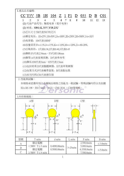
4.0
9.0
5.0 / 7.5
4.0
10.0
5.0 / 7.5
4.0
11.0
5.0 / 7.5
4.0
12.0
5.0 / 7.5
4.0
13.0
5.0 / 7.5
4.0
14.0
5.0 / 7.5
4.0
15.0
5.0 / 7.5
4.0
16.0
5.0 / 7.5
4.0
17.0
5.0 / 7.5
4.0
6.0
5.0 / 7.5
3. Stable capacitance change over the specified temperature.
Product Type
3. ( S - C ) 682PF ~ 224PF measured at 1KHz±10%, 0.1V rms, 25℃
Temp. Range
- 25 ℃ to + 85 ℃
Taping (Radial) -- Lead Spaciபைடு நூலகம்g F = 2.5 / 5.0 / 6.35 / 7.5 ± 0.8
D
s
s
D
H1 Ho
I
P P2
P1
Do Po
b
F
W2 d
W1 Wo w
t
P H1
P2 P1 Ho
Do
I
Po
W2 W1 Wo
s
s
F
d w
t
H1 Ho
I
Straoghe
≦7.0%
≦7.0%
+22% ~ -56% +22% ~ -82%
片式陶瓷电容规格书
Structure and Dimensions
L
T BW
W
Size Code 05 10
EIA Code 0402 0603
Dimension(mm) L 1.00 0.05 1.60 0.10 2.00 0.10 W 0.50 0.05 0.80 0.10 1.25 0.10 1.25 0.15 1.25 0.20 1.60 0.20 T 0.50 0.05 0.50+0.0/-0.1 0.80 0.10 0.85 0.10 1.25 0.10 1.25 0.15 1.25 0.20 0.60 0.10 0.85 0.15 0.85 0.10(*) 1.15 0.10 1.25 0.15 1.60 0.20 0.85 0.15 0.85 0.10(*) 0.90 0.10 1.60 0.20 1.80 0.20 2.00 0.20 2.50 0.20 2.50 0.30 2.00 0.20 3.20 0.30 3.20 0.30 Thickness Code 5 5 8 C F Q Y 6 C P F H C 9 H U I J v I L L 0.50 0.30 BW 0.2+0.15/-0.1 0.30 0.20
th
Spec(mm) 0.02 0.03 0.05 + 0.0/-0.1 0.10 0.10 0.10 0.15 0.10 0.15 0.2 0.15 * 0.10 0.15 0.10 0.10 0.15 0.20 0.15 * 0.10 0.10 0.10 0.20 0.15
Size
Code H U
0.40 0.40 0.40 0.40
2.50 2.00 3.20 5.00
0.30 0.20 0.30 0.40
多层片状陶瓷电容cm-cc

F
G
H
J
A
B
C
32 3225 1210 D
E
F
G
42 4520 1808
A B
A
B
43
4532 1812
C D
E
F
52 5720 2208 A
A
55 5750 2220 B
C
L 0.4±0.02 0.6±0.03 0.6±0.05 1.0±0.05
1.0±0.10 1.0±0.15 1.6±0.10 1.6±0.15 1.6±0.2
1.00 max.
1.40 max.
1.60 max.
1.6±0.15
0.30
2.20 max.
2.0±0.2
2.5±0.2
1.6 max. 2.2 max.
0.15
2.0 max.
2.0±0.2
2.5 max. 2.5±0.2
0.30
2.8 max.
2.8±0.2
2.2 max.
0.15
2.0 max.
※温度系数取决于20°C和85°C两点的测定值。
⑤静电电容值允差
温 度 补 偿 类
高 介 电 常 数 类
代号 A∗ B C D G∗ J K
允差 ±0.05pF ±0.1pF ±0.25pF ±0.5pF
±2% ±5% ±10%
静电容量的适用范围 C<0.5pF
代号 J∗
C≤5pF
K
C<10pF
M
Z
∗ :适用于CL系列
④公称静电电容值 代码 静电容量值 R50 0.5pF 1R0 1pF 101 100pF 103 10000pF 105 1μF 107 100μF
IBS综合电路板明细表

功率电阻 顶调 顶调 注意极性 注意极性
10
Q1,Q2,Q3,Q4,Q5,Q6,Q7,Q8,Q9,Q10,Q 11
11 三端稳压IC LM7805CT 12 双稳态振荡器 HEFCD4528BP 继电器 AJS1311F 13 14 15 16 17
直插端子 双排插针 单排插针 PCB
104 474 105
注意极性 注意极性 注意极性 注意极性 注意极性 注意极性
IBS综合电路板明 细表
标记 处数 更改文件号 签 名 标准化 日 期 图 样 标 记 数 量 比 例 设计
珠海普利德医疗设备 有限公司 PLD5000型X射线电视 系统
审 核 工 艺
批 日
准 期
V1.0
共 2 张
1:1
序 号
名称
规格型号
用
途
数 量 1 3 1 1 1 4 2 1 7 1 1 4 3 5 2 1 3 3 4 2 3 7 3 4 3 1 2 3 2 1 2 2 4 3 1 1 1 2
备
15 33 221 561 472 103 223 333
注
1
2 3
4
5
15P/50V CC1 33P/50V CC1 221/50V CC1 561/50V CC1 瓷片电容 472/50V CT1 103/50V CT1 223/50V CT1 333/50V CT1 104/50V CT1 独石电容 474/50V CT4 涤纶电容 105/63V CL21X 10UF/25V CD110 22UF/25V CD110 100UF/25V CD110 电解电容 220UF/25V CD110 470UF/25V CD110 1000UF/25V CD110 75Ω RJ14 100Ω RJ14 270Ω RJ14 820Ω RJ14 1K RJ14 1K2 RJ14 2K RJ14 2K2 RJ14 3K3 RJ14 4K7 RJ14 金属膜电阻 5K6 RJ14 6K2 RJ14 6K8 RJ14 10K RJ14 12K RJ14 15K RJ14 20K RJ14 27K RJ14 39K RJ14 68K RJ14 100K RJ14
台湾CCT承认书,CCT电容规格书

承認書APPROVAL SHEET零件名稱:積層陶瓷電容Description :Multi-Layer Chip CapacitorDATE :20020099/1201深圳市宸远科电子有限公司ChipCera Technology CO.,LTD 深圳市宝安区银田工业区A9栋厂房TEL :+86-7+86-7555555--29120592FAX :+86-7+86-7555555--29120593Reference No.:PD0PD091201912019120100000011Customer Customer::宸遠科技料號CCT Part Numbers客戶料號Customer Customer’’s Part Numbers 宸遠科技ChipCera Technology Co.,LTD 客戶承認Customer Customer’’s Approval 製表Prepared by 審查Checked by 核准Approved byEngineer QA Manager Vice G.M.Tolerance Capacitance for dielectricA=±0.05pF B=±0.10pF C=±0.25pF D=±0.50pF F=±1.0% G=±2.0% J=±5.0% K=±10% M=±20%NP0X7R X5R Y5V 10pF and below More than10pF100pF~1μF(101~105)1uf~100uf(105~107)10nF~10uF(103~106) B,C,D G,J J,K,M K,M M,ZProduct dimensions in mm.X7R SeriesX7R/X5R SeriesY5V Series7Resistance tosoldering heatPreheat the capacitor at120℃to150℃for1minute.Immerse the capacitor in an eutectic soldersolution at270270±±5℃for1010±±1seconds.After set it atroom temperature for2424±±2hours(temperaturecompensation type)or4848±±4hours(high dielectricconstant type),then measure.*High dielectric constant type:Initial measurement of X7RX7R/X5R/X5R and Y5V.Perform a heat treatment at150150±±5℃for one hourand then set it at room temperature for4848±±4hours.Perform the initial measurement.Dielectric NP0X7RX7R//X5RY5VAppearance No defectCapacitanceChange<±2.5%or<±0.25pF±7.5%±20%DF The same as No.2IRMore than500500ΩΩ-F(whichever is smaller)DielectricStrengthNo failure8Resistance toleachingThe capacitors are dipped into the solder at260260±±5℃for3030±±1seconds,and then check the solderingby measuring the areas covered with solder.95%of the terminations are to be soldered evenly andcontinuously.9Solder ability ofterminationZero hour test,and test after storage(20to24months)in original atmosphere in normalatmosphere;un-mounted chips completelyimmersed for2±0.5s in a solder bath of235±5℃.95%of the termination is to be soldered evenly andcontinuously.10Rapid change oftemperatureNPO/X7R:-55℃to+125℃,5cycleX5R:-55℃to+85℃,5cycleY5V:-25℃to+85℃,5cycleDuration:30mins.Recovery:24±2hrs.No visible damage after24h recoveryClass I NPO:∆C/C≤2.5%or±0.25pFClassⅡX7RX7R/X5R/X5R/X5R::∆C/C≤±15%Y5V:∆C/C≤±20%11Damp heat,steadystate500±12hours at40±2℃;90to95%RHNo visible damage after24±2(NPO)or48±4hoursrecoveryClassⅠ(NPO)1.∆C/C±5%or1pF,whichever is greater2.C<10pF;Q≥200+10C10≤C≤30pF;Q≥275+5/2CC>30pF;Q≥3503.IR≥4000MΩorRiCR≥4040ΩΩF,whichever is lessClassⅡ(X7R(X7R/X5R/X5R/X5R))1.∆C/C within±15%2.2.tantanδ≤7%3.3.R R≥2000MΩorRiCR≥5050ΩΩF,whichever is lessClassⅡ(Y5V)1.∆C/C within±30%2.50/25V:tanδ≤9%16V:tanδ≤12.5%10V:tanδ≤15%3.IR≥2000MΩorRiCR≥5050ΩΩF,whichever is less12Endurance 1000h at maximum temperatureVr(rated voltage)≤250VAt2×V rVr(rated voltage)=500VAt1.5VrVr(rated voltage)>500VAt1.2VrC>0..1UF,At1.5VrNo visible damage after24±2(NPO)or48±4hoursrecoveryClass1(NPO)1.∆C/C±2%or1pF,whichever is greater2.tanδ≤2x specified value3.IR≥4000MΩor RiCR≥4040ΩΩF,whichever is lessClass2(X7R(X7R/X5R/X5R/X5R))1.∆C/C within±15%2.tanδ≤7%3.IR≥2000MΩor RiCR≥5050ΩΩF,whichever is lessClass2(Y5V)1.∆C/C within±30%2.50/25V:tanδ≤9%16V:tanδ≤12.5%3.IR≥2000MΩor RiCR≥5050ΩΩF,whichever is lessAll dimensions in mmSize SymbolABPLT(Paper)T(Embossed)04020.62±0.05 1.12±0.05 2.00±0.058.00±0.200.60±0.05N/A 0603 1.10±0.10 1.90±0.10 4.00±0.108.00±0.20 1.00±0.05N/A 0805 1.65±0.05 2.40±0.05 4.00±0.108.00±0.20 1.00±0.05N/A 1206 2.00±0.10 3.50±0.10 4.00±0.108.00±0.20 1.00±0.05Max.2.01210 2.80±0.20 3.70±0.20 4.00±0.108.00±0.20N/A Max.2.01808 2.50±0.30 4.90±0.30 4.00±0.1012.0±0.20N/A Max.2.518123.60±0.304.90±0.308.00±0.1012.0±0.20N/AMax.2.5Paper Tape T ≦1.1mmEmbossed Tape T ≦2.60mm8.4+1.5/-0 All dimensions in mm6.1Capacitor ClassificationMulti-layer ceramic capacitors are available in wide range of characteristics.Electronic Industries Association (EIA)and the military have established categories to help divide the basic characteristics into more easily specified classes.The basic indu industrystry specification for ceramic capacitor is EIA specification RS-198and as noted in the general section,it specifies temperature-compensating capacitors as class I capacitors.These are specified by the military under specification MIL-C-20.General-pur General-purposepose capacitors with non-linear temperature coefficients are called Class II capacitors by EIA and specified by military under MIL-C-11015and MIL-C-39014.The new high reliability military specification,MIL-C-123covers both class Iand class II dielect dielectrics.rics.Class I —Class I capacitors or temperature-compensating capacitors are usually made from mixtures of titanates where barium titanate is normally not a major part of mix.They have predictable temperature coefficients and in general,do not have an aging characteristic.Thus they are the most stable capacitor available.Normally the T.C.s of Class I temperature-compensating capacitors are NP0(±30ppm/℃).Class II —General-purpose ceramic capacitors are called Class II capacitors and have become extremely popular because of the high capacitance values available in very small size.These capacitors are ferroelectrics and vary in capacitance value under the influence of the environmental and electrical operating conditions.Class II capacitors are affected by temperature 、voltage 、frequency and time.Temperature effects for Class II ceramic capacitors are exhibited as non-linear capacitancechanges with tem temperature.perature.Industry standards for Mid-K dielectrics,such as X7R X7R/X5R /X5R and High-K dielectrics,such as Z5U Z5U..6.2The Characterization of MaterialsThe T.C curve of each material (for reference)DesignationClass Temperature Range (℃)Temp.Characteristics NPO(COG)I -55~+125±30ppm/℃X7RII -55~+125±15%X5RII -55~+85±15%Y5V II -25~+85-82~+22%6.3Recommend IR reflow and wave solderng profile(Pb-Free)Typical profile band of IR reflow Typical profile band of wave soldering。
C系列TDK高压瓷片电容命名规格书

C Series Commercial Grade Mid Voltage (100 to 630V)
Type:
C1005 [EIA CC0402] C1608 [EIA CC0603] C2012 [EIA CC0805] C3216 [EIA CC1206] C3225 [EIA CC1210] C4532 [EIA CC1812] C5750 [EIA CC2220]
2. We may modify products or discontinue production of a product listed in this catalog without prior notification. 3. We provide “Delivery Specification” that explain precautions for the specifications and safety of each product
Notice: Effective January 2013, TDK will use a new catalog number which adds product thickness and packaging specification detail. This new catalog number should be referenced on all catalog orders going forward, and is not applicable for OEM part number orders. Please be aware the last five digits of the catalog number will differ from the item description (internal control number) on the product label. Contact your local TDK Sales representative for more information.
I类瓷片电容器规格
一、特性Ⅰ类瓷,也叫做温度补偿型(Temperature Compensating Type),是专门设计并用在低损耗、电容量稳定性高或要求温度系数有明确规定的谐振电路中的一种电容器例如,在电路中作温度补偿之用。
该类陶瓷介质是由标称温度系数(α)来确定。
其特性符合以下标准:用途:1). 谐振回路;2).对Q值要求高的电路;3).高稳定的容量特性。
二、温度系数、额定电压、静电容量关系表:温度特性NP0 SL N150 N220 N470 N750额定电压(VDC)50-200 50-200 500- 1000 2000 50-200 50-200 50-200 50-200标称容量范围(pF) 0.5 - 390 47 - 1000 22 - 680 18 - 470 12 - 220 15 - 220 20 - 270 15 - 470 测试条件 1MHz±20%, 1.0Vrms±0.2Vrms at 25± 2℃容量误差±0.25pF, ±0.5pF,±1%(C R:0.5pF ~10pF) ±5%, ±10%(C R>10pF)使用温度范围-25℃ ~+ 125℃Q值/DF值C R≥ 30pF: Q1000C R <30pF: Q400+20*C R;DF≤0.15%绝缘电阻Ri≥10000MΩU R (U R≥500VDC测试电压为500V DC ) 充电60S耐电压测试U R <1KV DC: 2.5U RU R≥1KV DC: 1.5U R +500V构造尺寸说明:(1).上图为标准引线长度、形式图形,但也可根据客户要求进行生产。
(2). C尺寸要求为:环氧树脂包封3.0mm 最大;酚醛树脂包封额定电压在250VDC以上者为2.0mm最大,否则为1.5mm 最大。
(3). D与T尺寸根据标称容量与额定电压大小决定,一般来说:同材质情况下,容量越大,D尺寸越大;额定电压越高,T尺寸越厚。
贴片电容型对照表三星国巨风华选型替代必备
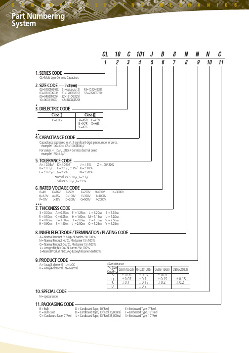
风华高科电容多层片式陶瓷电容0805 CG 104 J 500 N T1 2 3 4 5 6 71、尺寸2、介质种类3、标称电容量(PF)4、误差级别5、工作电压6、端头类别7、包装方式型号英寸毫米代码介质材料表示方法实际值代码误差表示方法实际电压标记端头材料标记包装0402 0.04*0.02 1.00*0.5 CG COG和NPO 100 10*100J ±5% 6R3 6.3V S 纯银T 编带0603 0.06*0.03 1.6*0.8 101 10*101G ±2% 100 10V C 纯铜 B 散装0805 0.08*0.05 2.00*1.25 102 10*102 C ±0.25PF 250 25V N 三层电镀1206 0.12*0.06 3.2*1.6 500 50V三星电容多层片式陶瓷电容CL 10 C 101 J B 8 N N N C1 2 3 4 5 6 7 8 9 10 11CL表示:多层陶瓷贴片电容2、尺寸3介质种类4、标称电容量(PF)5、误差级别6、工作电压7、厚度8端头类别型号英寸毫米代码介质材料表示方法实际值代码误差表示方法实际电压标记尺寸(mm)标记端头材料0402 0.04*0.02 1.00*0.5 CPRSTUL COGP2HR2HS2HT2HU2JS2L100 10*100 J ±5% R 4V 3 0.3 N 三层电镀0603 0.06*0.03 1.6*0.8 101 10*101 G ±2% Q 6.3V 4 0.50805 0.08*0.05 2.00*1.25 102 10*102 C ±0.25PF P 10V 89ACD0.8 0.9 0.650.851.001206 0.12*0.06 3.2*1.6 OALB 16V 25V 35V 50VAB Y F X X5RX7RX7SY5VX6SKMZ±10%±20%+80/-20%CDEFGHIJK100V200V250V350V500V630V1000V2000V3000V国巨(YAGEO)电容多层片式陶瓷电容CC ×××× × ×NPO ×BN ×××1 2 3 4 51、尺寸2、误差精度3、包装形式4、实际电压值5、标称电容量型号英制型号公制代码误差表示方法实际值代码电压代码实际值0201 0603 BCDFGJ±0.1PF±0.25PF±0.5PF±1%±2%±5%R 纸卷盘7inch 7 16V 100 10*1000402 1005 K 吸塑卷盘7inch 8 25V 101 10*101 0603 1608 P 纸卷盘13inch 9 50V 102 10*102 0805 2012 F 吸塑卷盘13inch1206 3216 C 散装1210 32251812 4532TDK贴片电容型号TDK贴片电容的参数识别C 2012 X7R 1H 104 K T系列名称体积材料电压容量误差包装0603=0201 CH 0J=6.3V C=0.25 T=卷带1005=0402 COG 1A=10V D=0.5 B=袋装1608=0603 JB 1C=16V J=5%2012=0805 JF 1E=25V K=10%3216=1206 X7R 1H=50V M=20%3225=1210 X5R 2A=100V Z=+80-20%4532=1812 Y5V 2E=250V5650=2220 2J=630V4520=1808 3A=1KV3D=2KV3F=3KV。
积层贴片陶瓷片式电容器商品说明书
此外,对使用本产品目录中所记载产品的设备进行设计时,请确保符合该设备的使用用途及状态的保护回路和装置,并设置备用回路等。 2. 本产品目录中记载的产品因改良及其他原因可能在不经预告的情况下进行变更或停止供应。 3. 关于本产品目录中记载的产品,本公司备有记载了各产品的规格及安全注意事项的 “ 交货规格书 ”。在选用产品时,建议签定交货规格
(例)
产品目录发行日期 2012 年12 月以前 2013 年1 月及以后
目录型号 C1608C0G1E103J(080AA) C1608C0G1E103J080AA
交货型号(交货标签上的标识) C1608C0G1E103JT000N C1608C0G1E103JT000N
20201025 / mlcc_commercial_general_zh.fm
长度 0.40 0.60 1.00 1.60 2.00 3.20 3.20 4.50 5.70
宽度 0.20 0.30 0.50 0.80 1.25 1.60 2.50 3.20 5.00
端子宽度 0.07 0.10 0.10 0.20 0.20 0.20 0.20 0.20 0.20
(3)温度特性
■系列概要
TDK积层陶瓷贴片电容器的C系列,是由诱电体材料以及内部电极、导电材料相互积层的表面贴装 (SMD)产品。单片式结构保证优异的机械强 度和高可靠性。 又因其简单的构造,跟其他种类电容相比具有更低的ESR、 ESL,频率特性良好。目前可以做到100uF的大容量,满足薄膜电容和电解电容的容 量领域。
C0G CH
JB
1C 1C 1C 1A 0J (16V) (16V) (16V) (10V) (6.3V)
0G (4V)
标准厚度 0.20 mm
CCT安规贴片电容规格书
Ex.: N: NPO X: X7R
110022
KK
550022
TT
SS
Capacitance Unit : pF Ex.: 100:10×100 471:47×101 182:18×102
Tolerance
Ex.: J :+/- 5% K :+/-10% M:+/-20%
Class
Ex.: 302: X2/Y3 502: X1/Y2 602: X1/Y2 for
CCT Series-Safety Capacitors
Multilayer Ceramic Chip Capacitors [ Safety Capacitor – X2Y3 & X1Y2 ]
CCT Series
The SCC series X2/Y3 & X1/Y2 safety capacitors are designed specifically for use in modem, facsimile, telephone and other electronic equipment.
NPO: 0 % ; X7R: 2.5 % per decade hr, Typical
Ú Electrical Strength : The Y2 class capacitor to meet the Australian safety requirement (passed 4200Vdc or 3000Vac Hi-Pot)
+A3: 1998 +A4: 2001
IEC 60950 : 2000
IEC 384-14: 1993 A1: 1995
UL 60950 : 2002 Third Edition
- 1、下载文档前请自行甄别文档内容的完整性,平台不提供额外的编辑、内容补充、找答案等附加服务。
- 2、"仅部分预览"的文档,不可在线预览部分如存在完整性等问题,可反馈申请退款(可完整预览的文档不适用该条件!)。
- 3、如文档侵犯您的权益,请联系客服反馈,我们会尽快为您处理(人工客服工作时间:9:00-18:30)。
d 10%
F 0.8 0.2
d 10%
F 0.8 0.2
d 10%
(b )
编带产品
2.5max 11max
2.5max 17min
2.5max
引脚距离和引线形式常规按EIA和JIS的标准执行。同时我们可以根据客户要求,做出符合客户使用习惯的引脚距离和引线形式。 NOTE: Lead style and distance are fit of JIS and EIA standard. Other we can produce with customers requirement.
1 15 1 30 22 50 47 68 70 82 86 100 100 120 120 150 ------
5 68 10 100 70 150 82 180 100 200 160 220 200 260 270 330 330 560
1 120 30 150 150 220 180 250 240 330 360 470 500 560 600 680 820 1000
8 容量允许偏差见EIA代码表: Capacitance tolerance, Please consider EIA code
代码
J
K
M
误差
S
Z
9 包装形式 Packing style 代码 symbol
T S
包装形式 盒带包装
散包装
Packing style Tape bulk
10 包封形式 Enclosure style 代码 code
E P
包封形式 环氧包封 酚醛包封
Enciosure style Epoxy resin Phenol resin
11.W- 表示无铅产品 Lead-Free 温度系数 TEMPERATURE CHARACTERISTICS
材料温度系数及允许偏差 :X10-6/ 0 60
750 120 140 1000
全符合要求,也不承诺一定按期交出。
跟进记录
□已联系客户
□ 已中止进行 □ 已建议生产
□ 中止原因描述: □ 已发送样品/日期
□ 客户已签收/日期
第1页共1页
【南京南山—领先的片式无源器件整合供应商】
订货方式 HOW TO ORDER
CC1 1
F
7
SL
1
B 331
J
S
P
294
4
直径 diameter(mm)
3.6-4.5
5 4.6-5.5
6 5.6-6.5
7 6.6-7.5
8 7.6-8.5
9 8.6-9.5
10
12
9.6-10.5 11.6-12.5
4 温度特性见温度系数及EIA代码表: Temperature coefficient:Please consider temperature characteristics and EIA code
工作电压 (UR)
operating voltage
50 500V
295
【南京南山—领先的片式无源器件整合供应商】
样品申请单
南山联系资料
总机:025-52188228 技术支持:025-84712971 客服:400-888-5058 传真:025-84710486 电邮:Tech@
5 瓷片电容引线形式 Lead style
代号 symbol
引线形式
1
直脚 (长20mm-28mm)b
2
直脚 (长16mm-19mm)b
3
切脚(短脚)
4
编带直脚型 (b )
5
编带小内弯型
6
编带大内弯型 (a )
7
特殊脚型 (b )
8
双外弯 (c )
9
外单弯(w )
0
前后弯 (b )
Style Straight lead (length 20mm) Straight lead (length 16mm)
试验电压 Test Voltage:2.5UR.
绝缘电阻 I.R:Insulation resistance Ri 10000M .
损耗角正切值 tangent of loss angel
5PF C 30PF, tg 1/(400 20C) C>30PF, tg 0.0015 C 5pF 时按照客户与生产商协商确定。 Please consult your requirements to factory
第二位数字
The Second Letter 5: 85 7: 125
第三位数字
The Third Letter
P: 10
R: 15
U: 22
56
V: 22
82
圆片瓷介电容外形尺寸 DIMENSIONS
散装产品 (a )
Dmax
Tmax
(b )
Dmax
Tmax
(C )
Dmax
Tmax
(b )
F 0.8 0.2
Cutting lead (short lead) Tape straight lead
Tape small inside kink Tape large inside kink
Special foot Double outside kinks
Outside kink Around the bend
于谐振回路及温度补偿效应的电路。 Low DF, stable capacitance, the linear capacitance change with
temperature. Designed from all series T.C suits for resonant circuit and temperature compensated circuit.
使用温度范围: 25
85
Operating Temperature Range:-250C +850C
电容量范围 Capacitance Range
DMax (mm) Dimension
NPO (CH)
容量范围 (Capacitance Range) PF
N750
SL
(UJ)
4.0 4.5 5.0 6.0 7.0 8.0 9.0 10.0 12.0
客户基本资料
公司名称 联系方式 收货地址 生产产品
联络人
电话:
姓名: 电话:
传真:
职务: 手机:
网址: □生产型企业
□贸易商
□技术 电邮:
□采购
□其他
样品明细资料元器件名称 来自号及封装单机用量 申请数量 备注
预计生产情况
预计小批量生产日期:
规模生产日期:
样品申请日期:
样品申请流程
1、请详细、全面、真实填写上列各项。表格不够填写,可自行复制。 2、请以附件的形式将该文档通过 E-mail 发送,并然请后将并此请单将打此印单盖打章印后盖,章传后真传至真:至02052-58-48741701408468。6。 3、公司将根据客户所填信息并综合相关情况,由样品小组负责确定该样品申请单是否执行及如何执行。 4、收到样品申请单并经审核通过后,南京库有现货2个工作日内发出;如需订货,交期3-4周,非常规品顺延1-2周。 5、样品免费,运费到付(一般选择顺丰快递);样品数量:单个型号5~20pcs, 或根据 BOM 表清单按2~5套提供。 6、说明:接单后,样品小组将努力跟进,但由于原厂生产等环节存有不确定因素,我们无法保证样品数量、型号完
292
【南京南山—领先的片式无源器件整合供应商】
CERAMIC DISC CAPACITOR
6 瓷片电容脚距 Lead Spacing
symbol A B D E
Lead spacing(mm) 2.5 0.5 5.0 0.5 7.5 0.5 10.0 0.5
7 瓷片电容标称容量 Standard capacitance
材料
NP0 N750 P140 N1000(SL)
EIA代码
C0H U2J S2L
JIS GB 代码
CH UJ or U2J SL or S2L
293
【南京南山—领先的片式无源器件整合供应商】
EIA代码 EIA CODE
第一位数字
The First Letter X:-55 Y:-30 Z: 10
W
2
3
4
5
6
7
8
9
10
11
1 产品类型 Capacitor Type Code
Type
低压温度补偿瓷介电容器
CC1
高压温度补偿瓷介电容器
CC81
低压高电介质常数瓷介电容器
CT1
高压高电介质常数瓷介电容器
CT81
半导体瓷介电容器
CS1
交流瓷介电容器
CT7
Low voltage temperature compensated disk ceramic capacitor High voltage temperature compensated disk ceramic capacitor Low voltage high dielectric constant disk ceramic capacitor High voltage high dielectric constant disk ceramic capacitor Semiconductor dielectric insulator disk ceramic capacitor Alternating current disk ceramic capacitor