Power MOSFET Basic and Application解析
MOSFET用作开关时的特性与计算方法

4.9功率型MOSFET用作开关(THE POWER MOSFET USED AS A SWITCH)4.9.1概论(Introduction)虽然场效应电晶体(field-effect transistor FET)应用于电路设计上己有许多年了,而近年来功率型金属氧化半导体场效应电晶体(metal-oxide-semiconductor field-effect transistor MOSFET),也己成功地制造出来,并在商业上大量的应用于功率电子的设计上。
而此MOSFET的功能需求,更超越了其它的功率组件,工作频率可达20kHz以上,一般都工作于100-200kHz,而不需像双极式功率电晶体有诸般经验上的限制。
当然,如果我们设计转换器工作于100 kHz频率下,比工作于20kHz的频率会有更多的优点,最重要的优点就是能减少体积大小与重量,功率型MOSFET提供设计者一种高速度,高功率,高电压,与高增益的组件,且几乎没有储存时间,没有热跑脱与被抑制的崩溃特性,由于不同的制造厂商会使用不同的技术来制造功率型的FET,因此就会有不同的名称,如HEXFET,VMOS,TMOS 等,此乃成为每一公司特有的注册商标。
虽然结构上会有所改变而增强了某些功能,但是所有的MOSFETs基本的工作原理都是相同的,事实上对某些应用上来说,使用特有型式的MOSFET有时亦会较使用其它型式来得适切引人些。
4.9.2基本MOSFET的定义(Basic MOSFET Definitions)MOSFET的电路符号示于图4-16中,此为N通道的MOSFET,在图4-16中另一个为NPN双极式电晶体,可互相参考比较其符号之不同,当然亦有P通道的MOSFET,其电路符号中的箭头方向刚好与N通道相反,在图4-16的这二个电路符号,双极式电晶体的集极,基极,与射极端,就相对于MOSFET的漏极,栅极与源极端。
虽然此二者组件都称为电晶体,可是我们必须明了,双极式组件与MOSFET,在结构上与操作原理上还是有明显的不同。
功率MOSFET的介绍
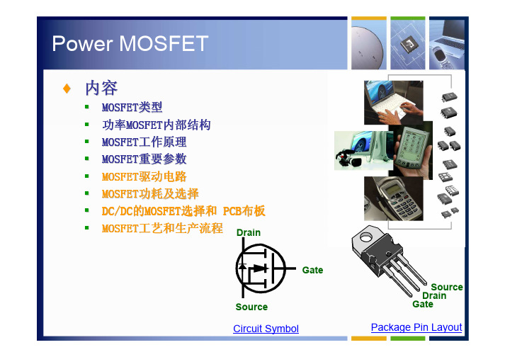
Power MOSFET♦ 内容MOSFET类型 功率MOSFET内部结构 MOSFET工作原理 MOSFET重要参数 MOSFET驱动电路 MOSFET功耗及选择 DC/DC的MOSFET选择和 PCB布板 MOSFET工艺和生产流程 DrainGate Source Drain GateSourceCircuit SymbolPackage Pin LayoutPower MOSFET♦ 什么是MOSFET,定义MOSFET ♦ Metal - Oxide – Semiconductor Field Effect Transistor ♦ MOSFET is a three-terminal devices which in basic term behaves as a voltage controlled switchDrainGate Source Drain GateSourceCircuit SymbolPackage Pin LayoutPower MOSFET♦ 氧化层:形成门极,由多晶硅代替 氧化层:形成门极, ♦ 氧化隔离层:防止电流在门极和其它两个电极间D、S极流动,但并不阻 氧化隔离层: 极流动, 断电场 ♦ 半导体层:依赖于门极电压,阻断或允许电流在漏极D和源极S间流动 半导体层:依赖于门极电压,Power MOSFET♦ MOSFET类型 Metal Oxide Semiconductor Field Effect Transistor按导电沟道可分为: 按导电沟道可分为:P沟道和N沟道 按栅极电压幅值可分为: 按栅极电压幅值可分为: 栅极电压为零时, 耗尽型--栅极电压为零时,漏源极之间就存在导电沟道 沟道器件,栅极电压大于(小于) 增强型--对于N(P)沟道器件,栅极电压大于(小于)零时才存在导电沟道 功率MOSFET主要是N沟道增强型1Power MOSFET♦ MOSFET内部结构横向导电(信号MOSFET)/垂直导电(功率MOSFET) 垂直导电:平面型和沟槽型Trench(U型沟槽和V型沟槽) 不同厂商制造的功率MOSFET有不同的命名:HEXFET (IR)、VMOS (Phillips)、 SIPMOS (Siemens),但都是通过将大量物理单元扩散到外延硅基板形成并联结 构的方法制成 功 率 MOSFET 为 多 单 元 集 成 结 构 , 如 IR 的 HEXFET 采 用 六 边 形 单 元 ; 西 门 子 Siemens的SIPMOSFET采用正方形单元;摩托罗拉公司Motorola的TMOS采用矩形 单元按品字形排列 横向导电:平面型 垂直导电:V型沟槽 垂直导电:平面型 垂直导电:U型沟槽Power MOSFET♦ 平面型MOSFET 没有充分应用芯片的尺寸, 没有充分应用芯片的尺寸,电流和电压额定值有限 适合低压应用,如微处理器,运放,数字电路 适合低压应用,如微处理器,运放, 低的电容, 低的电容,快的开关速度增加或减少门极电压会增大或减少N沟道的大小,以此来控制器件导通 沟道的大小, VddLoadDDriverG S沟道Power MOSFET♦ 垂直导电型MOSFET平面型:具有垂直导电双扩散 MOS 结构的 VDMOSFET Vertical Double-diffused MOSFET ,多个单元结构。
Infineon pspice MOSFET模型使用

Introduction to Infineon’s Simulation Models Power MOSFETs
IFAT PMM F. Stueckler G. Noebauer K. Bueyuektas
Simulation models for Infineon Power MOSFET
Simulation models for Infineon Power MOSFET
Application Note AN 2014-02 V2.0 Feb. 2014
1 Introduction
Models provided by Infineon are not warranted by Infineon as fully representing all the specifications and operating characteristics of the semiconductor product to which the model relates. The models describe the characteristics of typical devices. In allห้องสมุดไป่ตู้cases, the current data sheet information for a given device is the final design guideline and the only actual performance specification. Although models can be a useful tool in evaluating device performance, they cannot model exact device performance under all conditions, nor are they intended to replace breadboarding for final verification. Infineon therefore does not assume any liability arising from their use. Infineon reserves the right to change models without prior notice.
the power mosfet 应用手册

the power mosfet 应用手册The Power MOSFET Application ManualIntroductionThe Power MOSFET Application Manual is a comprehensive guide that delves into the various applications and uses of Power MOSFETs. This manual aims to provide engineers, designers, and enthusiasts with an in-depth understanding of Power MOSFETs, their characteristics, and how they can be effectively implemented in different electronic systems.Section 1: Understanding Power MOSFETs1.1 What is a Power MOSFET?Power MOSFETs, or Metal-Oxide-Semiconductor Field-Effect Transistors, are electronic devices that offer high efficiency, fast switching speeds, and excellent power handling capabilities. This section delves into the structure and functioning of Power MOSFETs, explaining how they differ from their bipolar transistor counterparts.1.2 MOSFET Characteristics and SpecificationsThis subsection explores the various specifications and characteristics of Power MOSFETs, including voltage ratings, current ratings, on-resistance, gate charge, and thermal considerations. It provides engineers with the necessary knowledge to select the appropriate MOSFETs for different applications.Section 2: Power MOSFET Applications2.1 Switching ApplicationsPower MOSFETs have found extensive use in switching applications, such as motor drives, power supplies, and inverters. This section highlights the advantages of using Power MOSFETs in these applications and provides guidelines for circuit design, gate drive requirements, and considerations for minimizing power losses.2.2 Audio AmplificationPower MOSFETs are also commonly used in audio amplifiers due to their low distortion and high power capabilities. This subsection discusses the design considerations for audio amplifiers, including load matching, biasing, and output protection. It provides engineers with the necessary information to design efficient and high-quality audio amplifiers.2.3 Lighting ApplicationsPower MOSFETs are vital components in various lighting applications, including LED drivers, automotive lighting, and streetlights. This section explores the key considerations for designing lighting circuits using Power MOSFETs, including thermal management, dimming techniques, and EMI suppression.2.4 Power SuppliesPower MOSFETs play a crucial role in power supply designs, offering high efficiency and compact size. This subsection discusses the use of Power MOSFETs in different power supply topologies, such as buck converters, boost converters, and flyback converters. It also addresses the challenges ofdesigning power supplies with Power MOSFETs and provides guidelines for achieving optimal performance.Section 3: Protection and Reliability3.1 Overcurrent and Overvoltage ProtectionTo ensure the reliable operation of circuits using Power MOSFETs, adequate protection mechanisms must be implemented. This section covers the different protection techniques, such as overcurrent and overvoltage protection circuits, along with their advantages and limitations.3.2 Thermal ManagementProper thermal management is essential for preventing Power MOSFETs from overheating and ensuring their longevity. This subsection discusses the thermal behavior of Power MOSFETs and presents various cooling techniques, such as heatsinks, thermal vias, and thermal pads, to efficiently dissipate heat.3.3 ESD ProtectionElectrostatic Discharge (ESD) can pose a significant threat to Power MOSFETs and other sensitive electronic components. This section provides an overview of ESD protection methods and highlights the importance of implementing proper ESD protection measures in Power MOSFET applications.ConclusionThe Power MOSFET Application Manual aims to equip engineers, designers, and enthusiasts with the knowledge and skills necessary toeffectively utilize Power MOSFETs in their electronic designs. By providing insights into the characteristics, applications, and protection considerations, this manual serves as a valuable resource for those looking to optimize the performance and reliability of their circuits.。
NCE40H21 Pb Freepower MOSFET产品说明书
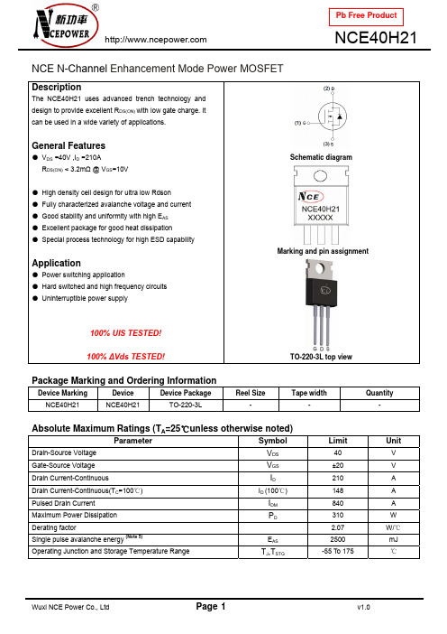
NCE N-Channel Enhancement Mode Power MOSFETDescriptionThe NCE40H21 uses advanced trench technology and design to provide excellent R DS(ON) with low gate charge. It can be used in a wide variety of applications.General Features● V DS =40V ,I D =210AR DS(ON) < 3.2m Ω @ V GS =10V● High density cell design for ultra low Rdson ● Fully characterized avalanche voltage and current ● Good stability and uniformity with high E AS ● Excellent package for good heat dissipation ● Special process technology for high ESD capabilityApplication● Power switching application● Hard switched and high frequency circuits ● Uninterruptible power supply100% UIS TESTED!100% ∆Vds TESTED!Schematic diagramMarking and pin assignmentTO-220-3L top viewPackage Marking and Ordering InformationDevice MarkingDeviceDevice PackageReel SizeTape widthQuantityNCE40H21 NCE40H21 TO-220-3L-- -Absolute Maximum Ratings (T A =25℃unless otherwise noted)Parameter Symbol Limit UnitDrain-Source Voltage V DS 40 V Gate-Source Voltage V GS ±20 V Drain Current-ContinuousI D 210 ADrain Current-Continuous(T C =100℃) I D (100℃) 148 A Pulsed Drain Current I DM 840 A Maximum Power Dissipation P D 310 W Derating factor2.07 W/℃Single pulse avalanche energy (Note 5)E AS 2500mJ Operating Junction and Storage Temperature RangeT J ,T STG-55 To 175℃Thermal CharacteristicThermal Resistance,Junction-to-Case (Note 2)R θJC0.48/W ℃Electrical Characteristics (T A =25℃unless otherwise noted)ParameterSymbolCondition Min Typ Max UnitOff CharacteristicsDrain-Source Breakdown Voltage BV DSS V GS =0V I D =250μA 40 - V Zero Gate Voltage Drain Current I DSS V DS =40V,V GS =0V -- 1 μA Gate-Body Leakage Current I GSS V GS =±20V,V DS =0V - - ±100 nA On Characteristics (Note 3) Gate Threshold VoltageV GS(th) V DS =V GS ,I D =250μA 1.3 1.8 2.5 V Drain-Source On-State Resistance R DS(ON) V GS =10V, I D =20A - 2.3 3.2 m ΩForward Transconductance g FSV DS =5V,I D =20A -100 - S Dynamic Characteristics (Note4) Input Capacitance C lss - 10331 - PFOutput CapacitanceC oss - 1160 - PFReverse Transfer Capacitance C rssV DS =25V,V GS =0V,F=1.0MHz- 1045 - PF Switching Characteristics (Note 4) Turn-on Delay Time t d(on) - 41 - nSTurn-on Rise Time t r - 40 - nS Turn-Off Delay Time t d(off) - 145 - nSTurn-Off Fall Time t fV DD =30V,R L =15Ω, R G =2.5Ω,V GS =10V - 65 - nSTotal Gate Charge Q g - 239 - nC Gate-Source Charge Q gs - 23.5 - nCGate-Drain ChargeQ gd I D =20A,V DD =20V,V GS =10V - 49.6 -nCDrain-Source Diode Characteristics Diode Forward Voltage (Note 3) V SDV GS =0V,I S =20A -0.85 1.2 V Diode Forward Current (Note 2)I S - - 210 A Reverse Recovery Time t rr - 55 nS Reverse Recovery Charge Qrr T J = 25°C, I F = 20Adi/dt = 100A/μs(Note3)- 90nCForward Turn-On Timet onIntrinsic turn-on time is negligible (turn-on is dominated by LS+LD)Notes:1. Repetitive Rating: Pulse width limited by maximum junction temperature.2. Surface Mounted on FR4 Board, t ≤ 10 sec.3. Pulse Test: Pulse Width ≤ 300μs, Duty Cycle ≤ 2%.4. Guaranteed by design, not subject to production5. EAS condition :Tj=25℃,V DD =20V,V G =10V,L=0.5mH,Rg=25ΩNCE40H21 Test circuit1)E AS test Circuits2)Gate charge test Circuit:3)Switch Time Test Circuit:Typical Electrical and Thermal Characteristics (Curves)Vds Drain-Source Voltage (V)Figure 1 Output CharacteristicsVgs Gate-Source Voltage (V)Figure 2 Transfer CharacteristicsI D- Drain Current (A)Figure 3 Rdson- Drain CurrentT J-Junction Temperature(℃)Figure 4 Rdson-JunctionTemperatureQg Gate Charge (nC)Figure 5 Gate ChargeVsd Source-Drain Voltage (V)Figure 6 Source- Drain Diode Forward RdsonOn-Resistance(mΩ)ID-DrainCurrent(A)ID-DrainCurrent(A)NormalizedOn-ResistanceVgsGate-SourceVoltage(V)Is-ReverseDrainCurrent(A)Vds Drain-Source Voltage (V)Figure 7 Capacitance vs VdsVds Drain-Source Voltage (V)Figure 8 Safe Operation AreaT J -Junction Temperature(℃)Figure 9 Power De-ratingT J -Junction Temperature(℃)Figure 10 Current De-ratingI D - D r a i n C u r r e n t (A )C C a p a c i t a n c e (p F )Square Wave Pluse Duration (sec)Figure 11 Normalized Maximum Transient Thermal Impedancer (t ),N o r m a l i z e d E f f e c t i v e T r a n s i e n t T h e r m a l I m p e d a n c eP o w e r D i s s i p a t i o n (W )I D - D r a i n C u r r e n t (A )TO-220-3L Package InformationDimensions In Millimeters Dimensions In Inches SymbolMin.Max.Min.Max.A 4.400 4.600 0.173 0.181A1 2.250 2.550 0.089 0.100b 0.710 0.910 0.028 0.036b1 1.170 1.370 0.046 0.054c 0.330 0.650 0.013 0.026c1 1.200 1.400 0.047 0.055D 9.910 10.250 0.390 0.404E 8.9500 9.750 0.352 0.384E1 12.650 12.950 0.498 0.510e 2.540 TYP. 0.100 TYP.e1 4.980 5.180 0.196 0.204F 2.650 2.950 0.104 0.116H 7.900 8.100 0.311 0.319h 0.000 0.300 0.000 0.01213.400 0.508 0.528L 12.900L1 2.850 3.250 0.112 0.128 V 7.500 REF. 0.295 REF.Φ 3.400 3.800 0.134 0.150Attention:■Any and all NCE power products described or contained herein do not have specifications that can handle applications that require extremely high levels of reliability, such as life-support systems, aircraft's control systems, or other applications whose failure can be reasonably expected to result in serious physical and/or material damage. Consult with your NCE power representative nearest you before using any NCE power products described or contained herein in such applications.■ NCE power assumes no responsibility for equipment failures that result from using products at values that exceed, even momentarily, rated values (such as maximum ratings, operating condition ranges, or other parameters) listed in products specifications of any and all NCE power products described or contained herein.■Specifications of any and all NCE power products described or contained herein stipulate the performance, characteristics, and functions of the described products in the independent state, and are not guarantees of the performance, characteristics, and functions of the described products as mounted in the customer’s products or equipment. To verify symptoms and states that cannot be evaluated in an independent device, the customer should always evaluate and test devices mounted in the customer’s products or equipment.■ NCE power Semiconductor CO.,LTD. strives to supply high-quality high-reliability products. However, any and all semiconductor products fail with some probability. It is possible that these probabilistic failures could give rise to accidents or events that could endanger human lives, that could give rise to smoke or fire, or that could cause damage to other property. When designing equipment, adopt safety measures so that these kinds of accidents or events cannot occur. Such measures include but are not limited to protective circuits and error prevention circuits for safe design, redundant design, and structural design.■ In the event that any or all NCE power products(including technical data, services) described or contained herein are controlled under any of applicable local export control laws and regulations, such products must not be exported without obtaining the export license from the authorities concerned in accordance with the above law.■No part of this publication may be reproduced or transmitted in any form or by any means, electronic or mechanical, including photocopying and recording, or any information storage or retrieval system, or otherwise, without the prior written permission of NCE power Semiconductor CO.,LTD.■Information (including circuit diagrams and circuit parameters) herein is for example only ; it is not guaranteed for volume production. NCE power believes information herein is accurate and reliable, but no guarantees are made or implied regarding its use or any infringements of intellectual property rights or other rights of third parties.■ Any and all information described or contained herein are subject to change without notice due to product/technology improvement, etc. When designing equipment, refer to the "Delivery Specification" for the NCE power product that you intend to use.■This catalog provides information as of Sep.2010. Specifications and information herein are subject to change without notice.。
mos场效应管简介及原理(英文)
MOS场效应管简介及原理(英文)【简介】MOS场效应晶体管(Metal-Oxide-Semiconductor Field-Effect Transistor)是一种常用于电子电路的晶体管。
它是一种小型、高度集成的设备,能够控制通过它的电流流动。
MOSFET被广泛应用于数字和模拟电子学、通信系统和电力电子等领域。
【原理】MOSFET的基本工作原理是通过在栅极电极施加电压来控制通过源极和漏极的电导。
通过栅极施加的电压决定了通过MOSFET的电流量。
MOSFET有两种类型:N型(负型)和P型(正型)。
N 型MOSFET的基板材料为n型半导体材料(含电子),而P 型MOSFET的基板材料为p型半导体材料(含空穴)。
这些材料的选择取决于应用,因为它们具有不同的电气特性。
MOSFET在电子电路中广泛应用,因为它们具有小型化、高速度和低功耗等优点。
它们还可以使用现代半导体制造技术轻松制造,使其成本效益高,并且广泛可用。
【英文】MOSFET (Metal-Oxide-Semiconductor Field-Effect Transistor) is a type of transistor commonly used in electronic circuits. It is a small, highly integrated device that can control the flow of electrical current through it. MOSFETs are used in awide range of applications, including digital and analog electronics, communication systems, and power electronics.The basic principle of operation of a MOSFET is that it controls the flow of electrical current through the gate electrode, which is insulated from the source and drain by a thin oxide layer. When a voltage is applied to the gate electrode, a current flows through the channel between the source and drain, causing the MOSFET to conduct electricity. The voltage applied to the gate electrode determines the amount of current that flows through the MOSFET.There are two main types of MOSFETs: N-type (for negative) and P-type (for positive). N-type MOSFETs have an n-type semiconductor material (containing electrons) as the substrate, while P-type MOSFETs have a p-type semiconductor material (containing holes) as the substrate. These types of materials are chosen based on the application, as they have different electrical properties.MOSFETs are widely used in electronic circuits because of their small size, high speed, and low power consumption. They are also easy to fabricate using modern semiconductor manufacturing techniques, making them cost-effective and widely available.。
power mosfet概述

Power MOSFET中文是电力场效应晶体管的意思。
电力场效应晶体管分为两种类型,结型和绝缘栅型,但通常所说的是绝缘栅型中的MOS型(Metal Oxide Semiconductor FET),简称电力MOSFET(Power MOSFET)。
P-MOSFET是用栅极电压来控制漏极电流,它的显著特点是驱动电路简单,驱动功率小,开关速度快,工作频率高;但是其电流容量小,耐压低,只用于小功率的电力电子装置,其工作原理与普通MOSFET一样。
特性Power MOSFET的主要特性如下:Power MOSFET静态特性主要指输出特性和转移特性, 与静态特性对应的主要参数有:漏极击穿电压;漏极额定电压;漏极额定电流和栅极开启电压等。
1、静态特性(1) 输出特性即是漏极的伏安特性曲线,如图2(b)所示.由图所见,输出特性分为截止,饱和与非饱和3个区域,这里饱和、非饱和的概念与GTR 不同。
饱和是指漏极电流ID 不随漏源电压UDS的增加而增加,也就是基本保持不变;非饱和是指地UCS一定时,ID 随UDS 增加呈线性关系变化.(2) 转移特性表示漏极电流ID与栅源之间电压UGS的转移特性关系曲线, 如图2(a) 所示. 转移特性可表示出器件的放大能力, 并且是与GTR 中的电流增益β相似。
由于Power MOSFET是压控器件,因此用跨导这一参数来表示,跨导定义为(1) 图中UT 为开启电压,只有当UGS=UT时才会出现导电沟道,产生漏极电流ID。
2、动态特性动态特性主要描述输入量与输出量之间的时间关系,它影响器件的开关过程。
由于该器件为单极型,靠多数载流子导电,因此开关速度快,时间短,一般在纳秒数量级。
Power MOSFET的动态特性.如图所示。
Power MOSFET栅极电阻;RL为漏极负载电阻;RF用以检测漏极电流。
Power MOSFET的开关过程波形,如图3(b)所示。
Power MOSFET的开通过程;由于Power MOSFET有输入电容,因此当脉冲电压up的上升沿到来时,输入电容有一个充电过程,栅极电压uGS 按指数曲线上升.当uGS 上升到开启电压UT 时,开始形成导电沟道并出现漏极电流iD.从up 前沿时刻到uGS=UT,且开始出现iD 的时刻,这段时间称为开通延时时间td(on).此后,iD 随uGS 的上升而上升,uGS 从开启电压UT 上升到Power MOSFET临近饱和区的栅极电压uGSP 这段时间,称为上升时间tr.这样Power MOSFET的开通时间ton=td(on)+tr(2)Power MOSFET 的关断过程:当up 信号电压下降到0 时,栅极输入电容上储存的电荷通过电阻RS 和RG 放电,使栅极电压按指数曲线下降,当下降到uGSP 继续下降,iD 才开始减小,这段时间称为关断延时时间td(off).此后,输入电容继续放电,uGS 继续下降,iD 也继续下降,到uGS<u< span="" style="margin: 0px; padding: 0px; list-style-type: none;">T 时导电沟道消失,iD=0, 这段时间称为下降时间tf.这样Power MOSFET 的关断时间toff=td(off)+tf (3)从上述分析可知,要提高器件的开关速度,则必须减小开关时间.在输入电容一定的情况下,可以通过降低驱动电路的内阻RS 来加快开关速度. 电力场效应管晶体管是压控器件,在静态时几乎不输入电流.但在开关过程中,需要对输入电容进行充放电,故仍需要一定的驱动功率.工作速度越快,需要的驱动功率越大。
PowerMos Process Flow Presentation

30VP
60VP 20VP 40VP
nutch
lasermark nutch
PAD氧化300-B
步骤 PAD氧化300-B PAD进后PARTICLE测量 厚度測量-PADOX
PU Type GATEOX SURFSCAN ELLISO
Major parameter 2.RDS(on)=Rsource + Rch + RA+ RD + Rsub + Rwcml
Rsource=Source diffusion resistance Rch=Channel resistance RA=Accumulation resistance
RD=Drift region resistance
PU Type
WS ADE LASERMARK RCAA
程序1
程序2
. . PRO RCAA20F2FM
Wafer specification N-EPI: 0.14R5.0T-Wacker N-EPI: 0.14R5T-Wacker N-EPI: 0.2R5.5T-Wacker N-EPI: 0.32R7.0T-Wacker N-EPI: 0.68R8.8T-Wacker P-EPI: 0.65R6.7T-Wacker P-EPI: 0.65R6.7T-Wacker P-EPI: 0.5R6.5T-Wacker P-EPI: 1.8R9.0T-Wacker P-EPI: 0.35R6.0T-Wacker P-EPI: 0.68R7.3T-Wacker
程序1
*RETICLE *RLAYERD . . DESCUM30 BOE-360S .
- 1、下载文档前请自行甄别文档内容的完整性,平台不提供额外的编辑、内容补充、找答案等附加服务。
- 2、"仅部分预览"的文档,不可在线预览部分如存在完整性等问题,可反馈申请退款(可完整预览的文档不适用该条件!)。
- 3、如文档侵犯您的权益,请联系客服反馈,我们会尽快为您处理(人工客服工作时间:9:00-18:30)。
1 2
4
Power MOSFET
Qrr~0.5 trr*Irrm
ISD
并联二极管/寄生晶体管
Irrm MOSFET结构所附带的本征二极管具有一定的雪崩能力。通常用单次雪崩能力和重复雪崩能力来表达。当反向di/dt很大时,二极 管会承受一个速度非常快的脉冲尖刺,它有可能进入雪崩区,一旦超越其雪崩能力就有可能将器件损坏。当电流迅速下降时,二 极管有一阶段失去反向阻断能力,即所谓反向恢复时间。PN结要求迅速导通时,也会有一段时间并不显示很低的电阻。
Ciss = CGD + CGS Coss = CDS + CGD Crss = CGD
总栅极电荷 :Qg 栅-源电荷:Qgs 栅-漏电荷:Qgd
Power MOSFET
♦ 阻性负载开关
Power MOSFET
IDS [A]
6
5
VT
4
VG=0
3
2
VD
1
ID=0
0 0 1 2 3 4 500
VDS [V]
电流流动垂直
Power MOSFET
♦ 垂直导电型MOSFET
平面型:电流电压与通道长,宽的大小相关. 平面型MOS饱和区特性比沟 槽型好. 沟槽型:元件面积与电流成正比,Epitaxial Layer厚度与电压成正比. 反转层:Inversion Layer DMOS:双重扩散MOS, Double Diffused MOS 是 多 子 单 极 型 器 件 ( 无 少 子 ), 因 此 受 温 度 影 响 小 ,PMOS 多 子 是 空 穴,NMOS多子是电子, Majority Carrier 氧化层相当于介电质 Dielectric Material (Dielectric constant), 掺杂 Doged, 高掺杂浓度区域 Heavily doped region.
寄生三极管导通,栅极失控,器件的击穿电 压从BVCBO减小到BVCEO ,约为50~60%的 BVCBO.如果加在漏极电压高于BVCEO,器件将 进入雪崩击穿.如果漏极电流不被外部限制, 器件将会被寄生三极管的二次击穿损坏。
Power MOSFET
♦ 寄生三极管
n+/p-体内的结正偏,寄生三极管导通,栅极失控 能力由单元尺寸,收缩处电阻 Rp和结合处电阻Rc及NPN增益决定 高温导致低的Vbe和高的电阻M MOSFET设计过程中采取措施使寄生晶体管尽量不起作用。不同功率 MOSFET措施各有不同,总的原则:使漏极的横向电阻RB尽量小。 因为只有在漏极N区的横向电阻流过足够电流为这个N区建立正偏的 条件时,寄生的双极晶体管才开始起作用。然而在严峻的动态条件下, 因dv/dt通过相应电容引起的横向电流有可能足够大,此时寄生双极晶 体管就会起动,有可能损坏MOSFET。所以考虑瞬态性能时对功率 MOSFET器件内部的各个电容(它是dv/dt的通道)都必须予以注意 这种现象可以由UIS,二极管的反向恢复,大的dV/dt和接触效应所触 发。
Power MOSFET
MOSFET的静态参数
♦ 热阻
此参数表明热量从A点到B点流动的难易程度。 小RTH表明热量从A点流 动到B点时,产生很小的温度差异。大的RTH表明当同样的热量从A点流 动到B点时,产生很大的温度差异。热阻定义为:
Rth( B A)
TB TA Pdiss
功率MOSFET基础
AOS上海应用中心 刘松
Power MOSFET
♦ 内容
功率MOSFET内部结构 MOSFET工作原理 MOSFET重要参数
Drain
Gate Source Drain Gate
Source
Circuit Symbol
Package Pin Layout
Power MOSFET
转移特性
输出特性
Power MOSFET
D
G
MOSFET的avalanche击穿电压总是大于标注的额定电压由于正 常生产中的余量控制
为了保证可靠性,在最坏的工作条件下,工作电压不要大于额定值。最大的 电压不要超过额定值的70~90%,降额使用。
S
Tracer waveform
结温升高,BV 线性增加
Power MOSFET
D
G
S
阈值电压VGS(th)
漏极开始流通电流的最小栅极电压
VGS(th)有负的温度系数
Power MOSFET
D
G
S
Gfs=
T
dids dvgs
Vds=const
Power MOSFET
♦ MOSFET工作原理:动态特性
温度变化对其影响小
D
G
Байду номын сангаас
S
Power MOSFET
Power MOSFET
♦ AOS的MOSFET
AOS开发出的性能可靠产量高的密集沟槽型MOSFET X射线显示的AOS MOSFET物理结构
U型沟槽
多个单元并联
Bonding
Power MOSFET
♦ MOSFET工作原理:功率MOSFET的基本特性
静态特性;其转移特性和输出特性。漏极电流ID和栅源间电压UGS的关 系称为MOSFET的转移特性,ID较大时,ID与UGS的关系近似线性,曲线 的斜率定义为跨导Gfs MOSFET 的漏极伏安特性(输出特性):截止区(对应于 GTR 的截止 区);饱和区(对应于GTR的放大区);非饱和区(对应于GTR的饱和 区)。电力MOSFET工作在开关状态,即在截止区和非饱和区之间来回 转换。电力MOSFET漏源极之间有寄生二极管,漏源极间加反向电压时 器件导通。电力MOSFET的通态电阻具有正温度系数,对器件并联时的 均流有利。
T 125 25 RthJC RthJC
Ptot
TJ max TC 150 25 RthJC RthJC
由 Ptot 和 Rdson 及线直径限制(避免 fuse 效应)
I
TJ max TC Ron @ TJ max RthJC
Ptot Ron @TJ max I 2
从硅片到空气热链路:硅片-封装-散热器-空气。 硅片-封装热链路:硅片-框架-封装。 封装-散热器加绝缘片,封装-散热器-空气热链路:封装-绝缘片-散热器-空气 Rjc: 针对有铜片e-Pad的封装,如Ultra-SO8, DFN5*6,热阻是从晶元到铜片 RjL: 针对fq 无铜片e-Pad的封装,如SO8, SOT23,热阻是从晶元到管脚
Vbe I h ( RP RC )
增加或减少门极电压会增大或减少N沟道的大小,以此来控制器件导通 Vdd
Load
D
Driver
G
S
沟道
Power MOSFET
♦ 垂直导电型MOSFET
平面型:具有垂直导电双扩散 MOS 结构的 VDMOSFET Vertical Double-diffused MOSFET ,多个单元结构。具有相同 RDS(on) 电阻 MOSFET 并联,等效电阻为一个 MOSFET 单元 RDS(on) 的 1/n 。裸片面积越大其导通电阻越低,但寄生电容越大, 因此开关性能越差。很多公司产品采用。 沟槽型 V型沟槽:不容易生产,V尖角容易形成高的电场 U型沟槽:平面型的演变,切开翻转90度。栅结构不与裸片表面平行而是构建在 沟道之中垂直于表面,因此占用空间较少且使电流流动真正垂直,最小化基本 单元面积,在相同的占位空间中可以集成更多的单元从而降低 RDS(on)并维持电 容不变。
♦ MOSFET内部结构
横向导电(信号MOSFET)/垂直导电(功率MOSFET) 垂直导电:平面型和沟槽型Trench(U型沟槽和V型沟槽) 功率MOSFET为多单元集成结构
横向导电:平面型
垂直导电:V型沟槽
垂直导电:平面型
垂直导电:U型沟槽
Power MOSFET
♦ 平面型MOSFET 没有充分应用芯片的尺寸,电流和电压额定值有限 适合低压应用,如微处理器,运放,数字电路 低的电容,快的开关速度
Power MOSFET
D
G
S
RDS(on)对于Id并不恒定
RDS(on)有正温度系数
Power MOSFET
MOSFET的SOA
V=Ron(@Tj)*I
Maximum Forward Biased Safe Operating Area
Zth=kRth
V I=(Tj-Tc)/Zth
Normalized Maximum Transient Thermal Impedance
1/ Cgd tox /ox Agd Wdep / Si Agd
Cds Cdep
Wdep NA
Gate Cgs
Wdep
C gd
N epi
Cds
Si Ads
Wdep
VDS Vbi
N+ Substrate
Drain
Power MOSFET
♦ N沟道增强型MOSFET中的寄生器件
Power MOSFET
二极管反向恢复动态的dv/dt
Rg减少di/dt和dv/dt变大
器件会被同时所加的各种应力如高的 漏极电流高的漏极电压和寄生电容的 转移电流所损坏 最高的应力点.
Power MOSFET
在二极管反向恢复时动态的最大dv/dt能力 静态的dv/dt:寄生三极管导通/误导通 由于误触发导通,器件进入电流导通状态,在恶劣条件下 在器件中产生高功率损耗导致破坏性的失效
用来决定电荷数量Qg,要求将Ciss从0V充电到10V
D
G
S
Power MOSFET
♦ Parasitic capacitances