第一章 高性能放大器
模电课件05第一章5BJT放大偏置及电流分配关系

由金属、氧化物和半导体组成,包括栅极、源极和漏极三个电极。
BJT的工作原理
BJT通过控制基极电 流来控制集电极电流, 实现电流放大。
BJT具有单向导电性, 即只能实现正向电流 的控制。
当基极电流增加时, 集电极电流也会相应 增加,实现电流的放 大。
BJT的种类
输入电阻和输出电阻
01
02
03
04
输入电阻
指放大器对信号源的等效电阻 ,反映了放大器对信号源的负
载能力。
计算公式
输入电阻 = 输入电压 / 输入 电流。
输出电阻
指放大器对负载的等效电阻, 反映了放大器对负载的驱动能
力。
计算公式
输出电阻 = 输出电压 / 输出 电流。
通频带宽度
通频带宽度
指放大器能够正常工作的频率范 围,通常以放大倍数下降到1时的 频率为界限。
制系统的运行。
电路设计原则
选择合适的偏置电路
根据应用需求,选择合适的偏置电路以获得最佳的放大性能。
考虑信号源阻抗和负载阻抗
在电路设计中,需要考虑信号源阻抗和负载阻抗对放大器性能的影 响。
优化功耗和散热性能
在电路设计中,需要考虑功耗和散热性能,以确保放大器的稳定性 和可靠性。
电路设计实例
共射极放大器
定义
放大偏置电路是指为三极 管提供合适静态工作点的 电路。
作用
通过调整偏置电路,可以 控制三极管的基极电流和 集电极电流,使三极管工 作在合适的静态工作点。
类型
常见的放大偏置电路有固 定偏置电路、分压式偏置 电路和集电极-基极反馈式 偏置电路等。
放大偏置电路分析
方法
高精度放大器设计

高精度放大器设计高精度放大器设计高精度放大器设计的步骤如下:步骤一:明确设计要求在设计高精度放大器之前,首先需要明确设计的目标和要求。
例如,设计的放大器需要具有多大的增益、频率响应范围、信噪比等。
明确这些要求将有助于确定所需的电路参数和设计方法。
步骤二:选择合适的放大器拓扑结构根据设计要求,选择合适的放大器拓扑结构。
常见的放大器拓扑结构包括共射放大器、共基放大器、共集放大器等。
根据设计要求,选择拓扑结构以满足增益、频率响应和输入输出阻抗等需求。
步骤三:确定电路参数确定放大器电路所需的参数,包括电源电压、输入输出阻抗、增益、带宽等。
这些参数将直接影响放大器的性能。
可以通过计算、仿真或经验法确定这些参数。
步骤四:选取合适的器件根据设计要求和电路参数,选择合适的放大器器件。
常用的器件包括晶体管、场效应管等。
选择器件时需要考虑其参数和特性,如最大工作频率、饱和电流等。
步骤五:设计电路原理图根据上述步骤确定的电路参数和器件,设计放大器的电路原理图。
在电路原理图中,包括放大器的输入和输出端口、偏置网络、偏流源等。
步骤六:进行电路仿真使用电路仿真软件对设计的电路进行仿真,验证电路的性能是否满足设计要求。
通过仿真可以检测和修正电路中的问题,并进行性能优化。
步骤七:制作和测试原型电路根据设计的电路原理图制作原型电路板,并进行测试。
测试过程中可以测量放大器的增益、频率响应、输入输出阻抗等性能指标,与设计要求进行比较。
步骤八:优化和改进根据原型电路测试结果,对电路进行优化和改进。
可能需要调整电路参数、更换器件或改进拓扑结构等。
通过不断的优化改进,使放大器的性能逐渐接近设计要求。
步骤九:验证和认证在设计完成后,进行放大器的验证和认证。
通过对放大器进行严格的测试和评估,确保其性能满足设计要求,并符合相关的标准和规范。
最后,设计高精度放大器是一个复杂而细致的过程。
需要充分考虑电路参数、器件选择和电路拓扑结构等方面,通过仿真和测试来验证和改进设计。
放大器基本原理及放大器分类
放大器基本原理及放大器分类放大器是电子电路中常见的一种设备,用于将输入信号放大并输出。
它在不同领域广泛应用,包括音频、视频、通信和科学实验等。
本文将介绍放大器的基本原理以及常见的放大器分类。
一、放大器的基本原理放大器的基本原理是利用放大器件的非线性特性,将输入信号经过放大器放大后输出一个增大的信号。
放大器一般由若干个二极管、晶体管或场效应管等主要元件组成。
其工作过程如下:1. 输入信号:放大器的输入信号通常为低电平的小信号,可以是音频、视频、射频信号等。
2. 放大器管路:放大器中的主要元件负责信号放大的部分,如晶体管。
放大器管路中的电流和电压被输入信号所控制,使得输入信号通过电子器件后增大。
3. 输入与输出:放大器的输入与输出之间通过电子元件产生非线性变化,从而使得输入信号在输出端得到放大。
4. 增益:放大器的增益是指输出信号与输入信号之间的比值,通常用分贝表示。
放大器的增益可以根据应用需求进行调整。
二、放大器的分类放大器根据不同的参数和应用需求可以分为多种类型,下面将介绍几种常见的放大器分类。
1. 低频放大器:低频放大器主要用于音频信号放大,其频率范围通常在几十赫兹到几千赫兹之间。
它可以用于音响设备、放大器、收音机等音频设备。
2. 中频放大器:中频放大器主要用于射频信号的放大,其频率范围通常在几十千赫兹到几百兆赫兹之间。
它可以用于电视、无线通信设备等。
3. 高频放大器:高频放大器主要用于射频信号的放大,其频率范围通常在几百兆赫兹到几千兆赫兹之间。
它可以用于雷达、卫星通信等高频设备。
4. 功率放大器:功率放大器主要用于信号放大后的功率放大,其输出功率通常在几瓦到几十瓦之间。
它可以用于无线电广播、激光器等高功率设备。
5. 差分放大器:差分放大器是一种特殊的放大器,可以在无共模干扰的情况下放大差分信号。
它可以用于差分信号的放大和数据传输等。
6. 运算放大器:运算放大器是一种有特殊功能的放大器,可以进行电压放大、滤波、积分、微分等操作。
放大器原理及工作原理

放大器原理及工作原理
高频功率放大器是通信系统中发送装置的重要组件。
按其工作频带的宽窄划分为窄带高频功率放大器和宽带高频功率放大器两种,窄带高频功率放大器通常以具有选频滤波作用的选频电路作为输出回路,故又称为调谐功率放大器或谐振功率放大器;宽带高频功率放大器的输出电路则是传输线变压器或其他宽带匹配电路,因此又称为非调谐功率放大器。
高频功率放大器是一种能量转换器件,它将电源供给的直流能量转换成为高频交流输出在“低频电子线路”课程中已知,放大器可以按照电流导通角的不同,将其分为甲、乙、丙三类工作状态。
甲类放大器电流的流通角为360o,适用于小信号低功率放大。
乙类放大器电流的流通角约等于180o;丙类放大器电流的流通角则小于180o。
乙类和丙类都适用于大功率工作丙类工作状态的输出功率和效率是三种工作状态中最高者。
高频功率放大器大多工作于丙类。
但丙类放大器的电流波形失真太大,因而不能用于低频功率放大,只能用于采用调谐回路作为负载的谐振功率放大。
由于调谐回路具有滤波能力,回路电流与电压仍然极近于正弦波形,失真很小。
放大器基础知识解析PPT课件
输入经驱动放大的触发脉冲,当T4的栅极为低电位时,栅-源极电压差
为零,场效应管T4关断,能量存储电容器C4通过旁路电阻R6和二极管
D2快速充电,充电时间由时间常数决定。时间常数还决定了两次脉冲之
间的最小间隔。当T4栅极为高电位时,T4导通, C4中存储的能量通过
T4和D1向超声探头放电,激发脉冲超声波。电阻R7则调节激发能量,改
变超声波的幅值。400V的高压电源可采用美国SpellMan公司的印刷电
路板安装高压发生器MHV[69]。MHV的电压输出可在0-500V之间进
行调整,且体积较小便于电路板安装。
5
串联输入限幅电路
并联输入限幅电路 返6 回
可控增益放大电路实例
可变增益在从0至80dB范围内可获得0.05%的分辨率
放大器基础知识
本章重点介绍
1
1引言
现代科学及高新技术研究中,对数据的采集 和处理的测量精度、数据容量、采集速度、信 息传递和处理速度等的要求越来越高,相应电 子系统的设计要满足上述的新要求。学习如何 采用现代的电子技术的成就及应用,学会和掌 握高速、高分辨率、高性能电路和模块的工作 原理、构成方法及应用设计,是本课程学习的 主要目的。
放大电路从信号源吸取
信号大小的参数,对输
入为电压信号的放大电
路,Ri愈大,则放大电 路输入端的Vi值愈大。
反之,输入为电流的放
大电路,Ri愈小,注入 放大电路的输入电流Ii
愈大。 22
2.2 运算放大器性能指标
• 输入/输出电阻(阻抗) 2. 输出电阻
Ro
vt it
vs 0,RL
输出电阻是表明放大电路带载能力参数,对输出为电
D. 互导放大模型(自学)
CMOS高性能运算放大器研究与设计
CMOS高性能运算放大器探究与设计引言:随着科技的不息进步和应用的广泛推广,运算放大器(Operational Amplifier,简称Op-Amp)作为一种重要的模拟电路器件,得到了广泛的关注和应用。
CMOS (Complementary Metal-Oxide-Semiconductor)技术由于其功耗低、集成度高等优势,被广泛应用于运算放大器的探究和设计中。
本文将介绍CMOS高性能运算放大器的探究与设计,主要包括运算放大器的基本原理、运算放大器的基本电路结构、CMOS技术的特点和优势、CMOS高性能运算放大器的设计方法和优化技术等方面。
一、运算放大器的基本原理运算放大器是一种特殊的差动放大器,它能够实现电压放大、电流放大、功率放大等功能。
运算放大器有两个输入端,一个非反相输入端和一个反相输入端;有一个输出端和一个电源端,电源端一般有正电源和负电源两个。
在抱负状况下,运算放大器具有无限的增益、无限的输入阻抗和零的输出阻抗。
但实际状况下,由于运算放大器的内部结构等因素的限制,无法完全满足抱负的条件。
因此,在运算放大器的设计中,需要思量如何提高增益、输入阻抗和输出阻抗等性能指标。
二、运算放大器的基本电路结构运算放大器的基本电路结构由差动放大器、电压放大器和输出级组成。
差动放大器用于实现输入信号的差分放大,电压放大器用于实现信号的放大,输出级用于驱动负载电阻。
差动放大器由两个晶体管组成,一个晶体管作为非反相输入端,另一个晶体管作为反相输入端。
通过调整两个晶体管的尺寸比例,可以实现不同的放大倍数。
电压放大器由级联的共源放大器组成,通过逐级放大,实现信号的放大。
输出级由差分放大器和输出级筛选电路组成,通过差分放大器将信号转化为可驱动负载电阻的电流信号,再经过输出级筛选电路,将电流信号转化为电压信号。
三、CMOS技术的特点和优势CMOS技术是一种基于金属-氧化物-半导体(MOS)结构的半导体制造技术。
与传统的bipolar技术相比,CMOS技术具有以下特点和优势:(1)功耗低:CMOS电路在静态状态下几乎不消耗电流,功耗分外低,适合于低功耗应用的场合。
高性能耳机放大器 tpa6120a2
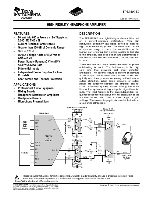
FEATURES DESCRIPTIONAPPLICATIONSFilter and I/V Gain StageStereo Hi−FiTPA6120A2SLOS431–MARCH2004HIGH FIDELITY HEADPHONE AMPLIFIER•80mW into600ΩFrom a±12-V Supply at The TPA6120A2is a high fidelity audio amplifier built0.00014%THD+N on a current-feedback architecture.This highbandwidth,extremely low noise device is ideal for •Current-Feedback Architecturehigh performance equipment.The better than120dB •Greater than120dB of Dynamic Rangeof dynamic range exceeds the capabilities of the •SNR of120dB human ear,ensuring that nothing audible is lost dueto the amplifier.The solid design and performance of •Output Voltage Noise of5µVrms atthe TPA6120A2ensures that music,not the amplifier, Gain=2V/Vis heard.•Power Supply Range:±5V to±15VThree key features make current-feedback amplifiers •1300V/µs Slew Rateoutstanding for audio.The first feature is the high •Differential Inputs slew rate that prevents odd order distortion•Independent Power Supplies for Low anomalies.The second feature is current-on-demand Crosstalk at the output that enables the amplifier to respondquickly and linearly when necessary without risk of •Short Circuit and Thermal Protectionoutput distortion.When large amounts of outputpower are suddenly needed,the amplifier can re-spond extremely quickly without raising the noise •Professional Audio Equipment floor of the system and degrading the signal-to-noise •Mixing Boards ratio.The third feature is the gain-independent fre-quency response that allows the full bandwidth of the •Headphone Distribution Amplifiersamplifier to be used over a wide range of gain •Headphone Driverssettings.The excess loop gain does not deteriorate at •Microphone Preamplifiers a rate of20dB/decade.Please be aware that an important notice concerning availability,standard warranty,and use in critical applications of TexasInstruments semiconductor products and disclaimers thereto appears at the end of this data sheet.PowerPAD is a trademark of Texas Instruments. ABSOLUTE MAXIMUM RATINGSDISSIPATION RATING TABLEAVAILABLE OPTIONSRECOMMENDED OPERATING CONDITIONSTPA6120A2SLOS431–MARCH2004These devices have limited built-in ESD protection.The leads should be shorted together or the device placed in conductive foam during storage or handling to prevent electrostatic damage.over operating free-air temperature range(unless otherwise noted)(1)(1)Stresses beyond those listed under“absolute maximum ratings”may cause permanent damageto the device.These are stress ratings only,and functional operation of the device at these or any other conditions beyond those indicated under“recommended operating conditions”is not implied.Exposure to absolute–maximum–rated conditions for extended periods may affect device reliability.(2)When the TPA6120A2is powered down,the input source voltage must be kept below600-mV peak.(3)The TPA6120A2incorporates an exposed PowerPAD on the underside of the chip.This acts as a heatsink and must be connected to athermally dissipating plane for proper powerdissipation.Failure to do so may result in exceeding the maximum junction temperature that could permanently damage the device.See TI Technical Brief SLMA002for more information about utilizing the PowerPAD thermally enhanced package.(1)The PowerPAD must be soldered to a thermal land on the printed-circuit board.See the PowerPADThermally Enhanced Package application note(SLMA002)(1)The DWP package is available taped and reeled.To order a taped and reeled part,add the suffix Rto the part number(e.g.,TPA6120A2DWPR).ELECTRICAL CHARACTERISTICSTPA6120A2 SLOS431–MARCH2004over operating free-air temperature range(unless otherwise noted)OPERATING CHARACTERISTICS (1)TPA6120A2SLOS431–MARCH 2004T A =25°C,R L =25Ω,Gain =2V/V (unless otherwise noted)(1)For IMD,THD+N,k SVR ,and crosstalk,the bandwidth of the measurement instruments was set to 80kHz.DEVICE INFORMATIONLOUT LVCC+ LIN+NCNCNCNCNC RVCC−ROUT RVCC+ RIN+ RIN−NCNCNCNCNCNC − No internal connectionTPA6120A2 SLOS431–MARCH2004Thermally Enhansed SOIC(DWP) PowerPAD™PackageTop View TERMINAL FUNCTIONSTYPICAL CHARACTERISTICSTable of Graphs101001 k10 k50 kT H D +N −T o t a l H a r m o n i c D i s t o r t i o n + N o i s e − %f − Frequency − Hz101001 k10 k50 kT H D +N −T o t a l H a r m o n i c D i s t o r t i o n + N o i s e − %f − Frequency − HzTPA6120A2SLOS431–MARCH 2004TOTAL HARMONIC DISTORTION +NOISETOTAL HARMONIC DISTORTION +NOISEvsvsFREQUENCYFREQUENCYFigure 1.Figure 2.0.00010.010.1T H D +N −T o t a l H a r m o n i c D i s t o r t i o n + N o i s e − %f − Frequency − Hz0.001T H D +N −T o t a l H a r m o n i c D i s t o r t i o n + N o i s e − %f − Frequency − Hz101001 k10 k 50 kT H D +N −T o t a l H a r m o n i c D i s t o r t i o n + N o i s e − %V O − Output Voltage − V PPT H D +N −T o t a l H a r m o n i c D i s t o r t i o n + N o i s e − %P O − Output Power − W0.000010.011100.00010.0010.1TPA6120A2SLOS431–MARCH 2004TYPICAL CHARACTERISTICS (continued)TOTAL HARMONIC DISTORTION +NOISETOTAL HARMONIC DISTORTION +NOISEvsvsFREQUENCYFREQUENCYFigure 3.Figure 4.TOTAL HARMONIC DISTORTION +NOISETOTAL HARMONIC DISTORTION +NOISEvsvsOUTPUT VOLTAGEOUTPUT POWERFigure 5.Figure 6.T H D +N −T o t a l H a r m o n i c D i s t o r t i o n + N o i s e − %0.011100.00010.0010.1P O − Output Power − WT H D +N −T o t a l H a r m o n i c D i s t o r t i o n + N o i s e − %0.011100.00010.0010.1P O − Output Power − W−90−80−70−60−50−40−30−200101001 k10 k 50 kk S V R − S u p p l y V ol t a g e R e j e c t i o n R a t i o − d Bf − Frequency − Hz−10− P o w e r D i s s i p a t i o n − WP D P O − Output Power − WTPA6120A2SLOS431–MARCH 2004TYPICAL CHARACTERISTICS (continued)TOTAL HARMONIC DISTORTION +NOISETOTAL HARMONIC DISTORTION +NOISEvsvsOUTPUT POWEROUTPUT POWERFigure 7.Figure 8.POWER DISSIPATIONSUPPLY VOLTAGE REJECTION RATIOvsvsOUTPUT POWERFREQUENCYFigure 9.Figure 10.0.0010.12 k10 k50 kI n t e r m o d u l a t i o n D i s t o r t i o n − %f − High Frequency − Hz−90−80−70−60−50−40−30−20−0101001 k10 k50 kk S V R − S u p p l y V o l t a g e R e j e c t i o n R a t i o − d Bf − Frequency − Hz−10−1C r o s s t a l k − d Bf − Frequency − HzIM Amplitude (At Input) − V PP0.000010.011100.00010.0010.1I n t e r m o d u l a t i o n D i s t o r t i o n − %TPA6120A2SLOS431–MARCH 2004TYPICAL CHARACTERISTICS (continued)SUPPLY VOLTAGE REJECTION RATIOINTERMODULATION DISTORTIONvsvsFREQUENCYHIGH FREQUENCYFigure 11.Figure 12.INTERMODULATION DISTORTIONCROSSTALKvsvsIM AMPLITUDE (AT INPUT)FREQUENCYFigure 13.Figure 14.S i g n a l −T o −N o i s e R a t i o − d BGain − V/V S i g n a l −T o −N o i s e R a t i o − dBGain − V/VOutput Step (Peak−To−Peak) − V1500100209005110070010130050030015S l e w R a t e − V /sµOutput Step (Peak−To−Peak) − V10001005700180060023900S l e w R a t e − V /sµ5003004400200TPA6120A2SLOS431–MARCH 2004TYPICAL CHARACTERISTICS (continued)SIGNAL-TO-NOISE RATIOSIGNAL-TO-NOISE RATIOvs vs GAINGAINFigure 15.Figure 16.SLEW RATESLEW RATEvsvsOUTPUT STEPOUTPUT STEPFigure 17.Figure 18.10M 100k500M1M100M 10k1k10010f − Frequency − Hz−18−15O u t p u t L e v e l − d B V−12−3−9−6−24−2110M 100k500M1M100M 10k1k10010f − Frequency − Hz−12−9O u t p u t L e v e l − d B V−63−30−18−15t − Time − ns100−1000−200V O − O u t p u t V o l t a g e − m V300200400−300−400t − Time − nsV O − O u t p u t V o l t a g e − V15010050200250350300400450500SMALL AND LARGE SIGNAL SMALL AND LARGE SIGNAL FREQUENCY RESPONSEFREQUENCY RESPONSEFigure 19.Figure 20.400-mV STEP RESPONSE10-V STEP RESPONSEFigure 21.Figure 22.t − Time − ns4−40−8V O − O u t p u t V o l t a g e − V12816−12−1620-V STEP RESPONSEFigure 23.APPLICATION INFORMATIONCurrent-Feedback AmplifiersIndependent Power SuppliesPower Supply DecouplingResistor ValuesR LV IThe TPA6120A2is a current-feedback amplifier with differential inputs and single-ended outputs.Current-feedback results in low voltage noise,high open-loop gain throughout a large frequency range,and low distortion.It can be used in a similar fashion as voltage-feedback amplifiers.The low distortion of the TPA6120A2results in a signal-to-noise ratio of 120dB as well as a dynamic range of 120dB.The TPA6120A2consists of two independent high-fidelity amplifiers.Each amplifier has its own voltage supply.This allows the user to leave one of the amplifiers off,saving power,and reducing the heat generated.It also reduces crosstalk.Although the power supplies are independent,there are some limitations.When both amplifiers are used,the same voltage must be applied to each amplifier.For example,if the left channel amplifier is connected to a ±12-V supply,the right channel amplifier must also be connected to a ±12-V supply.If it is connected to a different supply voltage,the device may not operate properly and consistently.When the use of only one amplifier is preferred,it must be the left amplifier.The voltage supply to the left amplifier is also responsible for internal start-up and bias circuitry of the device.Regardless of whether one or both amplifiers are used,the V CC-pins of both amplifiers must always be at the same potential.To power down the right channel amplifier,disconnect the V CC+pin from the power source.The two independent power supplies can be tied together on the board to receive their power from the same source.As with any design,proper power supply decoupling is essential.It prevents noise from entering the device via the power traces and provides the extra power the device can sometimes require in a rapid fashion.This prevents the device from being momentarily current starved.Both of these functions serve to reduce distortion,leaving a clean,uninterrupted signal at the output.Bulk decoupling capacitors should be used where the main power is brought to the board.Smaller capacitors should be placed as close as possible to the actual power pins of the device.Because the TPA6120A2has four power pins,use four surface mount capacitors.Both types of capacitors should be low ESR.Figure 24.Single-Ended Input With a Noninverting Gain of 2V/VIn the most basic configuration (see Figure 24),four resistors must be considered,not including the load impedance.The feedback and input resistors,R F and R I ,respectively,determine the closed-loop gain of the amplifier.R O is a series output resistor designed to protect the amplifier from any capacitance on the output path,including board and load capacitance.R S is a series input resistor.Because the TPA6120A2is a current-feedback amplifier,take care when choosing the feedback resistor.R LV IR LV V I+The value of the feedback resistor should be chosen by using Figure 27through Figure 32as guidelines.The gain can then be set by adjusting the input resistor.The smaller the feedback resistor,the less noise is introduced into the system.However,smaller values move the dominant pole to higher and higher frequencies,making the device more susceptible to oscillations.Higher feedback resistor values add more noise to the system,but pull the dominant pole down to lower frequencies,making the device more stable.Higher impedance loads tend to make the device more unstable.One way to combat this problem is to increase the value of the feedback resistor.It is not recommended that the feedback resistor exceed a value of 10k Ω.The typical value for the feedback resistor for the TPA6120A2is 1k Ω.In some cases,where a high-impedance load is used along with a relatively large gain and a capacitive load,it may be necessary to increase the value of the feedback resistor from 1k Ωto 2k Ω,thus adding more stability to the system.Another method to deal with oscillations is to increase the size of R O .CAUTION:Do not place a capacitor in the feedback path.Doing so can cause oscillations.Capacitance at the outputs can cause oscillations.Capacitance from some sources,such as layout,can be minimized.Other sources,such as those from the load (e.g.,the inherent capacitance in a pair of headphones),cannot be easily minimized.In this case,adjustments to R O and/or R F may be necessary.The series output resistor should be kept at a minimum of 10Ω.It is small enough so that the effect on the load is minimal,but large enough to provide the protection necessary such that the output of the amplifier sees little capacitance.The value can be increased to provide further isolation,up to 100Ω.The series resistor,R S ,should be used for two reasons:1.It prevents the positive input pin from being exposed to capacitance from the line and source.2.It prevents the source from seeing the input capacitance of the TPA6120A2.The 50-Ωresistor was chosen because it provides ample protection without interfering in any noticeable way with the signal.Not shown is another 50-Ωresistor that can be placed on the source side of R S to ground.In that capacity,it serves as an impedance match to any 50-Ωsource.Figure 25.Single-Ended Input With a Noninverting Gain of -1V/VFigure 26.Differential Input With a Noninverting Gain of 2V/VFigure 26shows the TPA6120A2connected with differential inputs.Differential inputs are useful because they take the greatest advantage of the device's high CMRR.The two feedback resistor values must be kept the same,as do the input resistor values.Checking for Oscillations and Instabilityf − Frequency − Hzf − Frequency − HzSpecial note regarding mono operation:•If both amplifiers are powered on,but only one channel is to be used,the unused amplifier MUST have afeedback resistor from the output to the negative input.Additionally,the positive input should be grounded as close to the pin as possible.Terminate the output as close to the output pin as possible with a 25-Ωload to ground.•These measures should be followed to prevent the unused amplifier from oscillating.If it oscillates,and thepower pins of both amplifiers are tied together,the performance of the amplifier could be seriously degraded.Checking the stability of the amplifier setup is recommended.High frequency oscillations in the megahertz region can cause undesirable effects in the audio band.Sometimes,the oscillations can be quite clear.An unexpectedly large draw from the power supply may be an indication of oscillations.These oscillations can be seen with an oscilloscope.However,if the oscillations are not obvious,or there is a chance that the system is stable but close to the edge,placing a scope probe with 10pF of capacitance can make the oscillations worse,or actually cause them to start.A network analyzer can be used to determine the inherent stability of a system.An output vs frequency curve generated by a network analyzer can be a good indicator of stability.At high frequencies,the curve shows whether a system is oscillating,close to oscillation,or stable.Looking at Figure 27through Figure 32,several different phenomena occur.In one scenario,the system is stable because the high frequency rolloff is smooth and has no peaking.Increasing R F decreases the frequency at which this rolloff occurs (see the Resistor Values section).Another scenario shows some peaking at high frequency.If the peaking is 2dB,the amplifier is stable as there is still 45degrees of phase margin.As the peaking increases,the phase margin shrinks,the amplifier and the system,move closer to instability.The same system that has a 2-dB peak has an increased peak when a capacitor is added to the output.This indicates the system is either on the verge of oscillation or is oscillating,and corrective action is required.Figure 27.Normalized Output Response vs Frequency Figure 28.Normalized Output Response vs Frequencyf − Frequency − Hz N o r m a l i z e d O u t p u t R e s p o n s e − d B110M 100k500M1M 100M 10k1k10010f − Frequency − HzN o r m a l i z e d O u t p u t R e s p o n s e − d B110M 100k 500M 1M 100M 10k 1k10010f − Frequency − HzO u t p u t A m p l i t u d e − d B031210M 100k 500M 1M 100M 10k 1k10010f − Frequency − HzO u t p u t A m p l i t u d e − d BPCB LayoutFigure 29.Normalized Output Response vs FrequencyFigure 30.Normalized Output Response vs FrequencyFigure 31.Output Amplitude vs Frequency Figure 32.Output Amplitude vs FrequencyProper board layout is crucial to getting the maximum performance out of the TPA6120A2.A ground plane should be used on the board to provide a low inductive ground connection.Having a ground plane underneath traces adds capacitance,so care must be taken when laying out the ground plane on the underside of the board (assuming a 2-layer board).The ground plane is necessary on the bottom for thermal reasons.However,certain areas of the ground plane should be left unfilled.The area underneath the device where the PowerPAD is soldered down should remain,but there should be no ground plane underneath any of the input and output pins.This places capacitance directly on those pins and leads to oscillation problems.The underside ground plane should remain unfilled until it crosses the device side of the input resistors and the output series resistor.Thermal reliefs should be avoided if possible because of the inductance they introduce.R OR LVR L Thermal ConsiderationsEfficiency of an amplifier+P LP SUP(1)P L+V LRMS2R L,and V LRMS+V P2Ǹ,therefore,P L+V P22R Lper channel(2)P SUP+V CC I CC avg)V CC I CC(q)(3)I CC avg+1pŕp 20V PR Lsin(t)dt+*V Pp RL[cos(t)]p2+V Pp RL(4)Despite the removal of the ground plane in critical areas,stray capacitance can still make its way onto the sensitive outputs and inputs.Place components as close as possible to the pins and reduce trace lengths.See Figure33and Figure34.It is important for the feedback resistor to be extremely close to the pins,as well as the series output resistor.The input resistor should also be placed close to the pin.If the amplifier is to be driven in a noninverting configuration,ground the input close to the device so the current has a short,straight path to the PowerPAD(gnd).yout That Can Cause Oscillationyout Designed To Reduce Capacitance On Critical NodesAmplifiers can generate quite a bit of heat.Linear amplifiers,as opposed to Class-D amplifiers,are extremely inefficient,and heat dissipation can be a problem.There is no one to one relationship between output power and heat dissipation,so the following equations must be used:WhereWhereV P +2P L R LǸ(5)P SUP +V CC VP p R L)V CC I CC(q)(6)P DISS +(1*h )P SUP(7)T A Max +T J Max *ΘJA P Diss(8)− P o w e r D i s s i p a t i o n − WP DP O − Output Power − WTherefore,P L =Power delivered to load (per channel)P SUP =Power drawn from power supply V LRMS =RMS voltage on the load R L =Load resistanceV P =Peak voltage on the loadI CC avg =Average current drawn from the power supply I CC (q)=Quiescent current (per channel)V CC =Power supply voltage (total supply voltage =30V if running on a ±15-V power supply η=Efficiency of a SE amplifierFor stereo operation,the efficiency does not change because both P L and P SUP are doubled.This effects the amount of power dissipated by the package in the form of heat.A simple formula for calculating the power dissipated,P DISS ,is shown in Equation 7:In stereo operation,P SUP is twice the quantity that is present in mono operation.The maximum ambient temperature,T A ,depends on the heat-sinking ability of the system.θJA for a 20-pin DWP,whose thermal pad is properly soldered down,is shown in the dissipation rating table.Figure 35.Power Dissipation vs Output PowerApplication Circuit10 µF5 V µF−5 V OPA413412 V µFTPA6120A2Figure 36.Typical Application CircuitIn many applications,the audio source is digital.It must go through a digital-to-analog converter (DAC)so that traditional analog amplifiers can drive the speakers or headphones.Figure 36shows a complete circuit schematic for such a system.The digital audio is fed into a high performance DAC.The PCM1792,a Burr-Brown product from TI,is a 24-bit,stereo DAC.The output of the PCM1792is current,not voltage,so the OPA4134is used to convert the current input to a voltage output.The OPA4134,a Burr-Brown product from TI,is a low-noise,high-speed,high-performance operational amplifier.C F and R F are used to set the cutoff frequency of the filter.The RC combination in Figure 36has a cutoff frequency of 59kHz.All four amplifiers of the OPA4134are used so the TPA6120A2can be driven differentially.The output of the OPA4134goes into the TPA6120A2.The TPA6120A2is configured for use with differential inputs,stereo use,and a gain of2V/V.Note that the0.1-uF capacitors are placed at every supply pin of the TPA6120A2,as well as the10-Ωseries output resistor.Each output goes to one channel of a pair of stereo headphones,where the listener enjoys crisp,clean,virtually noise free music with a dynamic range greater than the human ear is capable of detecting.PACKAGING INFORMATION Orderable DeviceStatus (1)Package Type Package Drawing Pins Package Qty Eco Plan (2)Lead/Ball Finish MSL Peak Temp (3)TPA6120A2DWP ACTIVE SOPowerPADDWP 2025Green (RoHS &no Sb/Br)CU NIPDAU Level-2-260C-1YEAR TPA6120A2DWPG4ACTIVE SOPowerPADDWP 2025Green (RoHS &no Sb/Br)CU NIPDAU Level-2-260C-1YEAR TPA6120A2DWPR ACTIVE SOPowerPADDWP 202000Green (RoHS &no Sb/Br)CU NIPDAU Level-2-260C-1YEAR TPA6120A2DWPRG4ACTIVE SOPowerPAD DWP 202000Green (RoHS &no Sb/Br)CU NIPDAU Level-2-260C-1YEAR(1)The marketing status values are defined as follows:ACTIVE:Product device recommended for new designs.LIFEBUY:TI has announced that the device will be discontinued,and a lifetime-buy period is in effect.NRND:Not recommended for new designs.Device is in production to support existing customers,but TI does not recommend using this part in a new design.PREVIEW:Device has been announced but is not in production.Samples may or may not be available.OBSOLETE:TI has discontinued the production of the device.(2)Eco Plan -The planned eco-friendly classification:Pb-Free (RoHS),Pb-Free (RoHS Exempt),or Green (RoHS &no Sb/Br)-please check /productcontent for the latest availability information and additional product content details.TBD:The Pb-Free/Green conversion plan has not been defined.Pb-Free (RoHS):TI's terms "Lead-Free"or "Pb-Free"mean semiconductor products that are compatible with the current RoHS requirements for all 6substances,including the requirement that lead not exceed 0.1%by weight in homogeneous materials.Where designed to be soldered at high temperatures,TI Pb-Free products are suitable for use in specified lead-free processes.Pb-Free (RoHS Exempt):This component has a RoHS exemption for either 1)lead-based flip-chip solder bumps used between the die and package,or 2)lead-based die adhesive used between the die and leadframe.The component is otherwise considered Pb-Free (RoHS compatible)as defined above.Green (RoHS &no Sb/Br):TI defines "Green"to mean Pb-Free (RoHS compatible),and free of Bromine (Br)and Antimony (Sb)based flame retardants (Br or Sb do not exceed 0.1%by weight in homogeneous material)(3)MSL,Peak Temp.--The Moisture Sensitivity Level rating according to the JEDEC industry standard classifications,and peak solder temperature.Important Information and Disclaimer:The information provided on this page represents TI's knowledge and belief asof the date that it is provided.TI bases its knowledge and belief on information provided by third parties,and makes no representation or warranty as to the accuracy of such information.Efforts are underway to better integrate information from third parties.TI has taken and continues to take reasonable steps to provide representative and accurate information but may not have conducted destructive testing or chemical analysis on incoming materials and chemicals.TI and TI suppliers consider certain information to be proprietary,and thus CAS numbers and other limited information may not be available for release.In no event shall TI's liability arising out of such information exceed the total purchase price of the TI part(s)at issue in this document sold by TI to Customer on an annual basis.PACKAGE OPTION ADDENDUM 5-Oct-2007Addendum-Page 1IMPORTANT NOTICETexas Instruments Incorporated and its subsidiaries(TI)reserve the right to make corrections,modifications,enhancements,improvements, and other changes to its products and services at any time and to discontinue any product or service without notice.Customers should obtain the latest relevant information before placing orders and should verify that such information is current and complete.All products are sold subject to TI’s terms and conditions of sale supplied at the time of order acknowledgment.TI warrants performance of its hardware products to the specifications applicable at the time of sale in accordance with TI’s standard warranty.Testing and other quality control techniques are used to the extent TI deems necessary to support this warranty.Except where mandated by government requirements,testing of all parameters of each product is not necessarily performed.TI assumes no liability for applications assistance or customer product design.Customers are responsible for their products and applications using TI components.To minimize the risks associated with customer products and applications,customers should provide adequate design and operating safeguards.TI does not warrant or represent that any license,either express or implied,is granted under any TI patent right,copyright,mask work right, or other TI intellectual property right relating to any combination,machine,or process in which TI products or services are rmation published by TI regarding third-party products or services does not constitute a license from TI to use such products or services or a warranty or endorsement e of such information may require a license from a third party under the patents or other intellectual property of the third party,or a license from TI under the patents or other intellectual property of TI.Reproduction of TI information in TI data books or data sheets is permissible only if reproduction is without alteration and is accompanied by all associated warranties,conditions,limitations,and notices.Reproduction of this information with alteration is an unfair and deceptive business practice.TI is not responsible or liable for such altered rmation of third parties may be subject to additional restrictions.Resale of TI products or services with statements different from or beyond the parameters stated by TI for that product or service voids all express and any implied warranties for the associated TI product or service and is an unfair and deceptive business practice.TI is not responsible or liable for any such statements.TI products are not authorized for use in safety-critical applications(such as life support)where a failure of the TI product would reasonably be expected to cause severe personal injury or death,unless officers of the parties have executed an agreement specifically governing such use.Buyers represent that they have all necessary expertise in the safety and regulatory ramifications of their applications,and acknowledge and agree that they are solely responsible for all legal,regulatory and safety-related requirements concerning their products and any use of TI products in such safety-critical applications,notwithstanding any applications-related information or support that may be provided by TI.Further,Buyers must fully indemnify TI and its representatives against any damages arising out of the use of TI products in such safety-critical applications.TI products are neither designed nor intended for use in military/aerospace applications or environments unless the TI products are specifically designated by TI as military-grade or"enhanced plastic."Only products designated by TI as military-grade meet military specifications.Buyers acknowledge and agree that any such use of TI products which TI has not designated as military-grade is solely at the Buyer's risk,and that they are solely responsible for compliance with all legal and regulatory requirements in connection with such use. TI products are neither designed nor intended for use in automotive applications or environments unless the specific TI products are designated by TI as compliant with ISO/TS16949requirements.Buyers acknowledge and agree that,if they use any non-designated products in automotive applications,TI will not be responsible for any failure to meet such requirements.Following are URLs where you can obtain information on other Texas Instruments products and application solutions:Products ApplicationsAmplifiers Audio /audioData Converters Automotive /automotiveDLP®Products Communications and /communicationsTelecomDSP Computers and /computersPeripheralsClocks and Timers /clocks Consumer Electronics /consumer-appsInterface Energy /energyLogic Industrial /industrialPower Mgmt Medical /medicalMicrocontrollers Security /securityRFID Space,Avionics&/space-avionics-defenseDefenseRF/IF and ZigBee®Solutions /lprf Video and Imaging /videoWireless /wireless-appsMailing Address:Texas Instruments,Post Office Box655303,Dallas,Texas75265Copyright©2010,Texas Instruments Incorporated。
马克320s前级说明书
马克320s前级说明书第一章:产品概述马克320s前级是一款高性能音频前置放大器,专为提升音频信号的放大效果而设计。
该前级采用了先进的技术,具备出色的音频放大功能,能够提供清晰、准确、动态的音频输出。
马克320s前级适用于各类音频设备的升级和扩展,能够显著提升音频系统的性能和音质。
第二章:产品特点1.高性能放大器芯片:马克320s前级采用了高性能的放大器芯片,具备低噪声、高增益和高线性的特点,能够有效地放大音频信号,提供更加真实和细腻的音质体验。
2.精心调校的音频电路:马克320s前级经过精心调校,采用了优质的电子元件,确保音频信号的传输和放大过程中能够最大限度地减少失真和干扰,提供高保真的音频输出。
3.灵活的输入输出接口:马克320s前级配备了多种输入输出接口,支持多种音频设备的连接,能够满足不同用户的需求。
4.人性化的设计:马克320s前级采用了简约而优雅的外观设计,配备了直观易用的操作面板和显示屏,用户可以方便地调节音频参数和监控工作状态。
第三章:产品规格1.输入阻抗:10kΩ2.输出阻抗:100Ω3.最大输出电压:2V4.频率响应:20Hz-20kHz5.信噪比:>100dB6.失真率:<0.01%7.电源要求:AC 220V,50Hz8.功耗:30W9.尺寸:430mm × 80mm × 320mm10.重量:5kg第四章:使用方法1.将音频源设备与马克320s前级的输入接口连接,确保连接牢固。
2.将马克320s前级的输出接口与音频功放或扬声器连接,确保连接牢固。
3.打开音频源设备和马克320s前级的电源开关。
4.调节马克320s前级的音量控制旋钮,使音频输出达到适合的音量。
5.根据需要,调节马克320s前级的音频参数,如低音、高音等,以获得最佳的音质效果。
第五章:常见问题解答1.马克320s前级是否支持蓝牙连接?不支持,马克320s前级只能通过有线连接与音频源设备进行连接。
- 1、下载文档前请自行甄别文档内容的完整性,平台不提供额外的编辑、内容补充、找答案等附加服务。
- 2、"仅部分预览"的文档,不可在线预览部分如存在完整性等问题,可反馈申请退款(可完整预览的文档不适用该条件!)。
- 3、如文档侵犯您的权益,请联系客服反馈,我们会尽快为您处理(人工客服工作时间:9:00-18:30)。
第一章高性能(特殊)运算放大器内容:一.集成运算放大器的主要参数二.动态校零型斩波放大器三.仪器放大器四.隔离放大器五.仪器放大器和隔离放大器的应用引言问题1:放大器的作用?等效模型?有哪几个参数?问题2:运放的基本结构?多级直接耦合放大电路存在的主要问题?为何采用差分输入级?放大电路的等效模型:主要有Ri,Ro和Avo三个参数。
还有其它一些参数如:带宽等。
集成电路运算放大器是一种①高电压增益、②高输入阻抗和③低输出阻抗的④多级直接耦合放大电路。
它的类型很多,电路也不一样,但结构具有共同之处。
图1-1是集成运故的内部电路组成原理框图,图1-2是uA741的内部电路图。
(1)图中输入级一般是由BJT,JFET或MOSFET组成的差分式放大电路,利用它的对称特性可以提高整个电路的共模抑制比和抑制零点漂移,它的两个输入端构成整个电路的反相输入端和同相输入端。
(2)电压放大级的主要作用是提高电压增益,它可由一级或多级直接耦合放大电路组成。
(3)输出级一般由电压跟随器或互补电压跟随器所组成,以降低输出电阻,提高带负载能力。
(4)偏置电路是为各级提供合适的工作电流。
此外还有一些辅助环节,如电平移动电路、过载保护电路以及高频补偿环节等。
复习:运算放大器理想化模型所做的几点假设是什么?(1)(2)(3)(4)复习:理想运放在负反馈电路中有哪两个特点?问题1:反相比例放大器的电路, 放大倍数,反馈类型和特点,电路特点?问题2:同相比例放大器的电路, 放大倍数,反馈类型和特点,电路特点?问题3:一个实际使用时的有趣问题:下图中输出电压Vo=?理想运放假设:虚短、虚断为了正确地挑选和使用集成运放,必须搞清它的参数的含义!运放的分类也是根据参数的不同划分的。
第一节集成运算放大器的主要参数集成运算放大器的应用从最初的信号运算发展到现在几乎应用于电子技术的各个领域。
因此熟练掌握集成运放电路的分析和设计方法,是在实际工作中灵活应用运算放大器的重要基础。
1.1 运算放大器的参数和型号1.1.1 运算放大器的参数运算放大器的技术参数很多,其中部分指标与差分放大器和功率放大器相同,另一部分指标是根据运算放大器本身的特点而设立的。
通用型运算放大器的各种参数均比较适中,特殊运算放大器的某些技术指标很高,如:高精度,高速,低噪声和高输入阻抗等。
运算放大器参数分为两大类:静态(DC)技术指标运算放大器的静态技术指标包括:(1)输入失调电压V IO一个理想的集成运故,当输入电压为零时,输出电压也应为零(不加调零装置)。
但实际上它的差分输入级很难做到完全对称,通常在输入电压为零时,存在一定的输出电压。
在室温(25℃)及标准电源电压下,输入电压为零时,为了使集成运放的输出电压为零,在输入端加的补偿电压叫做失调电压Vio。
实际上指输入电压Vi=0时,输出电压Vo折合到输入端的电压的负值,即V IO=-(Vo| Vi=0)/Avo。
V IO 的大小反应了运放制造中电路的对称程度和电位配合情况。
V IO值愈大,说明电路的对称程度愈差,一般约为土(1~10)mv。
通用运放的数量级在±1mV~几十mV之间,精密(低漂移)运放的V IO在1μV~几十μV之间。
两种理解:(1)输出折算到输入;(2)输入加补偿电压!(2)输入偏置电流I IB(I IP,I IN)(对BJT有效,对FET无效)BJT集成运放的两个输入端是差分对管的基极,因此两个输入端总需要一定的输入电流I BN和I BP。
输入偏置电流是指集成运放输出电压为零时,两个输入端静态电流的平均值,如图所示。
当Vo=0时,偏置电流为输入偏置电流的大小,在电路外接电阻确定之后,主要取决于运故差分输入级BJT的性能,当它的β值太小时、将引起偏置电流增加。
从使用角度来看,偏置电流愈小,由于信号源内阻变化引起的输山电压变化也愈小,故它是重要的技术指标。
一般为10 nA~1μA。
(3)输入失调电流I IO在BJT集成电路运放中,输入失调电流I IO是指当输出电压为零时流入放大器两输入端的静态基极电流之差,即由于信号源内阻的存在,I IO会引起一输入电压,破坏放大器的平衡,使放大器输出电压不为零。
所以,希望I IO愈小愈好,它反映了输入级差分对管的不对称程度。
I IO愈小,输入级差分对管的对称程度越好,一般约为±(1nA~0.1µA)(I BN和I BP相差1%左右)。
一般约为1nA~0.1μA。
注意:输入失调电压V IO和输入失调电流I IO对放大造成的误差可以通过外接调零装置来补偿。
放大器的温度漂移是造成误差的主要来源,而它又是由输入失调电压和输入失调电流随温度的漂移所引起的。
(4)输入失调电压温漂ΔV IO/ΔT输入失调电压温漂是指在规定工作温度范围内,输入失调电压随温度的变化量与温度变化量的比值。
它是衡量电路温漂的重要指标,不能用外接调零装置的办法来补偿。
输入失调电压温漂越小越好。
通用运放的输入失调电压温漂在±(10~20)μV/℃之间,精密运放在±0.5μV/℃左右。
(5)输入失调电流温漂ΔI IO/ΔT在规定工作温度范围内,输入失调电流随温度的变化量与温度变化量之比值称为输入失调电流温漂。
输入失调电流温漂是放大电路电流漂移的量度,不能用外接调零装置来补偿。
高质量的运放每度变化几个pA/℃。
差模和共模信号的定义(图):(6)最大差模输入电压V idmax最大差模输入电压V idmax是指运放两输入端能承受的最大差模输入电压。
超过此电压,运放输入级对管将进入非线性区,而使运放的性能显著恶化,甚至造成损坏。
利用平面工艺制成的NPN管约为±5V 左右,而横向BJT可达±30V以上(7)最大共模输入电压V icmax动态(AC)技术指标运算放大器的动态技术指标包括:(8)开环差模电压放大倍数A VO开环差模电压放大倍数A Vd是指集成运放工作在线性区、接入规定的负载,输出电压的变化量与运放输入端口处的输入电压的变化量之比。
运放的A Vd在60~120dB之间。
不同功能的运放,A Vd相差悬殊。
A VO与输出电压Vo的大小有关。
通常是在规定的输出电压幅度(如Vo=土10v)测得的值。
A VO又是频率的函数,频率高于某一数值后,A VO的数值开始下降。
下图表示741型运放A VO的频率响应。
(9)开环共模电压放大倍数A CMA CM =Vocm /Vicm <<1(10)共模抑制比CMRR(Common-Mode Rejection Ratio)运放共模抑制比CMRR的定义与差分放大电路中的定义相同,是差模电压放大倍数与共模电压放大倍数之比,常用分贝数来表示。
不同功能的运放,CMRR也不相同,有的在60~70dB之间,有的高达180dB。
CMRR越大,对共模干扰抑制能力越强。
CMRR=A Vd / A CM(11)差模输入电阻Rd/共模输入电阻Rc差模输入电阻Rd是指输入差模信号时运放的输入电阻。
Rd越大,对信号源的影响越小,运放的Rd一般都在几百千欧以上。
BJT的较小、MOSFET很大!(12)开环带宽BW开环带宽又称-3dB带宽,是指运算放大器的差模电压放大倍数A Vd在高频段下降3dB所对应的频率f H。
(13)单位增益带宽BW G (f T)单位增益带宽BW G是指信号频率增加,使A Vd下降到1时所对应的频率f T,即A Vd为0dB时的信号频率f T。
它是集成运放的重要参数。
741型运放的f T=7Hz,是比较低的。
(14)转换速率S R (压摆率)转换速率S R是指放大电路在闭环状态下,输入大信号(例如阶跃信号)时,放大电路输出电压对时间的最大变化速率,见图1-1-1。
它反映了运放对于快速变化的输入信号的响应能力。
转换速率S R的表达式为转换速率S R是在大信号和高频信号工作时的一项重要指标,目前一般通用型运放压摆率在1~10V/µs左右。
图?压摆率示意图问题:下面是什么电路?放大倍数=?R2的作用是什么?如何取值?外部电阻匹配问题:问题:下面是什么电路?放大倍数=?如何加匹配电阻和取值?问题:下面是什么电路?放大倍数=?如何加匹配电阻和取值?问题:下面是什么电路?放大倍数=?如何加匹配电阻和取值?1.1.2 运算放大器的符号和型号(1) 运算放大器的符号运算放大器的符号中有三个引线端:两个输入端和一个输出端。
其中一个输入端称为同相输入端,该端输入信号与输出端输出信号的极性相同,用符号‘+’或‘IN+’表示;另一个输入端称为反相输入端,该端输入信号与输出端输出信号变化的极性相异,用符号‘-’或‘IN-’表示。
输出端一般画在输入端的另一侧,在符号边框内标有‘+’号。
实际的运算放大器还必须有正、负电源端,还可能有补偿端和调零端。
在简化电路中,电源端、调零端等都不画。
下面给出国家标准的运算放大器符号:(2) 集成运算放大器的型号命名数字序号,一般与同类型的世界上其它厂家的产品序号相同。
运算放大器功率放大器1.1.3 运算放大器分类为满足实际使用中对集成运放性能的特殊要求,除性能指标比较适中的通用型运放外,出现了适应不同需要的专用型集成运放。
根据运算放大器的技术指标可以对其进行分类,主要有:通用型高速型和宽带型高精度、低漂移型高输入电阻型低功耗型功率型1.1.3.1 通用型通用型运算放大器的技术指标比较适中,价格低廉。
通用型运放也经过了几代的演变,早期的通用Ⅰ型运放已很少使用了。
以典型的通用型运放CF741(μA741)为例,输入失调电压1~2mV、输入失调电流20nA、差模输入电阻2MΩ,开环增益100dB、共模抑制比90dB、输出电阻75Ω、共模输入电压范围±13V、转换速率0.5V/μs。
1.1.3.2 高速型和宽带型高速型和宽带型运算放大器一般用于宽频带放大器、快速A/D和D/A转换器、有源滤波器、高速取样-保持电路、锁相环、精密比较器和视频放大器中。
这种运放的单位增益带宽和压摆率的指标均较高,转换速率S R>30V/μS,单位增益带宽BW G>10MHz。
用于小信号放大时,比较注重BW G;用于高速大信号放大时,同时还应注重S R。
例如:CF2520/2525AD96181.1.3.3 高精度、低漂移型高精度、低漂移型运放,一般用于毫伏量级或更微弱信号的精密检测、精密计算、精密传感器信号变送器、高精度稳压电源及自动控制仪表中。
例如:1.1.3.4 高输入阻抗型目前, 高输入阻抗型运放广泛用于生物医学电信号测量的精密放大电路、有源滤波器、取样-保持放大器、对数和反对数放大器和模数、数模转换器等。
这种类型集成运放的差模输入电阻r id>(109~1012)Ω,输入偏置电流I IB为几皮安~几十皮安,故又称为低输入偏置电流型运放。