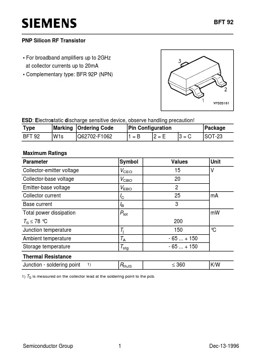
Q62702-P946中文资料
Q62702-F1062中文资料
Gma
IC = 15 mA, VCE = 8 V, ZS = ZSopt ZL = ZLopt f = 900 MHz f = 1.8 GHz
Transducer gain |S21e|2 11.5 6 13.5 8 -
IC = 15 mA, VCE = 8 V, ZS =ZL= 50 Ω f = 900 MHz f = 1.8 GHz
Package Equivalent Circuit: LBI = LBO = LEI = LEO = LCI = LCO = CBE = CCB = CCE = 84 165 0.85 0.51 0.69 0.61 0 0.49 nH nH nH nH nH nH fF fF fF
Valid up to 6 GHz For examples and ready to use parameters please contact your local Siemens distributor or sales office to obtain a Siemens CD-ROM or see Internet: http://www.siemens.de/Semiconductor/products/35/35.htm
0.90551 12.196 1.2703 0.79584 0.66749 0.32167 0.21451 922.07 0.3 0.75 1.11 300
fA mA Ω V fF V eV K
0.016123 A 0.019729 A
0.024709 fA
0.013277 mA
All parameters are ready to use, no scalling is necessary. Extracted on behalf of SIEMENS Small Signal Semiconductors by: Institut für Mobil-und Satellitenfunktechnik (IMST) © 1996 SIEMENS AG
Q62702-F1590中文资料

Maximum Ratings Parameter Collector-emitter voltage Collector-base voltage Emitter-base voltage Collector current Base current Total power dissipation, T S ≤ 96 °C Junction temperature Ambient temperature Storage temperature Thermal Resistance Junction - soldering point
Unit max. 6.5 600 100 150 V nA µA -
typ. 5 80
V(BR)CEO I CBO I EBO hFE
4.5 50
fT
15 24 17 0.48 1.33 1.75 1.25 0.75 1.6
GHz
Ccb Cce Ceb F
pF
dB
Gma
-
14
-
dB
|S21|2
8
11
Ga 1)
dB
Γopt
MAG ANG
RN
Ω
rn
-
F50Ω 2)
dB
|S21|2 2)
dB
V CE = 2V, I C = 10mA
0.9 1.8 2.4 3 4 0.9 1.25 1.45 1.7 2.1 15.5 11.8 10.9 8.5 6.6 0.29 0.47 0.56 0.62 0.66 175 -171 -159 -147 -127 2.7 3 3.5 5.5 15.5 0.054 0.06 0.07 0.11 0.31 0.98 1.74 2.23 3.05 4.49 16 9.5 6.8 4.7 1.9
SFH203中文资料

TCV
–2.6
–2.6
mV/K
TCI
%/K
0.18
–
–
0.2
NEP
2.9 x 10⁻¹⁴ 2.9 x 10⁻¹⁴
W
√Hz
D*
3.5 x 10¹² 3.5 x 1012 cm · √Hz
W
Semiconductor Group
Photocurrent IP = f (Ee), VR = 5 V Open-circuit-voltage VL= f (Ee) SFH 2030 F
Total power dissipation Ptot = f (TA)
Dark current IR characteristics Srel = f (ϕ)
Spektraler Bereich der Fotoempfindlichkeit S = 10% von Smax Spectral range of sensitivity S = 10% of Smax Bestrahlungsempfindliche Fläche Radiant sensitive area
VF
Forward voltage
420 (≥ 350) –
mV
–
370 (≥ 300) mV
80
–
µA
–
25
µA
5
5
ns
1.3
1.3
V
Kapazität, VR = 0 V, f = 1 MHz, E = 0
C0
11
11
pF
Capacitance
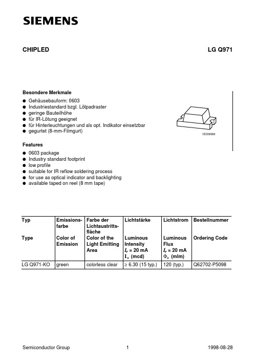
LGQ971中文资料
Stoßstrom Surge current
tp ≤ 10 µs, D = 0.005
Sperrspanung Reverse voltage
Verlustleistung Power dissipation
Wärmewiderstand Sperrschicht / Umgebung Thermal resistance Junction / air
Standard eye response curve
1.0
% Ι rel
0.8 Vλ
0.7
0.6
0.5
0.4
0.3
0.2
0.1
0
400
450
500
550
600
650
Abstrahlcharakteristik Irel = f (ϕ)
Radiation characteristic
40˚
30˚
20˚
Temperaturkoeffizient von VF, IF = 20 mA (typ.) Temperature coefficient of VF, IF = 20 mA (typ.)
Temperaturkoeffizient von IV, IF = 20 mA (typ.) Temperature coefficient of IV, IF = 20 mA (typ.)
Temperaturkoeffizient von λpeak, IF = 20 mA Temperature coefficient of λpeak, IF = 20 mA
(typ.) (typ.)
Temperaturkoeffizient von ∆λ (IF = 20 mA) Temperature coefficient of ∆λ (IF = 20 mA)
SFH757中文资料
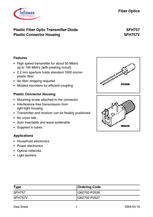
Type Ordering Code SFH757Q62702-P3526SFH757VQ62702-P3527Plastic Fiber Optic Transmitter Diode Plastic Connector HousingSFH757SFH757VFiber OpticsFeatures•High speed transmitter for about 50Mbit/s up to 100Mbit/s (with peaking circuit)• 2.2mm aperture holds standard 1000 micron plastic fiber•No fiber stripping required•Molded microlens for efficient coupling Plastic Connector Housing•Mounting screw attached to the connector •Interference-free transmission from light-tight housing•Transmitter and receiver can be flexibly positioned •No cross talk•Auto insertable and wave solderable •Supplied in tubes Applications •Household electronics •Power electronics •Optical networks •LightbarriersTechnical DataAbsolute Maximum RatingsParameter Symbol Limit Values Unitmin.max. Operating Temperature Range T OP–40+80°C Storage Temperature Range T STG–40+100°C Junction Temperature T J100°CSoldering Temperature(2mm from case bottom, t≤ 5s)TS260°CReverse Voltage V R3V Forward Current I F50mA Surge Current (t≤ 10µs, D=0)I FSM1A Power Dissipation P tot120mW Thermal Resistance, Junction/Air R thJA450K/WCharacteristics (T A = 25°C)Parameter Symbol Value Unit Peak WavelengthλPeak650nm Spectral Bandwidth∆λ25nmSwitching Times (R L = 50Ω, I F = 50mA) 10% …90%90% … 10%tRtF15 (< 17)18 (< 20)nsCapacitance (f = 1MHz, V R = 0V)C O30pF Forward Voltage (I F = 50mA)V F 2.1 (≤ 2.8)VOutput Power Coupled into Plastic Fiber (I F = 10mA)1)ΦIN150(≥ 100)µWTemperature Coefficient ΦIN TCΦ–0.4%/K Temperature Coefficient V F TC V–3mV/K Temperature Coefficient λPeak TCλ0.16nm/K1)The output power coupled into plastic fiber is measured with a large area detector at the end of a short lengthof fiber (about 30cm). This value must not be used for calculating the power budget for a fiber optic system with a long fiber because the numerical aperture of plastic fibers decreases on the first meters. Therefore the fiber seems to have a higher attenuation over the first few meters compared with the specified value.Relative Spectral Emission I rel = f (λ)Relative Output Power I e /I e(50 mA) = f (I F ) single pulse, duration = 20 µsForward Current I F = f (V F ) single pulse, duration = 20 µsMaximum Permissible Forward Current IF = f (T A ), R thJA= 450 K/WPermissible Pulse Handling CapabilityI F = f(t P), duty cycle D = parameter,TA= 25°CSFH757SFH757VPackage Outlines Package OutlinesFigure1Figure2Edition 2004-03-19Published by Infineon Technologies AG,St.-Martin-Strasse 53,81669 München, Germany© Infineon Technologies AG 2004.All Rights Reserved.Attention please!The information herein is given to describe certain components and shall not be considered as a guarantee of characteristics.Terms of delivery and rights to technical change reserved.We hereby disclaim any and all warranties, including but not limited to warranties of non-infringement, regarding circuits, descriptions and charts stated rmationFor further information on technology, delivery terms and conditions and prices please contact your nearest Infineon Technologies Office ( ).WarningsDue to technical requirements components may contain dangerous substances. For information on the types in question please contact your nearest Infineon Technologies Office.Infineon Technologies Components may only be used in life-support devices or systems with the express written approval of Infineon Technologies, if a failure of such components can reasonably be expected to cause the failure of that life-support device or system, or to affect the safety or effectiveness of that device or system. Life support devices or systems are intended to be implanted in the human body, or to support and/or maintain and sustain and/or protect human life. If they fail, it is reasonable to assume that the health of the user or other persons may SFH757SFH757V Revision History:2004-03-19DS1Previous Version:2002-03-14。
SFH3010中文资料
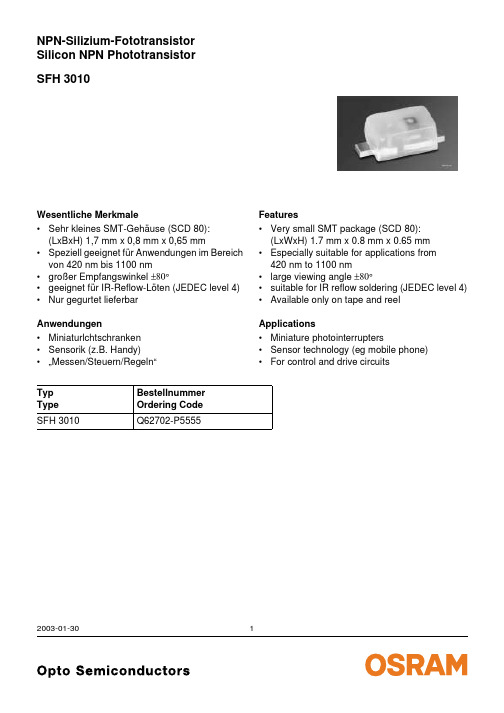
SFH 3010NPN-Silizium-FototransistorSilicon NPN Phototransistor 2003-01-301Wesentliche Merkmale•Sehr kleines SMT-Gehäuse (SCD 80):(LxBxH) 1,7 mm x 0,8 mm x 0,65 mm•Speziell geeignet für Anwendungen im Bereich von 420nm bis 1100nm •großer Empfangswinkel ±80°•geeignet für IR-Reflow-Löten (JEDEC level 4)•Nur gegurtet lieferbar Anwendungen•Miniaturlchtschranken •Sensorik (z.B. Handy)•…Messen/Steuern/Regeln“Typ Type Bestellnummer Ordering Code SFH 3010Q62702-P5555Features•Very small SMT package (SCD 80):(LxWxH) 1.7 mm x 0.8 mm x 0.65 mm •Especially suitable for applications from 420nm to 1100nm•large viewing angle ±80°•suitable for IR reflow soldering (JEDEC level 4)•Available only on tape and reel Applications•Miniature photointerrupters•Sensor technology (eg mobile phone)•For control and drive circuitsGrenzwerte Maximum RatingsBezeichnung Parameter SymbolSymbolWertValueEinheitUnitBetriebs- und Lagertemperatur Operating and storage temperature range Top; T stg– 40…+ 100°CKollektor-Emitterspannung Collector-emitter voltage VCEVCE(t<2min)1530VKollektorstrom Collector current IC15mAKollektorspitzenstrom, τ < 10 µs Collector surge current ICS75mAEmitter-Kollektorspannung Emitter-collector voltage VEC7VVerlustleistung, T A = 25 °C Total power dissipation Ptot130mWWärmewiderstand Sperrschicht - Umgebung bei Montage auf FR4 Platine, Padgröße je 16 mm2 Thermal resistance junction - ambient mounted on PC-board (FR4), padsize 16 mm2 each RthJA585K/W2003-01-3022003-01-303Kennwerte (T A = 25 °C, λ = 950 nm)Characteristics Bezeichnung ParameterSymbol Symbol Wert Value Einheit Unit Wellenlänge der max. Fotoempfindlichkeit Wavelength of max. sensitivityλS max 860nm Spektraler Bereich der Fotoempfindlichkeit S = 10% von S maxSpectral range of sensitivity S = 10% of S maxλ420 (1100)nmBestrahlungsempfindliche Fläche Radiant sensitive area A 0.02mm 2Abmessungen der Chipfläche Dimensions of chip area L ×B L ×W0.38×0.38mm ×mm Halbwinkel Half angleϕ± 80Grad deg.Kapazität CapacitanceV CE = 5 V, f = 1 MHz, E =0C CE1.3pFDunkelstrom Dark currentV CE = 20 V, E =0I CEO2 (≤50)nAFotostrom PhotocurrentE e = 0.5 mW/cm 2,V CE = 5 V I PCE>25µAAnstiegszeit/Abfallzeit Rise and fall timeI C = 1 mA, V CC = 5 V, R L = 1 k Ωt r ,t f7µsKollektrr-Emitter-Sättigungsspannung Collector-emitter saturation voltage I C = 10µAE e = 0.5 mW/cm 2, λ= 950nmV CEsat140mVDirectional CharacteristicsS= f (ϕ)rel2003-01-304Rel. Spectral Sensitivity,PhotocurrentPCE = (A),Dark CurrentCollector-Emitter CapacitanceDark CurrentTotal Power Dissipation2003-01-3052003-01-306Maßzeichnung Package OutlinesMa ße werden wie folgt angegeben: mm (inch) / Dimensions are specified as follows: mm (inch).Published by OSRAM Opto Semiconductors GmbH & Co. OHGWernerwerkstrasse 2, D-93049 Regensburg © All Rights Reserved.Attention please!The information describes the type of component and shall not be considered as assured characteristics.Terms of delivery and rights to change design reserved. Due to technical requirements components may contain dangerous substances. For information on the types in question please contact our Sales Organization.PackingPlease use the recycling operators known to you. We can also help you – get in touch with your nearest sales office.By agreement we will take packing material back, if it is sorted. You must bear the costs of transport. For packing material that is returned to us unsorted or which we are not obliged to accept, we shall have to invoice you for any costs incurred.Components used in life-support devices or systems must be expressly authorized for such purpose! Critical components 1 , may only be used in life-support devices or systems 2 with the express written approval of OSRAM OS.1A critical component is a component usedin a life-support device or system whose failure can reasonably be expected to cause the failure of that life-support device or system, or to affect its safety or effectiveness of that device or system.2Life support devices or systems are intended (a) to be implanted in the human body, or (b) to support and/or maintain and sustain human life. If they fail, it is reasonable to assume that the health of the user may be endangered.Package Epoxy, SmartLED (SCD 80)Colourcolourless, light diffusedPackage marking Collector。
BPW34S
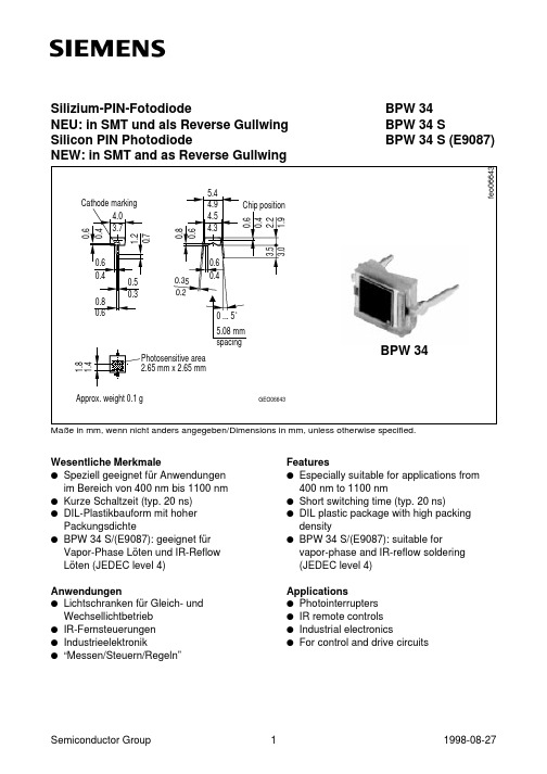
Photosensitive area 2.65 mm x 2.65 mm
BPW 34
1.4
1.8
Approx. weight 0.1 g
GEO06643
Maße in mm, wenn nicht anders angegeben/Dimensions in mm, unless otherwise specified.
10 3
Ι R nA
OHF00082
10 2
10 1
10 0
1000 TA
Directional characteristics Srel = f (ϕ)
40
30
20
10
0
ϕ 1.0
50 0.8
60
0.6
OHF01402
70
0.4
80
0.2
0 90
100
1.0
Wesentliche Merkmale q Speziell geeignet für Anwendungen
im Bereich von 400 nm bis 1100 nm q Kurze Schaltzeit (typ. 20 ns) q DIL-Plastikbauform mit hoher
0.8
0.6
0.4
0
20 40 60 80 100 120
Semiconductor Group
5
1998-08-27
Bezeichnung Description
Kurzschlußstrom, Ev = 1000 Ix
Short-circuit current
Anstiegs- und Abfallzeit des Fotostromes Rise and fall time of the photocurrent
cmy 210中文资料
fLO
L3
C3
L4
C4
MHz
nH
pF
nH
pF
500
15
82
47
82
750
6.8
33
22
33
800
6.8
33
18
33
950
6.8
27
15
27
Data Book
4
03.00
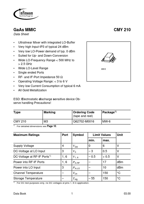
CMY 210
Typical Lumped Element Values for Different LO-Frequencies (cont’d)
> 2.5 GHz • Wide LO-Level Range • Single ended Ports • RF- and IF-Port Impedance 50 Ω • Operating Voltage Range: < 3 to 6 V • Very low Current Consumption of typical 6 mA • All Gold Metallization
CMY 210
MW-6
ESD: Electrostatic discharge sensitive device Observe handling Precautions!
Type
Marking
CMY 210
M3
1) For detailed dimensions see Page 10.
Ordering Code (tape and reel)
Input Filter: Throughpass for the signal to be mixed; reflection of the mixed signal and the harmonics of both.
- 1、下载文档前请自行甄别文档内容的完整性,平台不提供额外的编辑、内容补充、找答案等附加服务。
- 2、"仅部分预览"的文档,不可在线预览部分如存在完整性等问题,可反馈申请退款(可完整预览的文档不适用该条件!)。
- 3、如文档侵犯您的权益,请联系客服反馈,我们会尽快为您处理(人工客服工作时间:9:00-18:30)。
Silizium-PIN-Fotodiode mit sehr kurzer SchaltzeitSilicon PIN Photodiode with Very Short Switching Time Wesentliche Merkmaleq Speziell geeignet für Anwendungen im Be-reich von 400 nm bis 1100 nm (SFH 203P)und bei 880 nm (SFH 203PFA)q Kurze Schaltzeit (typ. 5 ns)q 5 mm-Plastikbauform im LED-Gehäuse Anwendungenq Industrieelektronikq “Messen/Steuern/Regeln”q Schnelle Lichtschranken für Gleich- und Wechsellichtbetrieb q LWLFeaturesq Especially suitable for applications from400 nm to 1100 nm (SFH 203P) and of 880 nm (SFH 203PFA)q Short switching time (typ. 5 ns)q 5 mm LED plastic package Applicationsq Industrial electronicsq For control and drive circuits q Photointerruptersq Fiber optic transmission systemsTyp (*vorher)Type (*formerly)Bestellnummer Ordering Code SFH 203 P (*SFH 217)Q62702-P946SFH 203 PFA (*SFH 217 F)Q62702-P947SFH 203 P SFH 203 PFAMaße in mm, wenn nicht anders angegeben/Dimensions in mm, unless otherwise specified.f e o 06644f e o f 6644GrenzwerteMaximum Ratings Bezeichnung DescriptionSymbol SymbolWert Value Einheit Unit Betriebs- und LagertemperaturOperating and storage temperature range T op ;T stg – 55...+ 100°C Löttemperatur (Lötstelle 2 mm vom Gehäuse entfernt bei Lötzeit t ≤ 3 s)Soldering temperature in 2 mm distance from case bottom (t ≤ 3 s)T S300°CSperrspannung Reverse voltage V R 50V VerlustleistungTotal power dissipationP tot100mWKennwerte (T A = 25°C)Characteristics Bezeichnung DescriptionSymbol SymbolWert ValueEinheit UnitSFH 203 PSFH 203 PFAFotoempfindlichkeit Spectral sensitivityV R = 5 V, Normlicht/standard light A,T = 2856 KV R = 5 V,λ = 950 nm,E e = 1 mW/cm 2S S9.5 (≥ 5)––6.2 (≥ 3.6)nA/Ix µA Wellenlänge der max. Fotoempfindlichkeit Wavelength of max. sensitivityλS max 850900nm Spektraler Bereich der Fotoempfindlichkeit S = 10 % von S maxSpectral range of sensitivity S = 10 % of S maxλ400...1100750 (1100)nmBestrahlungsempfindliche Fläche Radiant sensitive areaA 11mm 2Abmessung der bestrahlungsempfindlichen FlächeDimensions of radiant sensitive area L ×B L ×W 1×11×1mm ×mmAbstand Chipoberfläche zu Gehäuseober-flächeDistance chip front to case surfaceH0.4...0.70.4...0.7mmHalbwinkel Half angleϕ±75±75Grad deg.Dunkelstrom,V R = 20 V Dark currentI R 1 (≤ 10) 1 (≤ 10)nA Spektrale Fotoempfindlichkeit,λ = 850 nm Spectral sensitivityS λ0.620.59A/W Quantenausbeute,λ = 850 nm Quantum yieldη0.890.86Electrons Photon Leerlaufspannung Open-circuit voltageE v = 1000 Ix, Normlicht/standard light A,T = 2856 KE e = 0.5 mW/cm 2,λ = 950 nmV O V O350 (≥ 300)––300 (≥ 250)mV mVKurzschlußstrom Short-circuit currentE v = 1000 Ix, Normlicht/standard light A,T = 2856 KE e = 0.5 mW/cm 2,λ = 950 nmI SC I SC9.3––3.0µA µA Anstiegs- und Abfallzeit des Fotostromes Rise and fall time of the photocurrentR L = 50Ω;V R = 20 V;λ = 850 nm;I p = 800µA t r ,t f 55nsDurchlaßspannung,I F = 80 mA,E = 0Forward voltageV F 1.3 1.3V Kapazität,V R = 0 V,f = 1 MHz,E = 0CapacitanceC 01111pF Temperaturkoeffizient von V O Temperature coefficient of V O TC V – 2.6– 2.6mV/K Temperaturkoeffizient von I SC Temperature coefficient of I SC Normlicht/standard light A λ = 950 nmTC I0.18––0.2%/KRauschäquivalente Strahlungsleistung Noise equivalent power V R = 20 V,λ = 850 nmNEP2.9×10– 142.9×10– 14W √Hz Nachweisgrenze,V R = 20 V,λ = 850 nm Detection limitD*3.5×10¹² 3.5×1012cm ·√Hz WKennwerte (T A = 25°C)Characteristics (cont’d)Bezeichnung Description Symbol Symbol Wert ValueEinheit UnitSFH 203 PSFH 203 PFARelative spectral sensitivity SFH 203 P S rel =f (λ)Photocurrent I P =f (E e ),V R = 5 V Open-circuit voltage V O =f (E e )SFH 203 PFA Relative spectr. sensitivity SFH 203PFA S rel =f (λ)Photocurrent I P =f (E v ),V R = 5 V Open-circuit voltage V O =f (E v )SFH 203PTotal power dissipation P tot =f (T A )Dark current I R =f (V R ),E = 0CapacitanceC =f (V R ),f = 1 MHz,E= 0Directional characteristics S rel =f (ϕ)。