L7805
L7815CD2T中文资料

L7800SERIESPOSITIVE VOLTAGE REGULATORSJanuary 1997s OUTPUT CURRENT UP TO 1.5AsOUTPUT VOLTAGES OF 5;5.2;6;8;8.5;9;12;15;18;24Vs THERMAL OVERLOAD PROTECTION s SHORT CIRCUIT PROTECTIONsOUTPUT TRANSITION SOA PROTECTIONDESCRIPTIONThe L7800series of three-terminal positive regulators is available in TO-220ISOWATT220TO-3and D 2PAK packages and several fixed output voltages,making it useful in a wide range of applications.These regulators can provide local on-card regulation,eliminating the distribution problems associated with single point regulation.Each type employs internal current limiting,thermal shut-down and safe area protection,making it essentially indestructible.If adequate heat sinking is provided,they can deliver over 1A output current.Although designed primarily as fixed voltage regulators,these devices can be used with external components to obtain adjustable voltages and currents.12TO-3123TO-220ISOWATT22012313D 2PAKBLOCK DIAGRAM1/25CONNECTION DIAGRAM AND ORDERING NUMBERS (top view)TO-220&ISOWATT220TO-3D 2PAKTHERMAL DATASymbolParameterD 2PAK TO-220ISOWATT220TO-3UnitR t hj-case R th j-a mb Thermal Resistance Junction-case Max Thermal Resistance Junction-ambient Max 362.5350460435o C/W oC/WType TO-220D 2PAK (*)ISOWATT220TO-3Output VoltageL7805L7805C L7852C L7806L7806C L7808L7808C L7885C L7809C L7812L7812C L7815L7815C L7818L7818C L7820L7820C L7824L7824CL7805CV L7852CV L7806CV L7808CV L7885CV L7809CV L7812CV L7815CV L7818CV L7820CV L7824CVL7805CD2T L7852CD2T L7806CD2T L7808CD2T L7885CD2T L7809CD2T L7812CD2T L7815CD2T L7818CD2T L7820CD2T L7824CD2TL7805CP L7852CP L7806CP L7808CP L7885CP L7809CP L7812CP L7815CP L7818CP L7820CP L7824CPL7805T L7805CT L7852CT L7806T L7806CT L7808T L7808CT L7885CT L7809CT L7812T L7812CT L7815T L7815CT L7818T L7818CT L7820T L7820CT L7824T L7824CT5V 5V 5.2V 6V 6V 8V 8V 8.5V 9V 12V 12V 15V 15V 18V 18V 20V 20V 24V 24V(*)AVAILABLE IN TAPE AND REEL WITH ”-TR”SUFFIXABSOLUTE MAXIMUM RATINGSSymbol ParameterValue Unit V i DC Input Voltage (for V O =5to 18V)(for V O =20,24V)3540V VI o Output Current Internally limited P t ot Power DissipationInternally limited T o p Operating Junction Temperature Range (for L7800)(for L7800C )-55to 1250to 150o C o C T stgStorage Temperature Range-40to 150oCL78002/25L7800 APPLICATION CIRCUITSCHEMATIC DIAGRAM3/25TEST CIRCUITSFigure3:Ripple Rejection.Figure2:Load Regulation.Figure1:DC Parameter L78004/25ELECTRICAL CHARACTERISTICS FOR L7806(refer to the test circuits,T j =-55to 150o C,V i =15V,I o =500mA,C i =0.33µF,C o =0.1µF unless otherwise specified)Symbol ParameterTest Conditions Min.Typ.Max.Unit V o Output Voltage T j =25oC 5.756 6.25V V o Output Voltage I o =5mA to 1A P o ≤15WV i =9to 21V 5.6566.35V ∆V o *Line Regulation V i =8to 25V T j =25oCV i =9to 13VT j =25oC6030mV mV ∆V o *Load Regulation I o =5to 1500mA T j =25o CI o =250to 750mA T j =25oC10030mV mV I d Quiescent Current T j =25o C 6mA ∆I d Quiescent Current Change I o =5to 1000mA 0.5mA ∆I d Quiescent Current Change V i =9to 25V 0.8mA ∆V o ∆T Output Voltage Drift I o =5mA0.7mV/oCeN Output Noise Voltage B =10Hz to 100KHz T j =25oC 40µV/V O SVR Supply Voltage Rejection V i =9to 19V f =120Hz65dB V d Dropout Voltage I o =1A T j =25o C2 2.5V R o Output Resistance f =1KHz 19m ΩI sc Short Circuit Current V i =35V T j =25oC0.75 1.2A I s cpShort Circuit Peak CurrentT j =25o C1.32.23.3AELECTRICAL CHARACTERISTICS FOR L7805(refer to the test circuits,T j =-55to 150o C,V i =10V,I o =500mA,C i =0.33µF,C o =0.1µF unless otherwise specified)Symbol ParameterTest Conditions Min.Typ.Max.Unit V o Output Voltage T j =25oC 4.85 5.2V V o Output Voltage I o =5mA to 1A P o ≤15WV i =8to 20V 4.655 5.35V ∆V o *Line Regulation V i =7to 25V T j =25o CV i =8to 12VT j =25oC315025mV mV ∆V o *Load Regulation I o =5to 1500mA T j =25oCI o =250to 750mA T j =25oC10025mV mV I d Quiescent Current T j =25o C 6mA ∆I d Quiescent Current Change I o =5to 1000mA 0.5mA ∆I d Quiescent Current Change V i =8to 25V 0.8mA ∆V o ∆T Output Voltage Drift I o =5mA0.6mV/oCeN Output Noise Voltage B =10Hz to 100KHz T j =25o C 40µV/V O SVR Supply Voltage Rejection V i =8to 18V f =120Hz68dB V d Dropout Voltage I o =1A T j =25oC 2 2.5V R o Output Resistance f =1KHz 17m ΩI sc Short Circuit Current V i =35V T j =25oC0.75 1.2A I s cpShort Circuit Peak CurrentT j =25oC1.32.23.3A*Load and line regulation are specified at constant junction temperature.Changes in V o due to heating effects must be taken into account separately.Pulce testing with low duty cycle is used.L78005/25ELECTRICAL CHARACTERISTICS FOR L7812(refer to the test circuits,T j =-55to 150o C,V i =19V,I o =500mA,C i =0.33µF,C o =0.1µF unless otherwise specified)Symbol ParameterTest Conditions Min.Typ.Max.Unit V o Output Voltage T j =25oC11.51212.5V V o Output Voltage I o =5mA to 1A P o ≤15W V i =15.5to 27V11.41212.6V ∆V o *Line Regulation V i =14.5to 30V T j =25oCV i =16to 22V T j =25oC 12060mV mV ∆V o *Load Regulation I o =5to 1500mA T j =25o CI o =250to 750mA T j =25oC10060mV mV I d Quiescent Current T j =25o C 6mA ∆I d Quiescent Current Change I o =5to 1000mA 0.5mA ∆I d Quiescent Current Change V i =15to 30V 0.8mA ∆V o ∆T Output Voltage Drift I o =5mA1.5mV/oCeN Output Noise Voltage B =10Hz to 100KHz T j =25o C 40µV/V O SVR Supply Voltage Rejection V i =15to 25V f =120Hz61dB V d Dropout Voltage I o =1A T j =25o C2 2.5V R o Output Resistance f =1KHz 18m ΩI sc Short Circuit Current V i =35V T j =25oC0.75 1.2A I s cpShort Circuit Peak CurrentT j =25o C1.32.23.3AELECTRICAL CHARACTERISTICS FOR L7808(refer to the test circuits,T j =-55to 150o C,V i =14V,I o =500mA,C i =0.33µF,C o =0.1µF unless otherwise specified)Symbol ParameterTest Conditions Min.Typ.Max.Unit V o Output Voltage T j =25oC7.788.3V V o Output Voltage I o =5mA to 1A P o ≤15W V i =11.5to 23V7.688.4V ∆V o *Line Regulation V i =10.5to 25V T j =25o CV i =11to 17V T j =25oC 8040mV mV ∆V o *Load Regulation I o =5to 1500mA T j =25oCI o =250to 750mA T j =25oC10040mV mV I d Quiescent Current T j =25o C 6mA ∆I d Quiescent Current Change I o =5to 1000mA 0.5mA ∆I d Quiescent Current Change V i =11.5to 25V 0.8mA ∆V o ∆T Output Voltage Drift I o =5mA1mV/oCeN Output Noise Voltage B =10Hz to 100KHz T j =25o C 40µV/V O SVR Supply Voltage Rejection V i =11.5to 21.5V f =120Hz62dB V d Dropout Voltage I o =1A T j =25oC 2 2.5V R o Output Resistance f =1KHz 16m ΩI sc Short Circuit Current V i =35V T j =25oC0.75 1.2A I s cpShort Circuit Peak CurrentT j =25oC1.32.23.3A*Load and line regulation are specified at constant junction temperature.Changes in V o due to heating effects must be taken into account separately.Pulce testing with low duty cycle is used.L78006/25ELECTRICAL CHARACTERISTICS FOR L7818(refer to the test circuits,T j =-55to 150o C,V i =26V,I o =500mA,C i =0.33µF,C o =0.1µF unless otherwise specified)Symbol ParameterTest Conditions Min.Typ.Max.Unit V o Output Voltage T j =25oC 17.31818.7V V o Output Voltage I o =5mA to 1A P o ≤15W V i =22to 33V 17.11818.9V ∆V o *Line Regulation V i =21to 33V T j =25oCV i =24to 30VT j =25oC18090mV mV ∆V o *Load Regulation I o =5to 1500mA T j =25o CI o =250to 750mA T j =25oC18090mV mV I d Quiescent Current T j =25o C 6mA ∆I d Quiescent Current Change I o =5to 1000mA 0.5mA ∆I d Quiescent Current Change V i =22to 33V 0.8mA ∆V o ∆T Output Voltage Drift I o =5mA2.3mV/oCeN Output Noise Voltage B =10Hz to 100KHz T j =25oC 40µV/V O SVR Supply Voltage Rejection V i =22to 32V f =120Hz59dB V d Dropout Voltage I o =1A T j =25o C2 2.5V R o Output Resistance f =1KHz 22m ΩI sc Short Circuit Current V i =35V T j =25oC0.75 1.2A I s cpShort Circuit Peak CurrentT j =25o C1.32.23.3AELECTRICAL CHARACTERISTICS FOR L7815(refer to the test circuits,T j =-55to 150o C,V i =23V,I o =500mA,C i =0.33µF,C o =0.1µF unless otherwise specified)Symbol ParameterTest Conditions Min.Typ.Max.Unit V o Output Voltage T j =25oC14.41515.6V V o Output Voltage I o =5mA to 1A P o ≤15W V i =18.5to 30V14.251515.75V ∆V o *Line Regulation V i =17.5to 30V T j =25o CV i =20to 26V T j =25oC 15075mV mV ∆V o *Load Regulation I o =5to 1500mA T j =25oCI o =250to 750mA T j =25oC15075mV mV I d Quiescent Current T j =25o C 6mA ∆I d Quiescent Current Change I o =5to 1000mA 0.5mA ∆I d Quiescent Current Change V i =18.5to 30V 0.8mA ∆V o ∆T Output Voltage Drift I o =5mA1.8mV/oCeN Output Noise Voltage B =10Hz to 100KHz T j =25o C 40µV/V O SVR Supply Voltage Rejection V i =18.5to 28.5V f =120Hz60dB V d Dropout Voltage I o =1A T j =25oC 2 2.5V R o Output Resistance f =1KHz 19m ΩI sc Short Circuit Current V i =35V T j =25oC0.75 1.2A I s cpShort Circuit Peak CurrentT j =25oC1.32.23.3A*Load and line regulation are specified at constant junction temperature.Changes in V o due to heating effects must be taken into account separately.Pulce testing with low duty cycle is used.L78007/25ELECTRICAL CHARACTERISTICS FOR L7824(refer to the test circuits,T j =-55to 150o C,V i =33V,I o =500mA,C i =0.33µF,C o =0.1µF unless otherwise specified)Symbol ParameterTest Conditions Min.Typ.Max.Unit V o Output Voltage T j =25oC 232425V V o Output Voltage I o =5mA to 1A P o ≤15W V i =28to 38V 22.82425.2V ∆V o *Line Regulation V i =27to 38V T j =25oCV i =30to 36VT j =25oC240120mV mV ∆V o *Load Regulation I o =5to 1500mA T j =25o CI o =250to 750mA T j =25oC240120mV mV I d Quiescent Current T j =25o C 6mA ∆I d Quiescent Current Change I o =5to 1000mA 0.5mA ∆I d Quiescent Current Change V i =28to 38V 0.8mA ∆V o ∆T Output Voltage Drift I o =5mA3mV/oCeN Output Noise Voltage B =10Hz to 100KHz T j =25oC 40µV/V O SVR Supply Voltage Rejection V i =28to 38V f =120Hz56dB V d Dropout Voltage I o =1A T j =25o C2 2.5V R o Output Resistance f =1KHz 28m ΩI sc Short Circuit Current V i =35V T j =25oC0.75 1.2A I s cpShort Circuit Peak CurrentT j =25o C1.32.23.3AELECTRICAL CHARACTERISTICS FOR L7820(refer to the test circuits,T j =-55to 150o C,V i =28V,I o =500mA,C i =0.33µF,C o =0.1µF unless otherwise specified)Symbol ParameterTest Conditions Min.Typ.Max.Unit V o Output Voltage T j =25oC 19.22020.8V V o Output Voltage I o =5mA to 1A P o ≤15WV i =24to 35V192021V ∆V o *Line Regulation V i =22.5to 35V T j =25o CV i =26to 32V T j =25oC 200100mV mV ∆V o *Load Regulation I o =5to 1500mA T j =25oCI o =250to 750mA T j =25oC200100mV mV I d Quiescent Current T j =25o C 6mA ∆I d Quiescent Current Change I o =5to 1000mA 0.5mA ∆I d Quiescent Current Change V i =24to 35V 0.8mA ∆V o ∆T Output Voltage Drift I o =5mA2.5mV/oCeN Output Noise Voltage B =10Hz to 100KHz T j =25o C 40µV/V O SVR Supply Voltage Rejection V i =24to 35V f =120Hz58dB V d Dropout Voltage I o =1A T j =25oC 2 2.5V R o Output Resistance f =1KHz 24m ΩI sc Short Circuit Current V i =35V T j =25oC0.75 1.2A I s cpShort Circuit Peak CurrentT j =25oC1.32.23.3A*Load and line regulation are specified at constant junction temperature.Changes in V o due to heating effects must be taken into account separately.Pulce testing with low duty cycle is used.L78008/25ELECTRICAL CHARACTERISTICS FOR L7852C (refer to the test circuits,T j =0to 125o C,V i =10V,I o =500mA,C i =0.33µF,C o =0.1µF unless otherwise specified)Symbol ParameterTest Conditions Min.Typ.Max.Unit V o Output Voltage T j =25oC 5.0 5.2 5.4V V o Output Voltage I o =5mA to 1A P o ≤15WV i =8to 20V 4.955.2 5.45V ∆V o *Line Regulation V i =7to 25V T j =25oCV i =8to 12VT j =25oC3110552mV mV ∆V o *Load Regulation I o =5to 1500mA T j =25o CI o =250to 750mA T j =25oC10552mV mV I d Quiescent Current T j =25o C 8mA ∆I d Quiescent Current Change I o =5to 1000mA 0.5mA ∆I d Quiescent Current Change V i =7to 25V 1.3mA ∆V o ∆T Output Voltage Drift I o =5mA-1.0mV/oC eN Output Noise Voltage B =10Hz to 100KHz T j =25oC 42µV SVR Supply Voltage Rejection V i =8to 18V f =120Hz61dB V d Dropout Voltage I o =1A T j =25o C2V R o Output Resistance f =1KHz 17m ΩI sc Short Circuit Current V i =35V T j =25oC750mA I s cpShort Circuit Peak CurrentT j =25o C2.2AELECTRICAL CHARACTERISTICS FOR L7805C (refer to the test circuits,T j =0to 125o C,V i =10V,I o =500mA,C i =0.33µF,C o =0.1µF unless otherwise specified)Symbol ParameterTest Conditions Min.Typ.Max.Unit V o Output Voltage T j =25oC 4.85 5.2V V o Output Voltage I o =5mA to 1A P o ≤15WV i =7to 20V 4.755 5.25V ∆V o *Line Regulation V i =7to 25V T j =25o CV i =8to 12VT j =25oC3110050mV mV ∆V o *Load Regulation I o =5to 1500mA T j =25oCI o =250to 750mA T j =25oC10050mV mV I d Quiescent Current T j =25o C 8mA ∆I d Quiescent Current Change I o =5to 1000mA 0.5mA ∆I d Quiescent Current Change V i =7to 25V 0.8mA ∆V o ∆T Output Voltage Drift I o =5mA-1.1mV/oC eN Output Noise Voltage B =10Hz to 100KHz T j =25o C 40µV SVR Supply Voltage Rejection V i =8to 18V f =120Hz62dB V d Dropout Voltage I o =1A T j =25oC2V R o Output Resistance f =1KHz 17m ΩI sc Short Circuit Current V i =35V T j =25oC750mA I s cpShort Circuit Peak CurrentT j =25oC2.2A*Load and line regulation are specified at constant junction temperature.Changes in V o due to heating effects must be taken into account separately.Pulce testing with low duty cycle is used.L78009/25ELECTRICAL CHARACTERISTICS FOR L7808C (refer to the test circuits,T j =0to 125o C,V i =14V,I o =500mA,C i =0.33µF,C o =0.1µF unless otherwise specified)Symbol ParameterTest Conditions Min.Typ.Max.Unit V o Output Voltage T j =25oC7.788.3V V o Output Voltage I o =5mA to 1A P o ≤15W V i =10.5to 25V7.688.4V ∆V o *Line Regulation V i =10.5to 25V T j =25oCV i =11to 17V T j =25oC 16080mV mV ∆V o *Load Regulation I o =5to 1500mA T j =25o CI o =250to 750mA T j =25oC16080mV mV I d Quiescent Current T j =25o C 8mA ∆I d Quiescent Current Change I o =5to 1000mA 0.5mA ∆I d Quiescent Current Change V i =10.5to 25V 1mA ∆V o ∆T Output Voltage Drift I o =5mA-0.8mV/oC eN Output Noise Voltage B =10Hz to 100KHz T j =25o C 52µV SVR Supply Voltage Rejection V i =11.5to 21.5V f =120Hz56dB V d Dropout Voltage I o =1A T j =25o C2V R o Output Resistance f =1KHz 16m ΩI sc Short Circuit Current V i =35V T j =25oC450mA I s cpShort Circuit Peak CurrentT j =25o C2.2AELECTRICAL CHARACTERISTICS FOR L7806C (refer to the test circuits,T j =0to 125o C,V i =11V,I o =500mA,C i =0.33µF,C o =0.1µF unless otherwise specified)Symbol ParameterTest Conditions Min.Typ.Max.Unit V o Output Voltage T j =25oC 5.756 6.25V V o Output Voltage I o =5mA to 1A P o ≤15WV i =8to 21V 5.766.3V ∆V o *Line Regulation V i =8to 25V T j =25o CV i =9to 13VT j =25oC12060mV mV ∆V o *Load Regulation I o =5to 1500mA T j =25oCI o =250to 750mA T j =25oC12060mV mV I d Quiescent Current T j =25o C 8mA ∆I d Quiescent Current Change I o =5to 1000mA 0.5mA ∆I d Quiescent Current Change V i =8to 25V 1.3mA ∆V o ∆T Output Voltage Drift I o =5mA-0.8mV/oC eN Output Noise Voltage B =10Hz to 100KHz T j =25o C 45µV SVR Supply Voltage Rejection V i =9to 19V f =120Hz59dB V d Dropout Voltage I o =1A T j =25oC 2V R o Output Resistance f =1KHz 19m ΩI sc Short Circuit Current V i =35V T j =25oC550mA I s cpShort Circuit Peak CurrentT j =25oC2.2A*Load and line regulation are specified at constant junction temperature.Changes in V o due to heating effects must be taken into account separately.Pulce testing with low duty cycle is used.L780010/25ELECTRICAL CHARACTERISTICS FOR L7809C (refer to the test circuits,T j =0to 125o C,V i =15V,I o =500mA,C i =0.33µF,C o =0.1µF unless otherwise specified)Symbol ParameterTest Conditions Min.Typ.Max.Unit V o Output Voltage T j =25oC8.6599.35V V o Output Voltage I o =5mA to 1A P o ≤15W V i =11.5to 26V8.5599.45V ∆V o *Line Regulation V i =11.5to 26V T j =25oCV i =12to 18V T j =25oC 18090mV mV ∆V o *Load Regulation I o =5to 1500mA T j =25o CI o =250to 750mA T j =25oC18090mV mV I d Quiescent Current T j =25o C 8mA ∆I d Quiescent Current Change I o =5to 1000mA 0.5mA ∆I d Quiescent Current Change V i =11.5to 26V 1mA ∆V o ∆T Output Voltage Drift I o =5mA-1.0mV/oC eN Output Noise Voltage B =10Hz to 100KHz T j =25o C 70µV SVR Supply Voltage Rejection V i =12to 23V f =120Hz55dB V d Dropout Voltage I o =1A T j =25o C2V R o Output Resistance f =1KHz 17m ΩI sc Short Circuit Current V i =35V T j =25oC400mA I s cpShort Circuit Peak CurrentT j =25o C2.2AELECTRICAL CHARACTERISTICS FOR L7885C (refer to the test circuits,T j =0to 125o C,V i =14.5V,I o =500mA,C i =0.33µF,C o =0.1µF unless otherwise specified)Symbol ParameterTest Conditions Min.Typ.Max.Unit V o Output Voltage T j =25oC 8.28.58.8V V o Output Voltage I o =5mA to 1A P o ≤15WV i =11to 26V8.18.58.9V ∆V o *Line Regulation V i =11to 27V T j =25o CV i =11.5to 17.5V T j =25oC 16080mV mV ∆V o *Load Regulation I o =5to 1500mA T j =25oCI o =250to 750mA T j =25oC16080mV mV I d Quiescent Current T j =25o C 8mA ∆I d Quiescent Current Change I o =5to 1000mA 0.5mA ∆I d Quiescent Current Change V i =11to 27V 1mA ∆V o ∆T Output Voltage Drift I o =5mA-0.8mV/oC eN Output Noise Voltage B =10Hz to 100KHz T j =25o C 55µV SVR Supply Voltage Rejection V i =12to 22V f =120Hz56dB V d Dropout Voltage I o =1A T j =25oC2V R o Output Resistance f =1KHz 16m ΩI sc Short Circuit Current V i =35V T j =25oC450mA I s cpShort Circuit Peak CurrentT j =25oC2.2A*Load and line regulation are specified at constant junction temperature.Changes in V o due to heating effects must be taken into account separately.Pulce testing with low duty cycle is used.11/25ELECTRICAL CHARACTERISTICS FOR L7815C (refer to the test circuits,T j =0to 125o C,V i =23V,I o =500mA,C i =0.33µF,C o =0.1µF unless otherwise specified)Symbol ParameterTest Conditions Min.Typ.Max.Unit V o Output Voltage T j =25oC14.41515.6V V o Output Voltage I o =5mA to 1A P o ≤15W V i =17.5to 30V14.251515.75V ∆V o *Line Regulation V i =17.5to 30V T j =25oCV i =20to 26V T j =25oC 300150mV mV ∆V o *Load Regulation I o =5to 1500mA T j =25o CI o =250to 750mA T j =25oC300150mV mV I d Quiescent Current T j =25o C 8mA ∆I d Quiescent Current Change I o =5to 1000mA 0.5mA ∆I d Quiescent Current Change V i =17.5to 30V 1mA ∆V o ∆T Output Voltage Drift I o =5mA-1mV/oC eN Output Noise Voltage B =10Hz to 100KHz T j =25o C 90µV SVR Supply Voltage Rejection V i =18.5to 28.5V f =120Hz54dB V d Dropout Voltage I o =1A T j =25o C2V R o Output Resistance f =1KHz 19m ΩI sc Short Circuit Current V i =35V T j =25oC230mA I s cpShort Circuit Peak CurrentT j =25o C2.1AELECTRICAL CHARACTERISTICS FOR L7812C (refer to the test circuits,T j =0to 125o C,V i =19V,I o =500mA,C i =0.33µF,C o =0.1µF unless otherwise specified)Symbol ParameterTest Conditions Min.Typ.Max.Unit V o Output Voltage T j =25oC11.51212.5V V o Output Voltage I o =5mA to 1A P o ≤15W V i =14.5to 27V11.41212.6V ∆V o *Line Regulation V i =14.5to 30V T j =25o CV i =16to 22V T j =25oC 240120mV mV ∆V o *Load Regulation I o =5to 1500mA T j =25oCI o =250to 750mA T j =25oC240120mV mV I d Quiescent Current T j =25o C 8mA ∆I d Quiescent Current Change I o =5to 1000mA 0.5mA ∆I d Quiescent Current Change V i =14.5to 30V 1mA ∆V o ∆T Output Voltage Drift I o =5mA-1mV/oC eN Output Noise Voltage B =10Hz to 100KHz T j =25o C 75µV SVR Supply Voltage Rejection V i =15to 25V f =120Hz55dB V d Dropout Voltage I o =1A T j =25oC2V R o Output Resistance f =1KHz 18m ΩI sc Short Circuit Current V i =35V T j =25oC350mA I s cpShort Circuit Peak CurrentT j =25o C2.2A*Load and line regulation are specified at constant junction temperature.Changes in V o due to heating effects must be taken into account separately.Pulce testing with low duty cycle is used.12/25ELECTRICAL CHARACTERISTICS FOR L7820C (refer to the test circuits,T j =0to 125o C,V i =28V,I o =500mA,C i =0.33µF,C o =0.1µF unless otherwise specified)Symbol ParameterTest Conditions Min.Typ.Max.Unit V o Output Voltage T j =25oC 19.22020.8V V o Output Voltage I o =5mA to 1A P o ≤15WV i =23to 35V192021V ∆V o *Line Regulation V i =22.5to 35V T j =25oCV i =26to 32V T j =25oC 400200mV mV ∆V o *Load Regulation I o =5to 1500mA T j =25o CI o =250to 750mA T j =25oC400200mV mV I d Quiescent Current T j =25o C 8mA ∆I d Quiescent Current Change I o =5to 1000mA 0.5mA ∆I d Quiescent Current Change V i =23to 35V 1mA ∆V o ∆T Output Voltage Drift I o =5mA-1mV/oC eN Output Noise Voltage B =10Hz to 100KHz T j =25oC 150µV SVR Supply Voltage Rejection V i =24to 35V f =120Hz52dB V d Dropout Voltage I o =1A T j =25o C2V R o Output Resistance f =1KHz 24m ΩI sc Short Circuit Current V i =35V T j =25oC180mA I s cpShort Circuit Peak CurrentT j =25o C2.1AELECTRICAL CHARACTERISTICS FOR L7818C (refer to the test circuits,T j =0to 125o C,V i =26V,I o =500mA,C i =0.33µF,C o =0.1µF unless otherwise specified)Symbol ParameterTest Conditions Min.Typ.Max.Unit V o Output Voltage T j =25oC 17.31818.7V V o Output Voltage I o =5mA to 1A P o ≤15W V i =21to 33V 17.11818.9V ∆V o *Line Regulation V i =21to 33V T j =25o CV i =24to 30VT j =25oC360180mV mV ∆V o *Load Regulation I o =5to 1500mA T j =25oCI o =250to 750mA T j =25oC360180mV mV I d Quiescent Current T j =25o C 8mA ∆I d Quiescent Current Change I o =5to 1000mA 0.5mA ∆I d Quiescent Current Change V i =21to 33V 1mA ∆V o ∆T Output Voltage Drift I o =5mA-1mV/oC eN Output Noise Voltage B =10Hz to 100KHz T j =25o C 110µV SVR Supply Voltage Rejection V i =22to 32V f =120Hz53dB V d Dropout Voltage I o =1A T j =25oC2V R o Output Resistance f =1KHz 22m ΩI sc Short Circuit Current V i =35V T j =25oC200mA I s cpShort Circuit Peak CurrentT j =25oC2.1A*Load and line regulation are specified at constant junction temperature.Changes in V o due to heating effects must be taken into account separately.Pulce testing with low duty cycle is used.13/25*Load and line regulation are specified at constant junction temperature.Changes in V o due to heating effects must be taken into account separately.Pulce testing with low duty cycle is used.ELECTRICAL CHARACTERISTICS FOR L7824C (refer to the test circuits,T j =0to 125o C,V i =33V,I o =500mA,C i =0.33µF,C o =0.1µF unless otherwise specified)Symbol ParameterTest Conditions Min.Typ.Max.Unit V o Output Voltage T j =25oC 232425V V o Output Voltage I o =5mA to 1A P o ≤15W V i =27to 38V 22.82425.2V ∆V o *Line Regulation V i =27to 38V T j =25o CV i =30to 36VT j =25oC480240mV mV ∆V o *Load Regulation I o =5to 1500mA T j =25oCI o =250to 750mA T j =25oC480240mV mV I d Quiescent Current T j =25o C 8mA ∆I d Quiescent Current Change I o =5to 1000mA 0.5mA ∆I d Quiescent Current Change V i =27to 38V 1mA ∆V o ∆T Output Voltage Drift I o =5mA-1.5mV/oC eN Output Noise Voltage B =10Hz to 100KHz T j =25o C 170µV SVR Supply Voltage Rejection V i =28to 38V f =120Hz50dB V d Dropout Voltage I o =1A T j =25oC2V R o Output Resistance f =1KHz 28m ΩI sc Short Circuit Current V i =35V T j =25oC150mA I s cpShort Circuit Peak CurrentT j =25oC2.1A14/25Figure 8:Output Impedance vs.Frequency.Figure 9:Quiescent Current vs.JunctionTemperature.Figure 4:Dropout Voltage vs.JunctionTemperature.Figure 5:Peak Output Current vs.Input/outputDifferential Voltage.Figure 6:Supply Voltage Rejection vs.Frequency.Figure 7:Output Voltage vs.JunctionTemperature.15/25Figure12:Quiescent Current vs.InputVoltage.Figure13:Fixed Output Regulator.Figure14:Current Regulator. Figure10:Load Transient Response.Figure11:Line Transient Response.NOTE:1.To specify an output voltage,substitute voltage value for”XX”.2.Although no output capacitor is need for stability,it does improve transient response.3.Required if cregulator is locate an appreciable distance from power supply filter.I O=V XXR1+I d16/25Figure 15:Circuit for Increasing OutputVoltage.Figure 16:Adjustable Output Regulator(7to 30V).Figure 17:0.5to 10V Regulator.Figure 18:High Current Voltage Regulator.I R1≥5I d V O =V XX (1+R 2R 1)+I d R 2VO =V XXR 4R 1R 1=V BEQ 1I REQ −I Q 1βQ 1I O =I REG +Q 1(I REG −V BEQ 1R 1)17/25Figure 19:High Output Current with ShortCircuit Protection.Figure 20:Tracking Voltage Regulator.Figure 21:Split Power Supply (±15V –1A).Figure 22:Negative Output Voltage Circuit.Figure 23:Switching Regulator.Figure 24:High Input Voltage Circuit.V IN =V i -(V Z +V BE )*Against potential latch-up problems.R SC =V BEQ 2I SC18/25Figure 27:High Input and Output Voltage.Figure 28:Reducing Power Dissipation withDr opping Resistor.Figure 29:Remote Shutdown.Figure 25:High Input Voltage Circuit.Figure 26:High Output Voltage Regulator.V O =V XX +V Z1R =V i (min )−V XX −V DROP (max )I O (max )+I d (max )19/25Figure 30:Power AM Modulator (unity voltagegain,I o <1A).Figure 31:Adjustable Output Voltage withTemperatureCompensation.NOTE:The circuit performs well up to 100KHzNOTE:Q 2is connected as a diode in order to compensate the variation of the Q 1V BE with the temperature.C allows a slow rise-time of the V oFigure 32:Light Controllers (V o min =V xx +V BE ).Figure 33:Protection against Input Short-circuitwith High Capacitance Loads.Application with high capacitance loads and an output voltage greater than 6volts need an external diode (see fig.33)to protect the deviceagainst input short circuit.In this case the input voltage falls rapidly while the output voltage decrease slowly.The capacitance dischrges by means of the Base-Emitter junction of the series pass transistor in the regulator.If the energy is sufficently high,the transistor may be destroyed.The external diode by-passes the current from the IC to ground.V O falls when the light goes upV O rises when the light goes upV O =VXX(1+R 2R 1)+V BE 20/25。
L7805CV参数

March 2010Doc ID 2143 Rev 211/58L78xx - L78xxC L78xxAB - L78xxACPositive voltage regulatorsFeatures■Output current up to 1.5 A■Output voltages of 5; 6; 8; 8.5; 9; 12; 15; 18; 24 V■Thermal overload protection ■Short circuit protection■Output transition SOA protection ■ 2 % output voltage tolerance (A version)■Guaranteed in extended temperature range (A version)DescriptionThe L78xx series of three-terminal positiveregulators is available in TO-220, TO-220FP , TO-3, D²PAK and DPAK packages and several fixed output voltages, making it useful in a wide range of applications. These regulators can provide local on-card regulation, eliminating thedistribution problems associated with single point regulation. Each type employs internal current limiting, thermal shut-down and safe areaprotection, making it essentially indestructible. If adequate heat sinking is provided, they candeliver over 1 A output current. Although designed primarily as fixed voltage regulators, thesedevices can be used with external components to obtain adjustable voltage and currents.Table 1.Device summaryPart numbersL7805L7806AC L7809AB L7815AB L7805C L7808C L7809AC L7815AC L7805AB L7808AB L7812C L7818C L7805AC L7808AC L7812AB L7824C L7806C L7885C L7812AC L7824AB L7806ABL7809CL7815CL7824ACContents L78xx, L78xxC, L78xxAB, L78xxACContents1Diagram . . . . . . . . . . . . . . . . . . . . . . . . . . . . . . . . . . . . . . . . . . . . . . . . . . . 6 2Pin configuration . . . . . . . . . . . . . . . . . . . . . . . . . . . . . . . . . . . . . . . . . . . 7 3Maximum ratings . . . . . . . . . . . . . . . . . . . . . . . . . . . . . . . . . . . . . . . . . . . . 8 4Test circuits . . . . . . . . . . . . . . . . . . . . . . . . . . . . . . . . . . . . . . . . . . . . . . . . 9 5Electrical characteristics . . . . . . . . . . . . . . . . . . . . . . . . . . . . . . . . . . . . 106Application information . . . . . . . . . . . . . . . . . . . . . . . . . . . . . . . . . . . . . 296.1Design consideration . . . . . . . . . . . . . . . . . . . . . . . . . . . . . . . . . . . . . . . . 29 7Typical performance . . . . . . . . . . . . . . . . . . . . . . . . . . . . . . . . . . . . . . . . 39 8Package mechanical data . . . . . . . . . . . . . . . . . . . . . . . . . . . . . . . . . . . . 41 9Order codes . . . . . . . . . . . . . . . . . . . . . . . . . . . . . . . . . . . . . . . . . . . . . . 56 10Revision history . . . . . . . . . . . . . . . . . . . . . . . . . . . . . . . . . . . . . . . . . . . 572/58Doc ID 2143 Rev 21L78xx, L78xxC, L78xxAB, L78xxAC List of tables List of tablesTable 1.Device summary. . . . . . . . . . . . . . . . . . . . . . . . . . . . . . . . . . . . . . . . . . . . . . . . . . . . . . . . . . 1 Table 2.Absolute maximum ratings. . . . . . . . . . . . . . . . . . . . . . . . . . . . . . . . . . . . . . . . . . . . . . . . . . 8 Table 3.Thermal data. . . . . . . . . . . . . . . . . . . . . . . . . . . . . . . . . . . . . . . . . . . . . . . . . . . . . . . . . . . . . 8 Table 4.Electrical characteristics of L7805 . . . . . . . . . . . . . . . . . . . . . . . . . . . . . . . . . . . . . . . . . . . 10 Table 5.Electrical characteristics of L7805A . . . . . . . . . . . . . . . . . . . . . . . . . . . . . . . . . . . . . . . . . . 11 Table 6.Electrical characteristics of L7806A . . . . . . . . . . . . . . . . . . . . . . . . . . . . . . . . . . . . . . . . . . 12 Table 7.Electrical characteristics of L7808A . . . . . . . . . . . . . . . . . . . . . . . . . . . . . . . . . . . . . . . . . . 13 Table 8.Electrical characteristics of L7809A . . . . . . . . . . . . . . . . . . . . . . . . . . . . . . . . . . . . . . . . . . 14 Table 9.Electrical characteristics of L7812A . . . . . . . . . . . . . . . . . . . . . . . . . . . . . . . . . . . . . . . . . . 15 Table 10.Electrical characteristics of L7815A . . . . . . . . . . . . . . . . . . . . . . . . . . . . . . . . . . . . . . . . . . 16 Table 11.Electrical characteristics of L7824A . . . . . . . . . . . . . . . . . . . . . . . . . . . . . . . . . . . . . . . . . . 17 Table 12.Electrical characteristics of L7805C . . . . . . . . . . . . . . . . . . . . . . . . . . . . . . . . . . . . . . . . . . 18 Table 13.Electrical characteristics of L7806C . . . . . . . . . . . . . . . . . . . . . . . . . . . . . . . . . . . . . . . . . . 19 Table 14.Electrical characteristics of L7808C . . . . . . . . . . . . . . . . . . . . . . . . . . . . . . . . . . . . . . . . . . 20 Table 15.Electrical characteristics of L7885C . . . . . . . . . . . . . . . . . . . . . . . . . . . . . . . . . . . . . . . . . . 21 Table 16.Electrical characteristics of L7809C . . . . . . . . . . . . . . . . . . . . . . . . . . . . . . . . . . . . . . . . . . 22 Table 17.Electrical characteristics of L7810C . . . . . . . . . . . . . . . . . . . . . . . . . . . . . . . . . . . . . . . . . . 23 Table 18.Electrical characteristics of L7812C . . . . . . . . . . . . . . . . . . . . . . . . . . . . . . . . . . . . . . . . . . 24 Table 19.Electrical characteristics of L7815C . . . . . . . . . . . . . . . . . . . . . . . . . . . . . . . . . . . . . . . . . . 25 Table 20.Electrical characteristics of L7818C . . . . . . . . . . . . . . . . . . . . . . . . . . . . . . . . . . . . . . . . . . 26 Table 21.Electrical characteristics of L7820C . . . . . . . . . . . . . . . . . . . . . . . . . . . . . . . . . . . . . . . . . . 27 Table 22.Electrical characteristics of L7824C . . . . . . . . . . . . . . . . . . . . . . . . . . . . . . . . . . . . . . . . . . 28 Table 23.TO-220 mechanical data . . . . . . . . . . . . . . . . . . . . . . . . . . . . . . . . . . . . . . . . . . . . . . . . . . 41 Table 24.TO-220FP mechanical data . . . . . . . . . . . . . . . . . . . . . . . . . . . . . . . . . . . . . . . . . . . . . . . . 46 Table 25.TO-3 mechanical data . . . . . . . . . . . . . . . . . . . . . . . . . . . . . . . . . . . . . . . . . . . . . . . . . . . . 47 Table 26.DPAK mechanical data. . . . . . . . . . . . . . . . . . . . . . . . . . . . . . . . . . . . . . . . . . . . . . . . . . . . 49 Table 27.Tape and reel DPAK mechanical data . . . . . . . . . . . . . . . . . . . . . . . . . . . . . . . . . . . . . . . . 50 Table 28.D²PAK mechanical data . . . . . . . . . . . . . . . . . . . . . . . . . . . . . . . . . . . . . . . . . . . . . . . . . . . 53 Table 29.D²PAK footprint data. . . . . . . . . . . . . . . . . . . . . . . . . . . . . . . . . . . . . . . . . . . . . . . . . . . . . . 54 Table 30.Tape and reel D²PAK mechanical data . . . . . . . . . . . . . . . . . . . . . . . . . . . . . . . . . . . . . . . 55 Table 31.Order codes . . . . . . . . . . . . . . . . . . . . . . . . . . . . . . . . . . . . . . . . . . . . . . . . . . . . . . . . . . . . 56 Table 32.Document revision history . . . . . . . . . . . . . . . . . . . . . . . . . . . . . . . . . . . . . . . . . . . . . . . . . 57Doc ID 2143 Rev 213/58List of figures L78xx, L78xxC, L78xxAB, L78xxAC List of figuresFigure 1.Block diagram. . . . . . . . . . . . . . . . . . . . . . . . . . . . . . . . . . . . . . . . . . . . . . . . . . . . . . . . . . . . 6 Figure 2.Pin connections (top view) . . . . . . . . . . . . . . . . . . . . . . . . . . . . . . . . . . . . . . . . . . . . . . . . . . 7 Figure 3.Schematic diagram. . . . . . . . . . . . . . . . . . . . . . . . . . . . . . . . . . . . . . . . . . . . . . . . . . . . . . . . 7 Figure 4.Application circuits . . . . . . . . . . . . . . . . . . . . . . . . . . . . . . . . . . . . . . . . . . . . . . . . . . . . . . . . 8 Figure 5.DC parameter. . . . . . . . . . . . . . . . . . . . . . . . . . . . . . . . . . . . . . . . . . . . . . . . . . . . . . . . . . . . 9 Figure 6.Load regulation. . . . . . . . . . . . . . . . . . . . . . . . . . . . . . . . . . . . . . . . . . . . . . . . . . . . . . . . . . . 9 Figure 7.Ripple rejection. . . . . . . . . . . . . . . . . . . . . . . . . . . . . . . . . . . . . . . . . . . . . . . . . . . . . . . . . . . 9 Figure 8.DC parameter. . . . . . . . . . . . . . . . . . . . . . . . . . . . . . . . . . . . . . . . . . . . . . . . . . . . . . . . . . . 29 Figure 9.DC parameter. . . . . . . . . . . . . . . . . . . . . . . . . . . . . . . . . . . . . . . . . . . . . . . . . . . . . . . . . . . 30 Figure 10.DC parameter. . . . . . . . . . . . . . . . . . . . . . . . . . . . . . . . . . . . . . . . . . . . . . . . . . . . . . . . . . . 30 Figure 11.DC parameter. . . . . . . . . . . . . . . . . . . . . . . . . . . . . . . . . . . . . . . . . . . . . . . . . . . . . . . . . . . 30 Figure 12.Fixed output regulator. . . . . . . . . . . . . . . . . . . . . . . . . . . . . . . . . . . . . . . . . . . . . . . . . . . . . 31 Figure 13.Current regulator. . . . . . . . . . . . . . . . . . . . . . . . . . . . . . . . . . . . . . . . . . . . . . . . . . . . . . . . . 31 Figure 14.Circuit for increasing output voltage. . . . . . . . . . . . . . . . . . . . . . . . . . . . . . . . . . . . . . . . . . 31 Figure 15.Adjustable output regulator (7 to 30 V). . . . . . . . . . . . . . . . . . . . . . . . . . . . . . . . . . . . . . . . 32 Figure 16.0.5 to 10 V regulator. . . . . . . . . . . . . . . . . . . . . . . . . . . . . . . . . . . . . . . . . . . . . . . . . . . . . . 32 Figure 17.High current voltage regulator . . . . . . . . . . . . . . . . . . . . . . . . . . . . . . . . . . . . . . . . . . . . . . 32 Figure 18.High output current with short circuit protection . . . . . . . . . . . . . . . . . . . . . . . . . . . . . . . . . 33 Figure 19.Tracking voltage regulator . . . . . . . . . . . . . . . . . . . . . . . . . . . . . . . . . . . . . . . . . . . . . . . . . 33 Figure 20.Split power supply (± 15 V - 1 A) . . . . . . . . . . . . . . . . . . . . . . . . . . . . . . . . . . . . . . . . . . . . 34 Figure 21.Negative output voltage circuit . . . . . . . . . . . . . . . . . . . . . . . . . . . . . . . . . . . . . . . . . . . . . . 34 Figure 22.Switching regulator. . . . . . . . . . . . . . . . . . . . . . . . . . . . . . . . . . . . . . . . . . . . . . . . . . . . . . . 34 Figure 23.High input voltage circuit. . . . . . . . . . . . . . . . . . . . . . . . . . . . . . . . . . . . . . . . . . . . . . . . . . . 35 Figure 24.High input voltage circuit. . . . . . . . . . . . . . . . . . . . . . . . . . . . . . . . . . . . . . . . . . . . . . . . . . . 35 Figure 25.High output voltage regulator . . . . . . . . . . . . . . . . . . . . . . . . . . . . . . . . . . . . . . . . . . . . . . . 35 Figure 26.High input and output voltage. . . . . . . . . . . . . . . . . . . . . . . . . . . . . . . . . . . . . . . . . . . . . . . 36 Figure 27.Reducing power dissipation with dropping resistor. . . . . . . . . . . . . . . . . . . . . . . . . . . . . . . 36 Figure 28.Remote shutdown. . . . . . . . . . . . . . . . . . . . . . . . . . . . . . . . . . . . . . . . . . . . . . . . . . . . . . . . 36 Figure 29.Power AM modulator (unity voltage gain, IO £ 0.5) . . . . . . . . . . . . . . . . . . . . . . . . . . . . . . 37 Figure 30.Adjustable output voltage with temperature compensation . . . . . . . . . . . . . . . . . . . . . . . . 37 Figure 31.Light controllers (VO(min) = VXX + VBE). . . . . . . . . . . . . . . . . . . . . . . . . . . . . . . . . . . . . . 38 Figure 32.Protection against input short-circuit with high capacitance loads . . . . . . . . . . . . . . . . . . . 38 Figure 33.Dropout voltage vs. junction temperature. . . . . . . . . . . . . . . . . . . . . . . . . . . . . . . . . . . . . . 39 Figure 34.Peak output current vs. input/output differential voltage. . . . . . . . . . . . . . . . . . . . . . . . . . . 39 Figure 35.Supply voltage rejection vs. frequency. . . . . . . . . . . . . . . . . . . . . . . . . . . . . . . . . . . . . . . . 39 Figure 36.Output voltage vs. junction temperature. . . . . . . . . . . . . . . . . . . . . . . . . . . . . . . . . . . . . . . 39 Figure 37.Output impedance vs. frequency . . . . . . . . . . . . . . . . . . . . . . . . . . . . . . . . . . . . . . . . . . . . 39 Figure 38.Quiescent current vs. junction temp. . . . . . . . . . . . . . . . . . . . . . . . . . . . . . . . . . . . . . . . . . 39 Figure 39.Load transient response. . . . . . . . . . . . . . . . . . . . . . . . . . . . . . . . . . . . . . . . . . . . . . . . . . . 40 Figure 40.Line transient response . . . . . . . . . . . . . . . . . . . . . . . . . . . . . . . . . . . . . . . . . . . . . . . . . . . 40 Figure 41.Quiescent current vs. input voltage . . . . . . . . . . . . . . . . . . . . . . . . . . . . . . . . . . . . . . . . . . 40 Figure 42.Drawing dimension TO-220 (type STD-ST Dual Gauge) . . . . . . . . . . . . . . . . . . . . . . . . . . 42 Figure 43.Drawing dimension TO-220 (type STD-ST Single Gauge). . . . . . . . . . . . . . . . . . . . . . . . . 43 Figure 44.Drawing dimension tube for TO-220 Dual Gauge (mm.) . . . . . . . . . . . . . . . . . . . . . . . . . . 44 Figure 45.Drawing dimension tube for TO-220 Single Gauge (mm.) . . . . . . . . . . . . . . . . . . . . . . . . . 44 Figure 46.Drawing dimension TO-220FP. . . . . . . . . . . . . . . . . . . . . . . . . . . . . . . . . . . . . . . . . . . . . . 45 Figure 47.Drawing dimension TO-3 . . . . . . . . . . . . . . . . . . . . . . . . . . . . . . . . . . . . . . . . . . . . . . . . . . 47 Figure 48.Drawing dimension DPAK . . . . . . . . . . . . . . . . . . . . . . . . . . . . . . . . . . . . . . . . . . . . . . . . . 48 Figure 49.Drawing dimension tape and reel for DPAK. . . . . . . . . . . . . . . . . . . . . . . . . . . . . . . . . . . . 50 Figure 50.Drawing dimension D²PAK (type STD-ST). . . . . . . . . . . . . . . . . . . . . . . . . . . . . . . . . . . . . 51 4/58Doc ID 2143 Rev 21L78xx, L78xxC, L78xxAB, L78xxAC List of figures Figure 51.Drawing dimension D²PAK (type WOOSEOK-Subcon.). . . . . . . . . . . . . . . . . . . . . . . . . . . 52 Figure 52.D²PAK footprint recommended data. . . . . . . . . . . . . . . . . . . . . . . . . . . . . . . . . . . . . . . . . . 54 Figure 53.Drawing dimension tape and reel for D²PAK . . . . . . . . . . . . . . . . . . . . . . . . . . . . . . . . . . . 55Doc ID 2143 Rev 215/58Diagram L78xx, L78xxC, L78xxAB, L78xxAC 1 Diagram6/58Doc ID 2143 Rev 21L78xx, L78xxC, L78xxAB, L78xxAC Pin configuration 2 Pin configurationDoc ID 2143 Rev 217/58Maximum ratings L78xx, L78xxC, L78xxAB, L78xxAC8/58Doc ID 2143 Rev 213 Maximum ratingsNote:Absolute maximum ratings are those values beyond which damage to the device may occur.Functional operation under these condition is not implied.Table 2.Absolute maximum ratingsSymbol ParameterValue Unit V I DC input voltage for V O = 5 to 18 V 35Vfor V O = 20, 24 V40I O Output current Internally limited P D Power dissipationInternally limited T STGStorage temperature range-65 to 150°C T OPOperating junction temperature range for L78xx-55 to 150°C for L78xxC, L78xxAC0 to 125for L78xxAB-40 to 125Table 3.Thermal dataSymbol ParameterD²PAKDPAK TO-220TO-220FPTO-3Unit R thJC Thermal resistance junction-case 38554°C/W R thJAThermal resistance junction-ambient62.5100506035°C/WL78xx, L78xxC, L78xxAB, L78xxAC Test circuitsDoc ID 2143 Rev 219/584 Test circuitsElectrical characteristics L78xx, L78xxC, L78xxAB, L78xxAC10/58Doc ID 2143 Rev 215 Electrical characteristicsRefer to the test circuits, T J = -55 to 150 °C, V I = 10 V, I O = 500 mA, C I = 0.33 µF ,C O = 0.1 µF unless otherwise specified.Table 4.Electrical characteristics of L7805Symbol ParameterTest conditionsMin.Typ.Max.Unit V O Output voltage T J = 25°C4.855.2V V O Output voltage I O = 5 mA to 1 A, V I = 8 to 20 V 4.655 5.35V ΔV O (1)Line regulationV I = 7 to 25 V , T J = 25°C 350mVV I = 8 to 12 V , T J = 25°C 125ΔV O (1)Load regulation I O = 5 mA to 1.5 A, T J = 25°C 100mV I O = 250 to 750 mA, T J = 25°C 25I d Quiescent current T J = 25°C 6mA ΔI d Quiescent current change I O = 5 mA to 1 A 0.5mA V I = 8 to 25 V 0.8ΔV O /ΔT Output voltage drift I O = 5 mA0.6mV/°C eN Output noise voltage B =10 Hz to 100 kHz, T J = 25°C 40µV/V O SVR Supply voltage rejection V I = 8 to 18 V , f = 120 Hz 68dB V d Dropout voltage I O = 1 A, T J = 25°C 2 2.5V R O Output resistance f = 1 kHz17m ΩI sc Short circuit current V I = 35 V , T J = 25°C 0.75 1.2A I scpShort circuit peak currentT J = 25°C1.32.23.3A1.Load and line regulation are specified at constant junction temperature. Changes in V O due to heating effects must betaken into account separately. Pulse testing with low duty cycle is used.V I = 10 V, I O = 1 A, T J = 0 to 125 °C (L7805AC), T J = -40 to 125 °C (L7805AB), unlessotherwise specified.Table 5.Electrical characteristics of L7805ASymbol Parameter Test conditions Min.Typ.Max.Unit V O Output voltage T J = 25°C 4.95 5.1V V O Output voltage I O = 5 mA to 1 A, V I = 7.5 to 18 V 4.85 5.2V V O Output voltage I O = 1 A, V I = 18 to 20 V, T J = 25°C 4.85 5.2VΔV O (1)Line regulation V I = 7.5 to 25 V, I O = 500 mA750mV V I = 8 to 12 V1050mV V I = 8 to 12 V, T J = 25°C225mV V I = 7.3 to 20 V, T J = 25°C750mVΔV O (1)Load regulation I O = 5 mA to 1 A25100mV I O = 5 mA to 1.5 A, T J = 25°C30100V I O = 250 to 750 mA850VI q Quiescent current T J = 25°C 4.36mA6mAΔI q Quiescent current change V I = 8 to 23 V, I O = 500 mA0.8mA V I = 7.5 to 20 V, T J = 25°C0.8mA I O = 5 mA to 1 A0.5mASVR Supply voltage rejection V I = 8 to 18 V, f = 120 Hz, I O = 500 mA68dB V d Dropout voltage I O = 1 A, T J = 25°C2V eN Output noise voltage T A = 25°C, B =10 Hz to 100 kHz10µV/V O R O Output resistance f = 1 kHz17mΩI sc Short circuit current V I = 35 V, T A = 25°C0.2AI scp Short circuit peak current T J = 25°C 2.2AΔV O/ΔT Output voltage drift-1.1mV/°C 1.Load and line regulation are specified at constant junction temperature. Changes in V O due to heating effects must betaken into account separately. Pulse testing with low duty cycle is used.Doc ID 2143 Rev 2111/58V I = 11 V, I O = 1 A, TJ = 0 to 125 °C (L7806AC), T J = -40 to 125 °C (L7806AB), unlessotherwise specified.Table 6.Electrical characteristics of L7806ASymbol Parameter Test conditions Min.Typ.Max.Unit V O Output voltage T J = 25°C 5.886 6.12V V O Output voltage I O = 5 mA to 1 A, V I = 8.6 to 19 V 5.766 6.24V V O Output voltage I O = 1 A, V I = 19 to 21 V, T J = 25°C 5.766 6.24VΔV O (1)Line regulation V I = 8.6 to 25 V, I O = 500 mA960mV V I = 9 to 13 V1160mV V I = 9 to 13 V, T J = 25°C330mV V I = 8.3 to 21 V, T J = 25°C960mVΔV O (1)Load regulation I O = 5 mA to 1 A25100mV I O = 5 mA to 1.5 A, T J = 25°C30100V I O = 250 to 750 mA1050VI q Quiescent current T J = 25°C 4.36mA6mAΔI q Quiescent current change V I = 9 to 24 V, I O = 500 mA0.8mA V I = 8.6 to 21 V, T J = 25°C0.8mA I O = 5 mA to 1 A0.5mASVR Supply voltage rejection V I = 9 to 19 V, f = 120 Hz, I O = 500 mA65dB V d Dropout voltage I O = 1 A, T J = 25°C2V eN Output noise voltage T A = 25°C, B =10 Hz to 100 kHz10µV/V O R O Output resistance f = 1 kHz17mΩI sc Short circuit current V I = 35 V, T A = 25°C0.2AI scp Short circuit peak current T J = 25°C 2.2A ΔV O/ΔT Output voltage drift-0.8mV/°C 1.Load and line regulation are specified at constant junction temperature. Changes in V O due to heating effects must betaken into account separately. Pulse testing with low duty cycle is used.12/58Doc ID 2143 Rev 21V I = 14 V, I O = 1 A, TJ = 0 to 125 °C (L7808AC), T J = -40 to 125 °C (L7808AB), unlessotherwise specified.Table 7.Electrical characteristics of L7808ASymbol Parameter Test conditions Min.Typ.Max.Unit V O Output voltage T J = 25°C7.8488.16V V O Output voltage I O = 5 mA to 1 A, V I = 10.6 to 21 V7.788.3V V O Output voltage I O = 1 A, V I = 21 to 23 V, T J = 25°C7.788.3VΔV O (1)Line regulation V I = 10.6 to 25 V, I O = 500 mA1280mV V I = 11 to 17 V1580mV V I = 11 to 17 V, T J = 25°C540mV V I = 10.4 to 23 V, T J = 25°C1280mVΔV O (1)Load regulation I O = 5 mA to 1 A25100mV I O = 5 mA to 1.5 A, T J = 25°C30100V I O = 250 to 750 mA1050VI q Quiescent current T J = 25°C 4.36mA6mAΔI q Quiescent current change V I = 11 to 23 V, I O = 500 mA0.8mA V I = 10.6 to 23 V, T J = 25°C0.8mA I O = 5 mA to 1 A0.5mASVR Supply voltage rejection V I = 11.5 to 21.5 V, f = 120 Hz,I O = 500 mA62dBV d Dropout voltage I O = 1 A, T J = 25°C2V eN Output noise voltage T A = 25°C, B =10 Hz to 100 kHz10µV/V O R O Output resistance f = 1 kHz18mΩI sc Short circuit current V I = 35 V, T A = 25°C0.2AI scp Short circuit peak current T J = 25°C 2.2AΔV O/ΔT Output voltage drift-0.8mV/°C 1.Load and line regulation are specified at constant junction temperature. Changes in V O due to heating effects must betaken into account separately. Pulse testing with low duty cycle is used.Doc ID 2143 Rev 2113/58V I = 15 V, I O = 1 A, TJ = 0 to 125 °C (L7809AC), T J = -40 to 125 °C (L7809AB), unlessotherwise specified.Table 8.Electrical characteristics of L7809ASymbol Parameter Test conditions Min.Typ.Max.Unit V O Output voltage T J = 25°C8.8299.18V V O Output voltage I O = 5 mA to 1 A, V I = 10.6 to 22 V8.6599.35V V O Output voltage I O = 1 A, V I = 22 to 24 V, T J = 25°C8.6599.35VΔV O (1)Line regulation V I = 10.6 to 25 V, I O = 500 mA1290mV V I = 11 to 17 V1590mV V I = 11 to 17 V, T J = 25°C545mV V I = 10.4 to 23 V, T J = 25°C1290mVΔV O (1)Load regulation I O = 5 mA to 1 A25100mV I O = 5 mA to 1.5 A, T J = 25°C30100V I O = 250 to 750 mA1050VI q Quiescent current T J = 25°C 4.36mA6mAΔI q Quiescent current change V I = 11 to 25 V, I O = 500 mA0.8mA V I = 10.6 to 23 V, T J = 25°C0.8mA I O = 5 mA to 1 A0.5mASVR Supply voltage rejection V I = 11.5 to 21.5 V, f = 120 Hz,I O = 500 mA61dBV d Dropout voltage I O = 1 A, T J = 25°C2V eN Output noise voltage T A = 25°C, B =10 Hz to 100 kHz10µV/V O R O Output resistance f = 1 kHz18mΩI sc Short circuit current V I = 35 V, T A = 25°C0.2AI scp Short circuit peak current T J = 25°C 2.2A ΔV O/ΔT Output voltage drift-0.8mV/°C 1.Load and line regulation are specified at constant junction temperature. Changes in V O due to heating effects must betaken into account separately. Pulse testing with low duty cycle is used.14/58Doc ID 2143 Rev 21V I = 19 V, I O = 1 A, TJ = 0 to 125 °C (L7812AC), T J = -40 to 125 °C (L7812AB), unlessotherwise specified.Table 9.Electrical characteristics of L7812ASymbol Parameter Test conditions Min.Typ.Max.Unit V O Output voltage T J = 25°C11.751212.25V V O Output voltage I O = 5 mA to 1 A, V I = 14.8 to 25 V11.51212.5V V O Output voltage I O = 1 A, V I = 25 to 27 V, T J = 25°C11.51212.5VΔV O (1)Line regulation V I = 14.8 to 30 V, I O = 500 mA13120mV V I = 16 to 12 V16120mV V I = 16 to 12 V, T J = 25°C660mV V I = 14.5 to 27 V, T J = 25°C13120mVΔV O (1)Load regulation I O = 5 mA to 1 A25100mV I O = 5 mA to 1.5 A, T J = 25°C30100V I O = 250 to 750 mA1050VI q Quiescent current T J = 25°C 4.46mA6mAΔI q Quiescent current change V I = 15 to 30 V, I O = 500 mA0.8mA V I = 14.8 to 27 V, T J = 25°C0.8mA I O = 5 mA to 1 A0.5mASVR Supply voltage rejection V I = 15 to 25 V, f = 120 Hz, I O = 500 mA60dB V d Dropout voltage I O = 1 A, T J = 25°C2V eN Output noise voltage T A = 25°C, B = 10 Hz to 100 kHz10µV/V O R O Output resistance f = 1 kHz18mΩI sc Short circuit current V I = 35 V, T A = 25°C0.2AI scp Short circuit peak current T J = 25°C 2.2AΔV O/ΔT Output voltage drift-1mV/°C 1.Load and line regulation are specified at constant junction temperature. Changes in V O due to heating effects must betaken into account separately. Pulse testing with low duty cycle is used.Doc ID 2143 Rev 2115/58V I = 23 V, I O = 1 A, TJ = 0 to 125 °C (L7815AC), T J = -40 to 125 °C (L7815AB), unlessotherwise specified.Table 10.Electrical characteristics of L7815ASymbol Parameter Test conditions Min.Typ.Max.Unit V O Output voltage T J = 25°C14.71515.3V V O Output voltage I O = 5 mA to 1 A, V I = 17.9 to 28 V14.41515.6V V O Output voltage I O = 1 A, V I = 28 to 30 V, T J = 25°C14.41515.6VΔV O (1)Line regulation V I = 17.9 to 30 V, I O = 500 mA13150mV V I = 20 to 26 V16150mV V I = 20 to 26 V, T J = 25°C675mV V I = 17.5 to 30 V, T J = 25°C13150mVΔV O (1)Load regulation I O = 5 mA to 1 A25100mV I O = 5 mA to 1.5 A, T J = 25°C30100V I O = 250 to 750 mA1050VI q Quiescent current T J = 25°C 4.46mA6mAΔI q Quiescent current change V I = 17.5 to 30 V, I O = 500 mA0.8mA V I = 17.5 to 30 V, T J = 25°C0.8mA I O = 5 mA to 1 A0.5mASVR Supply voltage rejection V I = 18.5 to 28.5 V, f = 120 Hz,I O = 500 mA58dBV d Dropout voltage I O = 1 A, T J = 25°C2V eN Output noise voltage T A = 25°C, B = 10Hz to 100 kHz10µV/V O R O Output resistance f = 1 kHz19mΩI sc Short circuit current V I = 35 V, T A = 25°C0.2AI scp Short circuit peak current T J = 25°C 2.2A ΔV O/ΔT Output voltage drift-1mV/°C 1.Load and line regulation are specified at constant junction temperature. Changes in V O due to heating effects must betaken into account separately. Pulse testing with low duty cycle is used.16/58Doc ID 2143 Rev 21V I = 33 V, I O = 1 A, TJ = 0 to 125 °C (L7824AC), T J = -40 to 125 °C (L7824AB), unlessotherwise specified.Table 11.Electrical characteristics of L7824ASymbol Parameter Test conditions Min.Typ.Max.Unit V O Output voltage T J = 25°C23.52424.5V V O Output voltage I O = 5 mA to 1 A, V I = 27.3 to 37 V232425V V O Output voltage I O = 1 A, V I = 37 to 38 V, T J = 25°C232425VΔV O (1)Line regulation V I = 27 to 38 V, I O = 500 mA31240mV V I = 30 to 36 V35200mV V I = 30 to 36 V, T J = 25°C14120mV V I = 26.7 to 38 V, T J = 25°C31240mVΔV O (1)Load regulation I O = 5 mA to 1 A25100mV I O = 5 mA to 1.5 A, T J = 25°C30100V I O = 250 to 750 mA1050VI q Quiescent current T J = 25°C 4.66mA6mAΔI q Quiescent current change V I = 27.3 to 38 V, I O = 500 mA0.8mA V I = 27.3 to 38 V, T J = 25°C0.8mA I O = 5 mA to 1 A0.5mASVR Supply voltage rejection V I = 28 to 38 V, f = 120 Hz, I O = 500 mA54dB V d Dropout voltage I O = 1 A, T J = 25°C2V eN Output noise voltage T A = 25°C, B = 10 Hz to 100 kHz10µV/V O R O Output resistance f = 1 kHz20mΩI sc Short circuit current V I = 35 V, T A = 25°C0.2AI scp Short circuit peak current T J = 25°C 2.2AΔV O/ΔT Output voltage drift-1.5mV/°C 1.Load and line regulation are specified at constant junction temperature. Changes in V O due to heating effects must betaken into account separately. Pulse testing with low duty cycle is used.Doc ID 2143 Rev 2117/58Refer to the test circuits, T J = 0 to 125 °C, V I = 10 V, I O = 500 mA, C I = 0.33 µF, C O = 0.1 µFunless otherwise specified.Table 12.Electrical characteristics of L7805CSymbol Parameter Test conditions Min.Typ.Max.Unit V O Output voltage T J = 25°C 4.85 5.2V V O Output voltage I O = 5 mA to 1 A, V I = 7 to 18 V 4.755 5.25V V O Output voltage I O = 1 A, V I = 18 to 20V, T J = 25°C 4.755 5.25VΔV O(1)Line regulation V I = 7 to 25 V, T J = 25°C3100mV V I = 8 to 12 V, T J = 25°C150ΔV O(1)Load regulation I O = 5 mA to 1.5 A, T J = 25°C100mV I O = 250 to 750 mA, T J = 25°C50I d Quiescent current T J = 25°C8mAΔI d Quiescent current change I O = 5 mA to 1 A0.5mA V I = 7 to 23 V0.8ΔV O/ΔT Output voltage drift I O = 5 mA-1.1mV/°C eN Output noise voltage B = 10 Hz to 100 kHz, T J = 25°C40µV/V O SVR Supply voltage rejection V I = 8 to 18 V, f = 120 Hz62dB V d Dropout voltage I O = 1 A, T J = 25°C2V R O Output resistance f = 1 kHz17mΩI sc Short circuit current V I = 35 V, T J = 25°C0.75AI scp Short circuit peak current T J = 25°C 2.2A1.Load and line regulation are specified at constant junction temperature. Changes in V O due to heating effects must betaken into account separately. Pulse testing with low duty cycle is used.18/58Doc ID 2143 Rev 21。
7-11模拟电子计算器

模拟电子计算器功能简介:简易电子计算器输入按键为4*4矩阵键盘,显示为8位数码管。
只可输入正数,可连续计算,计算结果只能是整数。
输入大于4位报警,发光二极管作为按键输入提示。
计算结果最大32767,最小-32768,超过计算范围计算结果溢出。
1、电源电路(1)电源电路电源电路采用集成稳压器L7805三端稳压电路,三条引脚输出,分别是输入端、接地端和输出端,它的1、3角接整流二极管IN4007主要是因为IN4007能承受很大的反向电流对整个电源起到保护作用,C1 、C2分别是输入和输出端滤波电容。
(2)采用L7805优点该系列集成稳压IC型号中的78后面的数字代表该三端集成稳压电路的输出电压,如7805表示输出电压为正5V。
三端稳压器件来组成稳压电源所需的外围元件极少,电路内部还有过流、过热及调整管的保护电路,使用起来可靠、方便,而且价格便宜。
引脚号标注方法是按照引脚电位从高到底的顺序标注的。
这样标注便于记忆。
引脚①为最高电位,②脚为最低电位,不论正压还是负压,③脚均为输出端。
2、显示电路:显示电路主要由数码管及段码限流电阻R5~R12和位选驱动电路组成,数码管为四位一体共阳数码管,为动态扫面显示。
位选驱动为PNP型三极管驱动。
单片机给基极低电平三极管导通,对应的数码管选通供电,显示内容取决于段码的内容。
3、串口通讯电路串口通讯用MAX232实现TTL电平和PC电平之间的转换。
其中C8电容为退耦电容,C6、C7、C9、C10电容构成电荷泵电路,功能为产生+12V和—12V两个电源。
4、键盘输入电路简易电子计算器输入按键为4*4矩阵键盘。
共用八个IO端口,四个行扫描和四个列扫描,完成16按键的识别与输入。
5、单片机处理电路单片机电路包括复位电路,时钟电路和中央处理器电路组成,复位电路为上电复位及手动复位。
工作原理为系统刚上电时,由于电容两端的电压不能突变电容C5可以近似看成短路状态,这时RST端电压为Urst=(R14/(R13+R14))*Vcc为高电平,电容C5通过电阻R13及R14不断充电,当C5充满电时RST为低电平,单片机完成上电复位过程。
智能小车方案
智能小车寻迹与避障方案总体方案:整个电路系统分为寻迹检测、避障检测、控制、驱动四个模块。
首先利用检测模块对路面信号进行检测,经过比较器处理之后,送给软件控制模块进行实时控制,输出相应的信号给驱动芯片驱动电机转动,从而控制整个小车的运动。
检测模块:在该模块中包括有速度信息检测和位置信息检测两个子模块,分别检测小车当前的位置信息和速度信息,并将检测到的信息传给MCU,其核心是传感器。
控制模块:控制模块包括信息处理和控制,其核心是MCU,MCU接收到检测来的信号,对信号进行处理后作出判断,并发出控制命令。
驱动模块:该模块包括了驱动电机,当接收到MCU的命令后便执行相应的操作,同时检测模块又检测到电机的状态信息,反馈给MCU 。
从而整个系统构成一个闭环系统,在运行过程中,系统自动调节而达到正确行驶的目的。
智能小车寻迹与避障系统框图一.方案论证与选择1.1小车方案方案一:三轮智能小车。
三轮智能小车的结构简单,易于操作,前轮的方向由舵机控制。
但该方案的缺点也十分明显,在小车在行驶过程中的稳定性不足,并且行驶速度过慢。
方案二:四轮智能小车。
四轮智能小车相对于三轮智能小车在结构上更为复杂,但其稳定性得到明显加强。
两个电机分别控制小车的两个后轮,驱动小车前进。
同时四轮小车在转弯的控制性上更好。
综合以上信息,在本次试验中,四轮驱动小车的性能更为优越,也更符合设计的目的和要求。
所以此次智能小车方案选择四轮小车作为小车模型。
1.2电源管理模块方案一:三端固定输出电压式稳压电源L7805:运用其器件内部电路来实现过压保护、过流保护、过热保护,这使它的性能很稳定。
能够实现1A以上的输出电流器件具有良好的温度系数。
L7805有多种电压输出值5V~24V,因此它的应用范围很广泛,可以运用本地调节来消除噪声影响,解决了与单点调节相关的分散问题,输出电压误差精度分为±3%和±5%。
而且它的价格低廉。
方案二:LM1117是一个低压差电压调节器系列。
led 驱动电源 常用芯片

led 驱动电源常用芯片1. led驱动电源的常用芯片LED(light emitting diode)在现代的照明系统中被广泛应用,因为它们具有高效节能、长寿命、低电压、高可靠性和易于调节亮度等优点。
LED驱动电源是将低电压、高电流(通常是几百mAh)转化为高电压和低电流(数十mH)来驱动LED的电源。
不同的LED驱动器需要不同的控制策略和电路设计,以匹配每个LED应用的特定需要。
本文将介绍LED驱动电源的常用芯片。
2. 交流-直流转换器芯片交流-直流转换器芯片(AC-DC Converter)通常用于LED灯泡或LED应用中,将交流电源转换为稳定的直流电源。
此类芯片的特点是相对便宜,有多种模式(如锁相环模式、控制输入模式)和保护功能(如过温、过流、过压保护等)。
常见的交流-直流转换器芯片有:LM2574、LM2675、LM3445、LM3914、LTC3129和LTC3830等。
3. 单片机芯片单片机芯片可用于驱动LED显示器、LED照明和LED背光等LED应用。
它们具有速度快、灵活性高、功耗低等优点。
单片机芯片通常可以通过程序来精确控制LED亮度、开/关时间、PWM宽度等参数,而无需传统电路中的RC电路或电阻等元件。
常用的单片机芯片有:AVR、PIC、STC、STM32和Arduino等。
4. 隔离控制芯片隔离控制芯片与交流-直流转换器芯片相似,但具有更高的安全性和稳定性,可用于可以承受一定电压的LED应用。
隔离转换器通过高频变压器来隔离输入和输出,可以在引入DC-DC转换器之前隔离载荷,从而实现保护驱动器和LED的目的。
常见的隔离型控制芯片有:UC3843、FAN7380、FAN7529、LM5035和LT8315等。
5. 电压调节器芯片电压调节器(Voltage Regulator)芯片是用于调节电压输出的电路。
LED驱动电源通常需要一个稳定的、可调节的输出电压,以提供所需的高电压来驱动LED。
常用稳压管型号
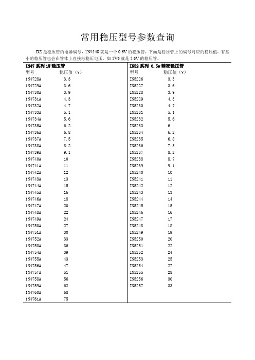
常用稳压型号参数查询DZ是稳压管的电器编号,1N4148就是一个0.6V的稳压管,下面是稳压管上的编号对应的稳压值,有些小的稳压管也会在管体上直接标稳压电压,如5V6就是5.6V的稳压管。
美标稳压二极管型号:HITACHI(日立):HITACHI(日立)0.5W稳压二极管型号参数稳压HZ3A1 2.5~2.7VHZ3A2 2.6~2.8VHZ3A3 2.6~2.9VHZ3B1 2.8~3.0VHZ3B2 2.9~3.1VHZ3B3 3.0~3.2V线性稳压器件(输入输出电流相等,压降3V以上)型号稳压(V) 最大输出电流可替代型号79L05 -5V 100mA79L06 -6V 100mA79L08 -8V 100mALM7805 5V 1A L7805,LM340T5 LM7806 6V 1A L7806LM7808 8V 1A L7808LM7809 9V 1A L7809LM7812 12V 1A L7812,LM340T12 LM7815 15V 1A L7815,LM340T15 LM7818 18V 1A L7815LM7824 24V 1A L7824LM7905 -5V 1A L7905LM7906 -6V 1A L7906,KA7906 LM7908 -8V 1A L7908LM7909 -9V 1A L7909LM7912 -12V 1A L7912LM7915 -15V 1A L7915LM7918 -18V 1A L7918LM7924 -24V 1A L792478L05 5V 100mA78L06 6V 100mA78L08 8V 100ma78L09 9V 100ma78L12 12V 100ma78L15 15V 100ma78L18 18V 100ma78L24 24V 100ma开关稳压器件(电压转换效率高)型号说明最大输出电流LM1575T-3.3 3.3V简易开关电源稳压器 1ALM1575T-5.0 5V简易开关电源稳压器 1A LM1575T-12 12V简易开关电源稳压器 1A LM1575T-15 15V简易开关电源稳压器 1A LM1575T-ADJ 简易开关电源稳压器(可调1.23V~37V) 1ALM1575HVT-3.3 3.3V简易开关电源稳压器 1A LM1575HVT-5.0 5V简易开关电源稳压器 1A LM1575HVT-12 12V简易开关电源稳压器 1ALM1575HVT-15 15V简易开关电源稳压器 1ALM1575HVT-ADJ 简易开关电源稳压器(可调1.23V~37V) 1ALM2575T-3.3 3.3V简易开关电源稳压器 1A LM2575T-5.0 5V简易开关电源稳压器 1A LM2575T-12 12V简易开关电源稳压器 1A LM2575T-15 15V简易开关电源稳压器 1A LM2575T-ADJ 简易开关电源稳压器(可调1.23V~ 37V) 1ALM2575HVT-3.3 3.3V简易开关电源稳压器 1A LM2575HVT-5.0 5V简易开关电源稳压器 1A LM2575HVT-12 12V简易开关电源稳压器 1A LM2575HVT-15 15V简易开关电源稳压器 1A LM2575HVT-ADJ 简易开关电源稳压器(可调1.23V~37V) 1A LM2576T-3.3 3.3V简易开关电源稳压器 3A LM2576T-5.0 5.0V简易开关电源稳压器 3A LM2576T-12 12V简易开关电源稳压器 3A LM2576T-15 15V简易开关电源稳压器 3A LM2576T-ADJ 简易开关电源稳压器(可调1.23V~37V) 3ALM2576HVT-3.3 3.3V简易开关电源稳压器 3A LM2576HVT-5.0 5.0V简易开关电源稳压器 3ALM2576HVT-12 12V简易开关电源稳压器 3ALM2576HVT-15 15V简易开关电源稳压器 3ALM2576HVT-ADJ 简易开关电源稳压器(可调1.23V~37V) 3A。
常用稳压管型号
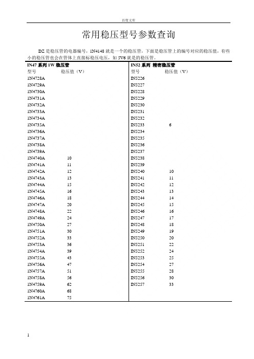
常用稳压型号参数查询DZ是稳压管的电器编号,1N4148就是一个的稳压管,下面是稳压管上的编号对应的稳压值,有些IN47系列1W稳压管型号稳压值(V)1N4728A1N4729A1N4730A1N4731A1N4732A1N4733A1N4734A1N4735A1N4736A1N4737A1N4738A1N4739A1N4740A 101N4741A 111N4742A 121N4743A 131N4744A 151N4745A 161N4746A 181N4747A 201N4748A 221N4749A 241N4750A 271N4751A 301N4752A 331N4753A 361N4754A 391N4755A 431N4756A 471N4757A 511N4758A 561N4759A 621N4760A 681N4761A 75 IN52系列精密稳压管型号稳压值(V)IN5226IN5227IN5228IN5229IN5230IN5231IN5232IN5233 6IN5234IN5235IN5236IN5237IN5238IN5239IN5240 10IN5241 11IN5242 12IN5243 13IN5244 14IN5245 15IN5246 16IN5247 17IN5248 18IN5249 19IN5250 20IN5251 22IN5252 24IN5253 25IN5254 27IN5255 28IN5256 30IN5257 33IN57~IN60系类精密性稳压管型号稳压值(V)IN5730IN5731IN5732IN5733IN5734IN5735IN5736 10IN5737 11IN5738 12IN5739 13IN5740 15IN5741 16IN5742 18IN5743 20IN5744 22IN5745 24IN5746 27IN5747 30IN5748 33IN5749 36IN5750 39IN5985IN5986IN5987 3IN5988IN5989IN5990IN5991IN5992IN5993IN5994IN5995IN5996IN5997IN5998IN5999IN6000 10IN6001 11IN6002 12IN6003 13IN6004 15IN6005 16IN6006 18 贴片型SOD-123穏压二极管型号规格型号稳压值(V)代码标示HZD5221B Z21HZD5222B Z22HZD5223B Z23HZD5224B Z24HZD5225B Z25HZD5226B Z26HZD5227B Z27HZD5228B Z28HZD5229B Z29HZD5230B Z30HZD5231B Z31HZD5232B Z32HZD5233B Z33HZD5234B Z34HZD5235B Z35HZD5236B Z36HZD5237B Z37HZD5238B Z38HZD5239B Z39HZD5240B 10V Z40 HZD5241B 11V Z41 HZD5242B 12V Z42 HZD5243B 13V Z43 HZD5244B 14V Z44IN6007 20 IN6008 22美标稳压二极管型号:500mW部分:型号稳压值(V)1N46141N4615 2V1N46161N46171N46181N4619 3V1N46201N46211N46221N46231N46241N46251N46261N46271N40991N41001N41011N41021N41031N4104 10V1N4105 11V1N4106 12V1N4107 13V1N4108 14V1N4109 15V1N4110 16V1N4111 17V1N4112 18V1N4113 19V1N4114 20V1N4115 22V1N4116 24V1N4117 25V1N4118 27V1N4119 28V1N4120 30V1N4121 33V1N4122 36V1N4123 39V1N4124 43V 1W稳压部分:型号稳压值(V)1N4727 3V01N4728 3V31N4729 3V61N4730 3V91N4731 4V31N4732 4V71N4733 5V11N4734 5V61N4735 6V21N4736 6V81N4737 7V51N4738 8V21N4739 9V11N4740 10V1N4741 11V1N4742 12V1N4743 13V1N4744 15V1N4745 16V1N4746 18V1N4747 20V1N4748 22V1N4749 24V1N4750 27V1N4751 30V1N4752 33V1N4753 36V1N4754 39V1N4755 43V1N4756 47V1N4757 51V1N4758 56V1N4759 62V1N4760 68V1N4761 75V1N4762 82V1N4763 91V1N4764 100V1N4125 47V1N4126 51V1N4127 56V1N4128 60V1N4129 62V1N4130 68V1N4131 75V1N4132 82V1N4133 87V1N4134 91V1N4135 100VHITACHI(日立):HITACHI(日立)稳压二极管型号参数稳压HZ3A1 ~HZ3A2 ~HZ3A3 ~HZ3B1 ~HZ3B2 ~HZ3B3 ~线性稳压器件(输入输出电流相等,压降3V以上)型号稳压(V) 最大输出电流可替代型号79L05 -5V 100mA79L06 -6V 100mA79L08 -8V 100mALM7805 5V 1A L7805,LM340T5 LM7806 6V 1A L7806LM7808 8V 1A L7808LM7809 9V 1A L7809LM7812 12V 1A L7812,LM340T12 LM7815 15V 1A L7815,LM340T15 LM7818 18V 1A L7815LM7824 24V 1A L7824LM7905 -5V 1A L7905LM7906 -6V 1A L7906,KA7906 LM7908 -8V 1A L7908LM7909 -9V 1A L7909LM7912 -12V 1A L7912LM7915 -15V 1A L7915LM7918 -18V 1A L7918LM7924 -24V 1A L792478L05 5V 100mA78L06 6V 100mA78L08 8V 100ma78L09 9V 100ma78L12 12V 100ma78L15 15V 100ma78L18 18V 100ma78L24 24V 100ma开关稳压器件(电压转换效率高)型号说明最大输出电流简易开关电源稳压器1A5V简易开关电源稳压器1ALM1575T-12 12V简易开关电源稳压器1ALM1575T-15 15V简易开关电源稳压器1ALM1575T-ADJ 简易开关电源稳压器(可调~37V) 1A 简易开关电源稳压器1A5V简易开关电源稳压器1ALM1575HVT-12 12V简易开关电源稳压器1ALM1575HVT-15 15V简易开关电源稳压器1ALM1575HVT-ADJ 简易开关电源稳压器(可调~37V) 1A简易开关电源稳压器1A5V简易开关电源稳压器1ALM2575T-12 12V简易开关电源稳压器1ALM2575T-15 15V简易开关电源稳压器1ALM2575T-ADJ 简易开关电源稳压器(可调~ 37V) 1A 简易开关电源稳压器1A5V简易开关电源稳压器1ALM2575HVT-12 12V简易开关电源稳压器1ALM2575HVT-15 15V简易开关电源稳压器1ALM2575HVT-ADJ 简易开关电源稳压器(可调~37V) 1A 简易开关电源稳压器3A简易开关电源稳压器3ALM2576T-12 12V简易开关电源稳压器3ALM2576T-15 15V简易开关电源稳压器3ALM2576T-ADJ 简易开关电源稳压器(可调~37V) 3A 简易开关电源稳压器3A简易开关电源稳压器3ALM2576HVT-12 12V简易开关电源稳压器3ALM2576HVT-15 15V简易开关电源稳压器3ALM2576HVT-ADJ 简易开关电源稳压器(可调~37V) 3A。
怎样判断l7805cv引脚各端口与引脚是否烧坏

怎样判断l7805cv引脚各端口与引脚是否烧坏
三端稳压集成电路lm7805。
电子产品中,常见的三端稳压集成电路有正电压输出的lm78 ***系列和负电压输出的lm79***系列。
顾名思义,三端IC是指这种稳压用的集成电路,只有三条引脚输出,分别是输入端、接地端和输出端。
它的样子象是普通的三极管,TO- 220 的标准封装,也有lm9013样子的TO-92封装。
l7805 引脚图
l7805 是我们最常用到的稳压芯片了,他的使用方便,用很简单的电路即可以输入一个直流稳压电源,他的输出电压恰好为5v,刚好是51系列单片机运行所需的电压,他有很多的系列如ka7805,ads7805,cw7805 等,性能有微小的差别,用的最多的还是Im7805,下面我简单的介绍一下他的3 个引脚以及用它来构成的稳压电路的资料。
7805 引脚图。
- 1、下载文档前请自行甄别文档内容的完整性,平台不提供额外的编辑、内容补充、找答案等附加服务。
- 2、"仅部分预览"的文档,不可在线预览部分如存在完整性等问题,可反馈申请退款(可完整预览的文档不适用该条件!)。
- 3、如文档侵犯您的权益,请联系客服反馈,我们会尽快为您处理(人工客服工作时间:9:00-18:30)。
L7805 L7805
S h e nzhhettnp:H&//toomr Co.Ltd
5/6
L7805
特性曲线:
L7805
L7805
S he n z hh ettnp:H&//toomr Co.Ltd
6/6
参数名称
输出电压
线性调整率*
负载调整率* 静态电流 静态电流改变 输出电压漂移 输出噪声电压 纹波抑制 漏电压 输出电阻 短路电流 峰值电流
符号
测试条件
Vo Regline Regload
TJ=+25°C
5.0mA≤ Io≤ 1.0A,Po≤ 15W Vi=7V to 20V
TJ=+25°C
Vi=7V to 25V Io=500mA Vi=8V to 12V Io=1.2A
L7805
Shenzhen H&M Semiconductor Co.Ltd http://
3/6
L7805
L7805
L7805
L7805
Shenzhen H&M Semiconductor Co.Ltd
http://
4/6
L7805
L7805
TJ=+25°C
Io=5.0mA to 1.5A Io=250mA to 750mA
IQ
TJ=+25°C
Δ IQ
Io=5.0mA to 1.0A Vi=7V to 25V
Δ Vo/Δ T Io=5.0mA
VN
f=10R f= 120Hz Vi= 8V to 18V
热阻
工作工作范围 贮存温度范围
符号 Vi
Rθ JC Rθ JA TOPR TSTG
数值 35 5 65
0~+125 -65~+150
单位 V
°C/W °C/W
°C °C
电特性:
(若 无 其 它 规 定 : 0°C< TJ < 1 2 5 °C , Vi=10V,Ci=0.33μ F,Co = 0 .1 μ F)
最大 单位
5.2 V
5.25
50 mV
25
50 mV
25 8.0 mA 0.5
mA 1.0
mV/°C
μ V / Vo dB V mΩ mA A
Shenzhen H&M Semiconductor Co.Ltd
http://
2/6
应用图:
L7805
L7805
L7805
L7805
封装外形图:
L7805
主要特点:
固定输出电压 :5V 内置短路保护电路 内置热保护电路 输出晶体管安全工作区保护电路
功能框图:
Shenzhen H&M Semiconductor Co.Ltd
http://
1/6
L7805
极 限 值 : (Ta= 25°C)
输入电压
参数名称
V D r o p I =o 1 . 2 A , T J = + 2 5 ° C r O =f 1 K H z
I S C = Vi 3 5 V, T J = + 2 5 ° C
IPK
TJ=+25°C
最小 典型 4.8 5.0 4.75 5.0
4.0 1.6 9 4 5.0 0.03 0.3 -0.8 42 62 73 2 15 230 2.2
1.2A 三端正电源稳压电路 L7805
概述:
L7805是 一 块 三 端 正 电 源 稳 压 集 成 电 路。该电路内置短路保护及热保护电路, 具有输出电压固定的特点,广泛应用于各 种电视机、收录机、电子仪器等设备中作 电源稳压用。
L7805采 用 三 引 线 带 散 热 片 塑 料 TO-220的 封 装 形 式 封 装 。