化学气相沉积中输运现象的研究
cvd化学气相沉积原理碳化硅

cvd化学气相沉积原理碳化硅
化学气相沉积(CVD)是一种重要的化学气相沉积技术,用于在固体表面上沉积薄膜或纳米结构材料。
碳化硅(SiC)是一种重要的半导体材料,具有优异的热学性能和电学性能,因此在CVD中碳化硅的沉积具有重要的应用价值。
CVD碳化硅的原理主要包括以下几个方面:
1. 反应物气体输运,在CVD过程中,通常会使用一种或多种气体作为反应物,例如硅源气体(如硅烷SiH4)和碳源气体(如甲烷CH4)。
这些气体通过输运系统输送到反应室中。
2. 反应室条件控制,在反应室中,通过控制温度、压力和气体流量等参数,创造出适合碳化硅沉积的环境。
通常情况下,需要高温(约1200-1600°C)和较高的气压来促进碳化硅的生长。
3. 化学反应,碳源气体和硅源气体在反应室中发生化学反应,生成碳化硅薄膜。
反应机理主要包括热解和气相反应两种方式。
在热解过程中,碳源气体分解生成碳原子,与硅源气体反应形成碳化硅;在气相反应过程中,碳源气体和硅源气体直接在气相中反应生
成碳化硅。
4. 沉积控制,通过控制反应条件和沉积时间,可以控制碳化硅薄膜的厚度、结晶度和取向等性质。
总的来说,CVD碳化硅的原理是通过控制适当的反应条件和气体输送,使得碳源气体和硅源气体在反应室中发生化学反应,从而在固体表面沉积出碳化硅薄膜。
这种技术在半导体器件、光电子器件等领域具有重要的应用前景。
等离子体增强化学气相沉积(二)2024

等离子体增强化学气相沉积(二)引言概述:等离子体增强化学气相沉积(PECVD)是一种广泛应用于微电子和薄膜制备领域的表面改性技术。
本文将探讨PECVD的工作原理和应用,着重介绍其在材料科学和纳米技术领域的应用。
文中将从五个方面进行阐述:等离子体的产生、反应区中化学物质激发、气体输运机制、薄膜沉积过程和应用案例。
正文:一、等离子体的产生1. 等离子体的定义和特点2. 等离子体的产生方法3. 等离子体源的种类和选择4. 等离子体源的作用机制5. 等离子体温度和密度的控制方法二、反应区中化学物质激发1. 等离子体激发的基本原理2. 等离子体激发对反应的影响3. 等离子体激发的参数优化4. 等离子体激发对沉积薄膜性能的影响5. 等离子体激发的技术进展和挑战三、气体输运机制1. 气体输运的基本原理2. 气体输运的控制方法3. 气体输运对沉积速率和成分的影响4. 气体输运对薄膜质量的影响5. 气体输运在PECVD中的应用案例四、薄膜沉积过程1. 沉积过程概述和反应动力学2. 主要影响沉积过程的因素3. 沉积速率的控制方法4. 沉积过程中的界面反应和成核机制5. 沉积薄膜的表征和评估方法五、应用案例1. 硅基和非硅基薄膜的沉积2. 光学薄膜和光学器件的制备3. 氢化非晶硅薄膜的应用4. 生物材料和生物传感器的制备5. 纳米材料和纳米器件的制备结论:等离子体增强化学气相沉积是一种广泛应用于微电子和薄膜制备领域的表面改性技术。
本文从等离子体的产生、反应区中化学物质激发、气体输运机制、薄膜沉积过程和应用案例五个方面进行了详细阐述。
通过深入了解PECVD的工作原理和应用,我们可以更好地利用这一技术来满足各种材料科学和纳米技术的需求。
第四章--薄膜的化学气相沉积
LB膜可分三类:
已 经 被 物 理 吸 附 分 子 所占 据 的 比 例 。
32
(五)表面扩散
薄膜表面吸附的分子或原子也具有一定的扩 散能力,这也是薄膜结构与性能会产生巨大 差异的原因。
在薄膜表面,被吸附的分子和原子一般应处 于能量较低的势阱中。因此,吸附分子、原 子的扩散也需要克服相应的能垒Es。
33
单位表面上吸附分子、原子发生扩散的 速率为
27
(四)表面吸附及表面化学反应
气体组分在扩散至薄膜表面后,还要经 过表面吸附、表面扩散、表面反应、反 应产物脱附等多个过程,才能完成薄膜 的沉积过程。
吸附、反应、脱附过程的快慢也可能会 成为薄膜沉积过程的控制性环节 。
28
29
气相组分向衬底表面的扩散通量为J;到 达衬底后被衬底表面俘获得几率为δ;被 反射离开衬底表面的几率为1- δ;
Es
Dt e 2RT
上式表明,表面吸附分子、原子的扩散能力 随着温度的上升呈指数形式增加。
表面分子、原子的平均扩散距离随温度的变 化具体如何?
36
划分为沉积机制为主温度区间和脱附机 制为主的温度区间
37
(六)温度对CVD过程中薄膜沉积速 率的影响
温度是化学气相沉积过程中最重要的参数之 一。
例如下述反应
A=B+C
的正向反应进程只涉及组元A的行为
19
一 级 反 应 的 反 应 速 率 等于
R
knA
k
pA kT
(4- 41)
式
中
,k
为
反
应
的
速
度
常
数
;
n A、p A分 别 为 气 体 组 元A的 体 密 度 和 分 压 ;
化学气相沉积技术在材料制备中的应用

化学气相沉积技术在材料制备中的应用随着时代的进步和科技的不断发展,新材料的研发和应用逐渐成为了人们关注的焦点。
而其中,化学气相沉积技术作为一种常见的材料制备技术,其应用已经被广泛开展。
本文将对化学气相沉积技术的概念、原理、种类以及应用进行介绍。
一、概念化学气相沉积技术又称为化学气相沉积法 (Chemical Vapor Deposition, CVD),是利用热力学原理在气相中进行的一种新型制备材料技术。
在化学气相沉积过程中,通常由液体或固体的前驱体在高温下气相化并分解,在特定条件下选择与基底反应,最终在基底上形成所需的材料。
二、原理化学气相沉积技术的基本原理就是利用化学反应产生气体或气相的化学物质,通过气相输运将化合物输送到基底表面上,并在相应的条件下化学反应沉积,直至形成所需材料。
三、种类根据化学反应方式,化学气相沉积技术可分为以下几种类型。
1. 热CVD (Thermal CVD)热CVD主要利用高温条件下有机气相物质的热解产生的自由基进行反应。
应用最为广泛的化学气相沉积技术便是热CVD,其应硅系材料、碳纤维、SiC等领域都有应用。
2. 电化学气相沉积 (Electrochemical Vapor Deposition, ECVD)电化学气相沉积是在气相条件下,在电化学活性气体环境中导入外部电流对挥发性前驱体进行电化学氧化反应而实现沉积。
3. 等离子体CVD (Plasma CVD)等离子体CVD是在非平衡等离子体中激发基底表面上的反应物分子,并以氢原子、氮原子等作为活性物种进行反应。
应用于反应物分子之间交联或解离反应等复杂反应过程。
4. 压力化学气相沉积 (Pressure-CVD)压力化学气相沉积技术主要依靠反应物在高压下进行反应,与临界点处的物质相变及其相应物理学特性密切相关。
四、应用化学气相沉积技术有效地解决了传统的材料制备技术所固有的限制,并被广泛应用于材料制备、能源储存等领域。
气相沉积原理

气相沉积原理气相沉积(CVD)是一种重要的薄膜制备技术,广泛应用于半导体、光电子、纳米材料等领域。
其原理是通过在高温下将气体中的化合物分解或反应,使其沉积在基底表面上,形成薄膜或涂层。
气相沉积技术具有高纯度、均匀性好、厚度可控等优点,因此受到了广泛的关注和应用。
气相沉积原理的核心是气体中的化合物在高温下发生化学反应,生成固体产物并沉积在基底表面上。
这一过程主要包括气体输运、表面吸附、化学反应和沉积四个基本步骤。
首先,气体通过输运系统输送到反应室中,然后在基底表面发生吸附,形成反应物质的吸附层。
接着,在高温条件下,吸附层中的化合物发生化学反应,生成固体产物并沉积在基底表面上。
最后,通过控制气体输送和反应条件,可以实现对薄膜厚度、成分和结构的精确控制。
气相沉积技术主要分为化学气相沉积(CVD)和物理气相沉积(PVD)两种类型。
其中,CVD是指在高温条件下,气体中的化合物发生化学反应并沉积在基底表面上,形成薄膜或涂层。
而PVD则是通过物理手段,如溅射、蒸发等,将固体材料沉积在基底表面上。
相比之下,CVD技术可以实现更高的纯度和均匀性,因此在半导体、光电子等领域得到了广泛的应用。
在实际应用中,气相沉积技术需要考虑多个因素,如反应气体的选择、反应温度、压力、基底表面状态等。
不同的反应条件会影响薄膜的成分、结构和性能,因此需要精确控制这些参数。
此外,还需要考虑反应室的设计、气体输送系统、基底表面处理等方面的问题,以确保薄膜的质量和稳定性。
总的来说,气相沉积技术是一种重要的薄膜制备技术,具有高纯度、均匀性好、厚度可控等优点,因此在半导体、光电子、纳米材料等领域得到了广泛的应用。
通过精确控制反应条件和参数,可以实现对薄膜的精确控制,满足不同领域的需求。
随着科学技术的不断发展,相信气相沉积技术在未来会有更广阔的应用前景。
化学气相沉积的基本过程
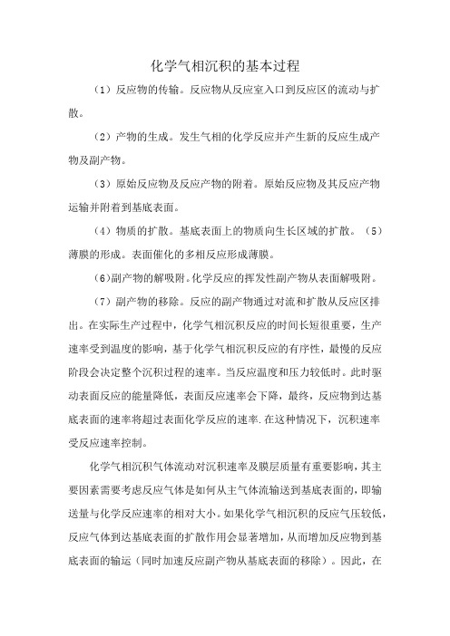
化学气相沉积的基本过程
(1)反应物的传输。
反应物从反应室入口到反应区的流动与扩散。
(2)产物的生成。
发生气相的化学反应并产生新的反应生成产
物及副产物。
(3)原始反应物及反应产物的附着。
原始反应物及其反应产物
运输并附着到基底表面。
(4)物质的扩散。
基底表面上的物质向生长区域的扩散。
(5)薄膜的形成。
表面催化的多相反应形成薄膜。
(6)副产物的解吸附。
化学反应的挥发性副产物从表面解吸附。
(7)副产物的移除。
反应的副产物通过对流和扩散从反应区排出。
在实际生产过程中,化学气相沉积反应的时间长短很重要,生产速率受到温度的影响,基于化学气相沉积反应的有序性,最慢的反应阶段会决定整个沉积过程的速率。
当反应温度和压力较低时。
此时驱动表面反应的能量降低,表面反应速率会下降,最终,反应物到达基底表面的速率将超过表面化学反应的速率.在这种情况下,沉积速率
受反应速率控制。
化学气相沉积气体流动对沉积速率及膜层质量有重要影响,其主要因素需要考虑反应气体是如何从主气体流输送到基底表面的,即输送量与化学反应速率的相对大小。
如果化学气相沉积的反应气压较低,反应气体到达基底表面的扩散作用会显著增加,从而增加反应物到基底表面的输运(同时加速反应副产物从基底表面的移除)。
因此,在
实际的化学气相沉积工艺中多采用低压化学气相沉积(LPCVD),而较少采用常压化学气相沉积(APCVD)。
化学气相沉积

Chemical Vapor Deposition
本章主要内容
化学气相沉积的基本情况 化学气相沉积的化学反应类型 化学气相沉积的热力学计算 气体输运与薄膜生长 化学气相沉积方法 CVD形成薄膜时所利用的化学反应 及其在IC中的功能
化学气相沉积的基本情况
化学气相沉积的基本情况-化
学气相沉积定义
–化学成分比例条件 (mol比例):
•化学反应热力学平衡常数计算
平衡常数K数值的大小是反应进行程度的标志。因为平衡状态是反应进行的最大 限度,而平衡常数的表达式很好的表示出了在反应达到平衡时的生成物和反应 物的浓度关系,一个反应的平衡常数越大,说明反应物的平衡转化率越高
平衡常数K的意义
∑ vB 压力平衡常数K P = K (1/ P ) Φ Φ − ∑ vB 浓度平衡常数K N = K ( P / P )
热力学计算的目的及其复杂性: •预测化学反应进行的可能性;提供化学反应的平衡点位 置;了解工艺参数对平衡点的影响; •热力学计算必须包括实际化学反应过程中所涉及的所有 化学反应; 单晶硅薄膜生长:Si-Cl-H系统,固态Si活度1 •化学反应热力学方程
化学反应热力学方程(续)
化学反应条件方程
–气体压强条件:
等离子体增强CVD(PECVD)
基于CVD的薄膜生长方法 其它薄膜外延方法
大气压化学气相 沉积(APCVD)
高温大气压CVD: •炉体:冷壁型/热壁型 •炉壁加热方式:射频加热/辐 射加热 •样品放置:倾斜/平置 •特点:简单经济、稳定高效; 腐蚀、污染、耗能; •应用:外延Si薄膜制备、TiN, TiC等超硬涂层等
气体输运与薄膜生长- CVD的动力学范围
当淀积发生于质量传输控制区域时(高温),淀积速 率与温度的关系是相对不变的,硅片上的气体流量和 反应剂向硅片表面的传输是十分重要的,它会对设备 结构和硅片放置设置主要限制,例如,硅外延淀积, 气相过程是主要的 当淀积发生于表面反应控制区域时(低温),这个过 程对温度十分敏感,导致对气流和硅片放置的限制比 较少,例如,多晶硅填充,淀积对温度非常敏感
二维MoS2薄膜的可控制备及其电子输运特性研究
二维MoS2薄膜的可控制备及其电子输运特性研究【摘要】二维MoS2作为一种新型半导体材料,在电子学和光电子学领域具有广泛的应用前景。
在本文研究中,我们采用化学气相沉积(CVD)技术在氧化硅基底上制备了高质量的二维MoS2薄膜,并通过压电传感器进行了表征。
通过在不同条件下控制CVD过程中的温度、气体流量和反应时间等参数,成功地实现了对MoS2薄膜的可控制备。
同时,利用离子束雕刻技术对MoS2薄膜进行了纳米加工,使其形成了具有排列有序的长条纹的结构,可作为电极进行电子输运特性研究。
进一步的电子输运实验表明,MoS2薄膜具有半导体特性,并在室温下呈现出n型导电性。
在不同温度和电场的情况下,MoS2薄膜的电子输运性质表现出明显的变化。
通过调控材料的缺陷和掺杂,成功地实现了对MoS2薄膜电子输运特性的调控。
结果表明,MoS2薄膜在电子学和光电子学器件中具有广泛的应用前途。
【关键词】二维MoS2;CVD;可控制备;纳米加工;电子输运特性【Abstract】Two-dimensional (2D) MoS2 as a novel semiconductor material has great potential applications in thefields of electronics and optoelectronics. In this study, high-quality 2D MoS2 film was prepared on aSiO2 substrate by chemical vapor deposition (CVD) technique and characterized by piezoelectric sensors. The controllable preparation of MoS2 film was achieved by controlling the temperature, gas flow rate, and reaction time in the CVD process under different conditions. Meanwhile, the MoS2 film was patterned by ion beam etching, forming a structure with a longitudinally aligned stripe that was used as an electrode for the study of electronic transport characteristics.Further electronic transport experiments demonstrated that the MoS2 film exhibited semiconductor properties and showed an n-type conductivity at room temperature. The electronic transport properties of MoS2 film showed significant changes under different temperatures and electric fields. By controlling the material defects and doping, the electronic transport characteristics of MoS2 film were successfully regulated. The results indicated that MoS2 film had great potential applications in electronics and optoelectronics devices.【Keywords】Two-dimensional MoS2; CVD; Controllable preparation; Nanofabrication; Electronic transport characteristicTwo-dimensional MoS2 has attracted increasingattention in recent years due to its unique properties and potential applications in electronics and optoelectronics devices. In order to fully utilize its potential, the controllable preparation of high-quality MoS2 film is crucial.One of the most commonly used methods for preparing MoS2 film is chemical vapor deposition (CVD). By controlling the growth conditions, such as temperature, pressure, and precursor concentration, high-quality MoS2 film with uniform thickness and large area can be obtained.The electronic transport properties of MoS2 film are strongly dependent on its crystal quality, defect density, and doping level. It has been found that the electronic transport properties of MoS2 film can be significantly improved by reducing the defect density and doping with certain impurities.Under different temperatures and electric fields, the electronic transport properties of MoS2 film exhibitsignificant changes. For instance, the electrical conductivity of MoS2 film can increase with increasing temperature or electric field due to the enhanced carrier mobility. Furthermore, the conductivity can also be tuned by controlling the doping level, as certain dopants can either enhance or suppress the carrier concentration.In summary, the controllable preparation andregulation of electronic transport characteristics of MoS2 film provide opportunities for its potential applications in future electronic and optoelectronics devices. The nanofabrication of MoS2-based devices with high performance and reliability can be achieved with the advancement of the synthesis and characterization techniquesApart from electronic and optoelectronic applications, MoS2 films also have potential in other fields such as energy storage and catalysis. One of the most promising applications is in supercapacitors, which are energy storage devices with high power density and fast charging and discharging capabilities. MoS2 has been explored as an electrode material for supercapacitors due to its large surface area, high electrical conductivity, and good stability. Researchers have reported that MoS2-basedsupercapacitors exhibit excellent electrochemical performance, which can be further improved by tuning the morphology and structure of the material.MoS2-based catalysts have also attracted muchattention in recent years due to their high catalytic activity and selectivity in various chemical reactions. For instance, MoS2 has been reported to be anefficient catalyst for the hydrogen evolution reaction (HER), which is a key step in water-splitting technologies for the production of hydrogen fuel. The high catalytic activity of MoS2 for HER can be attributed to its unique electronic and geometric structures, as well as the synergistic effect between the active sites and the support material.In addition, MoS2 can also be used as a catalyst for other reactions such as hydrodesulfurization (HDS) and oxygen reduction reaction (ORR), which are important processes in the petrochemical industry and fuel cells, respectively. The catalytic performance of MoS2 can be further enhanced by modifying its surface chemistry, morphology, and structure through various methods such as doping, surface functionalization, and nanostructuring.Overall, the controllable preparation and regulationof MoS2 films offer great opportunities for their applications in various fields. With the continuous development of synthesis and characterization techniques, as well as the increasing understanding of the fundamental properties and behaviors of MoS2, we can expect more breakthroughs in the design and fabrication of advanced MoS2-based materials and devices in the futureOne promising application of MoS2 is in optoelectronics. Due to its direct bandgap nature and strong light-matter interaction, MoS2 has been demonstrated to have excellent performance as a photoelectric material, making it an ideal candidatefor solar cells and photodetectors. Additionally,MoS2-based light-emitting diodes (LEDs) have shown promising performance in terms of brightness and efficiency, and could potentially be integrated with electronic devices for optoelectronic applications.Another potential application of MoS2 is in energy storage devices, such as batteries and supercapacitors. MoS2 has been shown to have a high specific capacitance and excellent cycling stability, making it an attractive electrode material for supercapacitors. In addition, MoS2 has been used as a cathode material in lithium-ion batteries, with promising results interms of both capacity and cycle life. Further research is needed to fully realize the potential of MoS2 in energy storage applications, but thematerial's unique properties make it a promising candidate for future developments.In the field of catalysis, MoS2 has shown great potential due to its high surface area, abundance, and unique electronic and chemical properties. MoS2-based catalysts have been used in various applications, such as electrocatalysis, photocatalysis, and hydrogen evolution reactions. Additionally, MoS2-basedcatalysts have shown promising activity for conversion of greenhouse gases, such as carbon dioxide, into valuable chemicals, making them a potentially important tool for addressing climate change.Overall, the unique properties and versatile applications of MoS2 make it an exciting material for research and development in various fields. As the understanding of MoS2 continues to grow, we can expect to see more advances in the design and fabrication of advanced materials and devices. The development of new synthesis and characterization techniques will also play a critical role in unlocking the full potential of MoS2-based materials. Ultimately, these advancements have the potential to revolutionize anumber of industries and make a significant impact on our daily livesIn conclusion, MoS2 is a promising material that has garnered significant attention due to its unique properties and potential applications in various fields. The research and development in this area are expected to lead to significant advancements in the design and fabrication of advanced materials and devices, which could revolutionize numerous industries and make a significant impact on our daily lives. Continued efforts in the development of new synthesis and characterization techniques are critical to unlocking the full potential of MoS2-based materials。
- 1、下载文档前请自行甄别文档内容的完整性,平台不提供额外的编辑、内容补充、找答案等附加服务。
- 2、"仅部分预览"的文档,不可在线预览部分如存在完整性等问题,可反馈申请退款(可完整预览的文档不适用该条件!)。
- 3、如文档侵犯您的权益,请联系客服反馈,我们会尽快为您处理(人工客服工作时间:9:00-18:30)。
学 出版社,1 7 . 97
[】T E T T A P 3 E R S R ,YO A V NOV C M. a t a Mo en I H M Anl i l d l g yc i
o Na rl o vci o zna A n l R . A a e, f t aC n et ni H r o tl n ui【 】 AI A Pp r u o n i
中图分类号 :T 2 .1 Q021 文献标志码 :A 文章编号 :10 -692 0)60 2 .5 0 213 (0 80.020
Th s a c f a s o tP e o n eRe e r h o n p r h n me ai CVD Tr n
WA NG O b n GU . i
tpc l y ia CVD a tr f o z n l dv ria. T ercruain whc fu n e ytes a eo ra tr tmp rtr f U v lct r co s h r o t etc 1 h ic lt , e o i aa n e o ihi il e c db p f e co, e eaueo wa , eo i sn h h y
化 学气相 沉积,简称 C VD ( h m c l a o p s C e ia V p r oi De -
C D 中的输运现象 是指 C V VD 反应器 中的热量 、质
t n ,可 生长单晶和多 晶薄膜,广泛用 于微 电子器件 、 i ) o
光 电器件 以及表面工程,是制备功能材料 、结构材料和
收稿 日期 :20 -81;修 回 日期 :2 0-00 0 8 ・2 0 0 81-5
基金项 目 :国家 自然 科学基 金资助 项 目 (0 706 636 0 ) 作者简 介 :王国斌 (93 ) 男,江苏苏 州人 ,硕 士研 究生 ,主 要 18一 , 研究 方 向:晶体 生长 中的传 热传质 .
模拟分析应用于 实际情况是 目前最为经济和快速的方法。 由此, 通过计算机模 拟手段对 C VD中的输运现象进行深 入了解就显得尤为重要 了。 本文将介绍 C D反应器 中输 V
运现象的模拟研究进展,重点 阐述传统 的水平式和垂直 式反应器 中的混合对流及其影响 因素。
【 索科洛夫 H 津格乐. 2 】 M 喷射器 [ . M】 黄秋云,译. 北京:科
2 0 : 9 9 05 5.
H r o tlC l d clA n l J. . etTa s r 17 , o zn yi r a n ui【】 J H a rnf , 8 i a ni e 9
量和动量的传输, 即传热 、传质及流体 流动 。研究反应
器 内的输运现象主要有 两方面原 因[: 2 ①只有当输运到衬
纳米 材料 的最 重要 的方法…。在 化学 气相沉积 过程 中, 反应气体 ( SH ,Ga( H ) +NH )从气源引入反 如 i4 C 33 3 应腔,利用加热 、等 离子体 或激光 等引发化学反应,从
热 能 工 程
工业加热 第 3 7卷20 年第 6 08 期
化学气相沉积中输运现象的研究
王 国斌
( 江苏大学 能源与动力工程学 院,江苏 镇江 221) 10 3
摘要 :对化学气相沉积 ( V C D)中输运现象的研究进行 了总结 。重点阐述 了典型的水 平式和垂直式 C VD反应器 中混合对 流的模拟 结果,以及反应器几何形状 、壁面温度 、流体流速、压强 、浓度梯度等 因素对其的影响。 关键词:C D;输运现象 ;混合对流 ;传热传质 ;模拟 V
( co l f n ryadP we E gn e n , i guUnvr t h  ̄i g 2 2 1,C ia Sh o E eg o r n ier g Ja s iesy o n i n i ,Z e a 103 hn ) n
Ab t a t h e e r h s f mn p a p e o n s r c :T er s a c e t s o h n me a i CVD a es mma z d Th x dr cr u a i ni il h we i i l t n i e o n r u i re. emie ic lt ma n y s o d v asmu ai t e o s o nh
要的意义。 虽然利用实验 已观测到众多输运现象,但对很多实 际 C D系统 来说,由于光学路径 的实际限制以及有可能 V 对反应器造成污染,直接观测流动现象是很 困难的。而
等 )( 1。 图 )
加热器
o o o
利用计算机数值模拟,能有效节约时间与成本 。所以将
图1 C VD工作示意图[
而在加热的基片表面生长单 晶或多 晶薄膜 ( S,G N 如 i a
底各部位的反应粒子及掺杂粒子数量都相等时 ,才能满
足组分和掺杂均匀性 的要求,故必须在沉积表面提供一 个稳定的,无涡旋 的,均匀 的气 流;② 为达到满意的生 长速率,必须有足够量的反应粒子到达生长表面,故必 须保证反应产物的传质速率 。 因此 ,深入 了解反应器 内 部的输运过程,对控制薄膜 的生长速率和质量具有很重