BCB1012UH-F00;中文规格书,Datasheet资料
BUK130-50DL,118;中文规格书,Datasheet资料

Philips Semiconductors Product specificationLogic level TOPFETBUK130-50DLSMD version of BUK119-50DLDESCRIPTIONQUICK REFERENCE DATAMonolithic temperature andSYMBOL PARAMETERMAX.UNIT overload protected logic level power MOSFET in TOPFET2 technology V DS Continuous drain source voltage 50V assembled in a 3 pin surface mount I D Continuous drain current 20A plastic package.P D Total power dissipation90W T jContinuous junction temperature 150˚C APPLICATIONSR DS(ON)Drain-source on-state resistance 28m ΩI ISLInput supply currentV IS = 5 V650µAlamps motors solenoids heatersapplications.FEATURESTrenchMOS output stage Current limitingOverload protectionOvertemperature protectionProtection latched reset by input 5 V logic compatible input level Control of output stage and supply of overload protection circuits derived from input Low operating input current permits direct drive by micro-controllerESD protection on all pins Overvoltage clamping for turn off of inductive loadsPINNING - SOT404PIN CONFIGURATIONSYMBOLPhilips Semiconductors Product specification Logic level TOPFET BUK130-50DL SMD version of BUK119-50DLLIMITING VALUESLimiting values in accordance with the Absolute Maximum Rating System (IEC 134)SYMBOL PARAMETER CONDITIONS MIN.MAX.UNITVDSContinuous drain source voltage1-50VI D Continuous drain current VIS= 5 V; Tmb=25˚C-self -AlimitedI D Continuous drain current VIS= 5 V; Tmb ≤121˚C-20AIIContinuous input current-55mAIIRMRepetitive peak input currentδ≤ 0.1, tp = 300 µs-5050mAPD Total power dissipation Tmb≤ 25˚C-90WTstgStorage temperature-55175˚CTjContinuous junction temperature2normal operation-150˚CTsoldCase temperature during soldering-260˚C ESD LIMITING VALUESYMBOL PARAMETER CONDITIONS MIN.MAX.UNITVCElectrostatic discharge capacitor Human body model;-2kVvoltage C = 250 pF; R = 1.5 kΩOVERVOLTAGE CLAMPING LIMITING VALUESAt a drain source voltage above 50 V the power MOSFET is actively turned on to clamp overvoltage transients. SYMBOL PARAMETER CONDITIONS MIN.MAX.UNITInductive load turn-off IDM = 20 A; VDD≤ 20 VEDSM Non-repetitive clamping energy Tmb≤ 25˚C-350mJEDRM Repetitive clamping energy Tmb≤ 95˚C; f = 250 Hz-45mJOVERLOAD PROTECTION LIMITING VALUEWith an adequate protection supply provided via the input pin, TOPFET can protect itself from two types of overload - overtemperature and short circuit load.SYMBOL PARAMETER REQUIRED CONDITION MIN.MAX.UNITVDS Drain source voltage3 4 V ≤ VIS≤ 5.5 V035VTHERMAL CHARACTERISTICSSYMBOL PARAMETER CONDITIONS MIN.TYP.MAX.UNITThermal resistanceRth j-mbJunction to mounting base-- 1.25 1.39K/WRth j-aJunction to ambient minimum footprint FR4 PCB-50-K/W 1 Prior to the onset of overvoltage clamping. For voltages above this value, safe operation is limited by the overvoltage clamping energy.2 A higher Tj is allowed as an overload condition but at the threshold Tj(TO)the over temperature trip operates to protect the switch.3 All control logic and protection functions are disabled during conduction of the source drain diode.Philips Semiconductors Product specification Logic level TOPFET BUK130-50DL SMD version of BUK119-50DLOUTPUT CHARACTERISTICSLimits are for -40˚C ≤ Tmb ≤ 150˚C; typicals are for Tmb= 25˚C unless otherwise specifiedSYMBOL PARAMETER CONDITIONS MIN.TYP.MAX.UNIT Off-state VIS= 0 VV(CL)DSS Drain-source clamping voltage ID= 10 mA50--VIDM= 4 A; tp≤ 300 µs; δ≤ 0.01506070VI DSS Drain source leakage current VDS= 40 V--100µATmb= 25˚C-0.110µAOn-state VIS≥ 4.4 V; tp≤ 300 µs; δ≤ 0.01RDS(ON)Drain-source resistance IDM= 10 A--52mΩTmb= 25˚C-2228mΩOVERLOAD CHARACTERISTICSVIS = 5 V; Tmb= 25˚C unless otherwise specified.SYMBOL PARAMETER CONDITIONS MIN.TYP.MAX.UNIT Short circuit loadI D Drain current limiting VDS= 13 V28.54357A4.4 V ≤ VIS≤ 5.5 V;21-65A-40˚C ≤ Tmb≤ 150˚COverload protectionPD(TO)Overload power threshold device trips if PD> PD(TO)75185250WTDSCCharacteristic time which determines trip time1200380600µsOvertemperature protectionTj(TO)Threshold junction150170-˚C temperature21 Trip time td sc varies with overload dissipation PDaccording to the formula td sc≈ TDSC/ ln[ PD/ PD(TO)].2 This is independent of the dV/dt of input voltage VIS.Philips Semiconductors Product specification Logic level TOPFET BUK130-50DL SMD version of BUK119-50DLINPUT CHARACTERISTICSThe supply for the logic and overload protection is taken from the input.Limits are for -40˚C ≤ Tmb ≤ 150˚C; typicals are for Tmb= 25˚C unless otherwise specifiedSYMBOL PARAMETER CONDITIONS MIN.TYP.MAX.UNITVIS(TO)Input threshold voltage VDS= 5 V; ID= 1 mA0.6- 2.4VTmb= 25˚C 1.1 1.6 2.1VI IS Input supply current normal operation; VIS= 5 V100220400µAVIS= 4 V80195330µAI ISL Input supply current protection latched; VIS= 5 V200400650µAVIS= 3 V130250430µAVISR Protection reset voltage1reset time tr≥ 100 µs 1.52 2.9Vt lr Latch reset time VIS1= 5 V, VIS2< 1 V1040100µsV(CL)IS Input clamping voltage II= 1.5 mA 5.5-8.5VRIG Input series resistance2Tmb= 25˚C-33-kΩto gate of power MOSFETSWITCHING CHARACTERISTICST mb = 25˚C; VDD= 13 V; resistive load RL= 4 Ω. Refer to waveform figure and test circuit.SYMBOL PARAMETER CONDITIONS MIN.TYP.MAX.UNITtd on Turn-on delay time VIS= 5 V-2550µstrRise time-50100µstd off Turn-off delay time VIS= 0 V-60120µstfFall time-50100µs1 The input voltage below which the overload protection circuits will be reset.2 Not directly measureable from device terminals.Philips Semiconductors Product specificationLogic level TOPFETBUK130-50DLSMD version of BUK119-50DLMECHANICAL DATA1 Epoxy meets UL94 V0 at 1/8". Net mass: 1.4 gFor soldering guidelines and SMD footprint design, please refer to Data Handbook SC18.Philips Semiconductors Product specification Logic level TOPFET BUK130-50DL SMD version of BUK119-50DLDEFINITIONSDATA SHEET STATUSDATA SHEET PRODUCT DEFINITIONSSTATUS1STATUS2Objective data Development This data sheet contains data from the objective specification forproduct development. Philips Semiconductors reserves the right tochange the specification in any manner without noticePreliminary data Qualification This data sheet contains data from the preliminary specification.Supplementary data will be published at a later date. PhilipsSemiconductors reserves the right to change the specification withoutnotice, in ordere to improve the design and supply the best possibleproductProduct data Production This data sheet contains data from the product specification. PhilipsSemiconductors reserves the right to make changes at any time inorder to improve the design, manufacturing and supply. Changes willbe communicated according to the Customer Product/ProcessChange Notification (CPCN) procedure SNW-SQ-650ALimiting valuesLimiting values are given in accordance with the Absolute Maximum Rating System (IEC 134). Stress above one or more of the limiting values may cause permanent damage to the device. These are stress ratings only and operation of the device at these or at any other conditions above those given in the Characteristics sections ofthis specification is not implied. Exposure to limiting values for extended periods may affect device reliability. Application informationWhere application information is given, it is advisory and does not form part of the specification.Philips Electronics N.V. 2001All rights are reserved. Reproduction in whole or in part is prohibited without the prior written consent of the copyright owner.The information presented in this document does not form part of any quotation or contract, it is believed to be accurate and reliable and may be changed without notice. No liability will be accepted by the publisher for any consequence of its use. Publication thereof does not convey nor imply any license under patent or other industrial or intellectual property rights.LIFE SUPPORT APPLICATIONSThese products are not designed for use in life support appliances, devices or systems where malfunction of these products can be reasonably expected to result in personal injury. Philips customers using or selling these products for use in such applications do so at their own risk and agree to fully indemnify Philips for any damages resulting from such improper use or sale.1 Please consult the most recently issued datasheet before initiating or completing a design.2 The product status of the device(s) described in this datasheet may have changed since this datasheet was published. The latest information isavailable on the Internet at URL .分销商库存信息: NXPBUK130-50DL,118。
SFH 225 FA;中文规格书,Datasheet资料
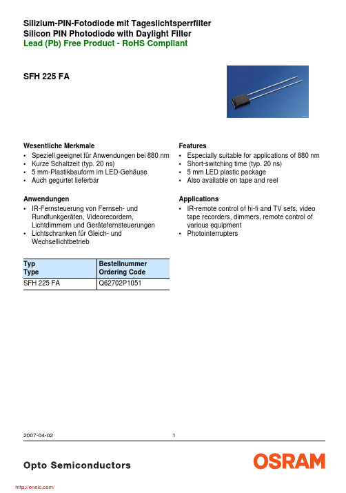
SFH 225 FASilizium-PIN-Fotodiode mit Tageslichtsperrfilter Silicon PIN Photodiode with Daylight FilterLead (Pb) Free Product - RoHS Compliant2007-04-021Wesentliche Merkmale •Speziell geeignet für Anwendungen bei 880 nm •Kurze Schaltzeit (typ. 20 ns)• 5 mm-Plastikbauform im LED-Gehäuse •Auch gegurtet lieferbarAnwendungen•IR-Fernsteuerung von Fernseh- und Rundfunkgeräten, Videorecordern,Lichtdimmern und Gerätefernsteuerungen •Lichtschranken für Gleich- und WechsellichtbetriebTyp Type Bestellnummer Ordering Code SFH 225 FAQ62702P1051Features •Especially suitable for applications of 880 nm •Short-switching time (typ. 20 ns)• 5 mm LED plastic package•Also available on tape and reelApplications•IR-remote control of hi-fi and TV sets, video tape recorders, dimmers, remote control of various equipment •PhotointerruptersGrenzwerte Maximum RatingsBezeichnung Parameter SymbolSymbolWertValueEinheitUnitBetriebs- und Lagertemperatur Operating and storage temperature range Top; T stg– 40 … + 100°CSperrspannung Reverse voltage VR20VVerlustleistung, T A = 25 °C Total power dissipation Ptot150mWKennwerte (T A = 25 °C, λ = 870 nm) CharacteristicsBezeichnung Parameter SymbolSymbolWertValueEinheitUnitFotostrom PhotocurrentV R = 5 V, E e = 1 mW/cm2IP34 (≥ 25)μAWellenlänge der max. FotoempfindlichkeitWavelength of max. sensitivityλS max900nmSpektraler Bereich der FotoempfindlichkeitS = 10 % von SmaxSpectral range of sensitivityS = 10 % of Smaxλ740 … 1120nmBestrahlungsempfindliche FlächeRadiant sensitive areaA 4.84mm2Abmessung der bestrahlungsempfindlichen Fläche Dimensions of radiant sensitive area L×BL×W2.20 × 2.20mm × mmHalbwinkel Half angle ϕ± 60Graddeg.Dunkelstrom, V R = 10 V Dark current IR2 (≤ 30)nASpektrale Fotoempfindlichkeit Spectral sensitivity Sλ0.63A/WQuantenausbeute Quantum yield η0.90ElectronsPhotonLeerlaufspannung, E e = 0.5 mW/cm2 Open-circuit voltage VO330 (≥ 250)mV2007-04-0222007-04-023Kurzschlußstrom, E e = 0.5 mW/cm 2 Short-circuit currentI SC 17μA Anstiegs- und Abfallzeit des Fotostromes Rise and fall time of the photocurrentR L = 50 Ω; V R = 5 V; λ = 850 nm; I p = 800 μA t r , t f20nsDurchlaßspannung, I F = 100 mA, E = 0 Forward voltageV F 1.3V Kapazität, V R = 0 V, f = 1 MHz, E = 0 CapacitanceC 048pF Temperaturkoeffizient von V O Temperature coefficient of V O TC V – 2.6mV/K Temperaturkoeffizient von I SC Temperature coefficient of I SCTC I 0.18%/K Rauschäquivalente Strahlungsleistung Noise equivalent power V R = 10 VNEP3.6 × 10– 14Nachweisgrenze, V R = 10 V Detection limitD*6.1 × 10¹²Kennwerte (T A = 25 °C, λ = 870 nm) Characteristics (cont’d)Bezeichnung ParameterSymbol SymbolWert Value Einheit Unit W Hz -----------cm Hz ×W--------------------------2007-04-024Relative Spectral SensitivityDark CurrentPhotocurrent I P = f (E e ), V R = 5 VCapacitanceTotal Power Dissipation Dark CurrentMaßzeichnungPackage OutlinesMaße in mm (inch) / Dimensions in mm (inch).LötbedingungenSoldering ConditionsWellenlöten (TTW)(nach CECC 00802)2007-04-025OSRAM Opto Semiconductors GmbHWernerwerkstrasse 2, D-93049 Regensburg© All Rights Reserved.The information describes the type of component and shall not be considered as assured characteristics.Terms of delivery and rights to change design reserved. Due to technical requirements components may contain dangerous substances. For information on the types in question please contact our Sales Organization.PackingPlease use the recycling operators known to you. We can also help you – get in touch with your nearest sales office. By agreement we will take packing material back, if it is sorted. You must bear the costs of transport. For packing material that is returned to us unsorted or which we are not obliged to accept, we shall have to invoice you for any costs incurred.Components used in life-support devices or systems must be expressly authorized for such purpose! Critical components 1 , may only be used in life-support devices or systems 2 with the express written approval of OSRAM OS.1 A critical component is a component usedin a life-support device or system whose failure can reasonably be expected to cause the failure of that life-support device or system, or to affect its safety or effectiveness of that device or system.2 Life support devices or systems are intended (a) to be implanted in the human body, or (b) to support and/or maintain and sustain human life. If they fail, it is reasonable to assume that the health of the user may be endangered.2007-04-026分销商库存信息: OSRAMSFH 225 FA。
BCB1012UH-F00;中文规格书,Datasheet资料

Descriptions:1. Delta will not guarantee the performance of the products if the application condition fallsoutside the parameters set forth in the specification.2. A written request should be submitted to Delta prior to approval if deviation from thisspecification is required.3. Please exercise caution when handling fans. Damage may be caused when pressure is appliedto the impeller, if the fans are handled by the lead wires, or if the fans are hard-dropped to the production floor.4. Except as pertains to some special designs, there is no guarantee that the products will be freefrom any such safety problems or failures as caused by the introduction of powder, droplets of water or encroachment of insect into the hub.5. The above-mentioned conditions are representative of some unique examples and viewed as thefirst point of reference prior to all other information.6. It is very important to establish the correct polarity before connecting the fan to the powersource. Positive (+) and Negative (-). Damage may be caused to the fans if connection is with reverse polarity, as there is no foolproof method to protect against such error.7. Delta fans are not suitable where any corrosive fluids are introduced to their environment.8. Please ensure all fans are stored according to the storage temperature limits specified. Do notstore fans in a high humidity environment. We highly recommend performance testing is conducted before shipping, if the fans have been stored over 6 months.9. Not all fans are provided with the Lock Rotor Protection feature. If you impair the rotation ofthe impeller for the fans that do not have this function, the performance of those fans will lead to failure.10. Please be cautious when mounting the fan. Incorrect mounting of fans may cause excessresonance, vibration and subsequent noise.11. It is important to consider safety when testing the fans. A suitable fan guard should be fitted tothe fan to guard against any potential for personal injury.12. Except where specifically stated, all tests are carried out at relative (ambient) temperature andhumidity conditions of 25o C, 65%. The test value is only for fan performance itself.13. Be certain to connect an “over 4.7µF” capacitor to the fan externally when the application callsfor using multiple fans in parallel, to avoid any unstable power.分销商库存信息: DELTA-PRODUCT-GROUPS BCB1012UH-F00。
IRMCK203;中文规格书,Datasheet资料
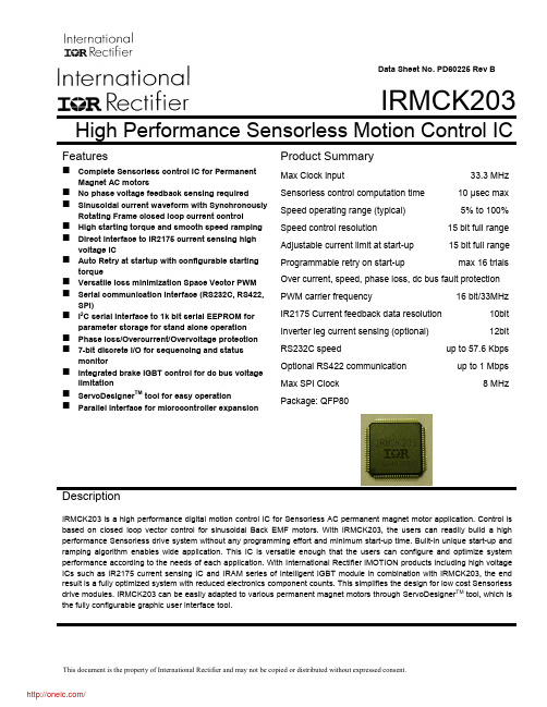
Data Sheet No. PD60225 Rev BIRMCK203High Performance Sensorless Motion Control ICFeaturesComplete Sensorless control IC for PermanentMagnet AC motorsNo phase voltage feedback sensing required Sinusoidal current waveform with SynchronouslyRotating Frame closed loop current control High starting torque and smooth speed ramping Direct interface to IR2175 current sensing highvoltage IC Auto Retry at startup with configurable startingtorque Versatile loss minimization Space Vector PWM Serial communication interface (RS232C, RS422,SPI) I 2C serial interface to 1k bit serial EEPROM forparameter storage for stand alone operation Phase loss/Overcurrent/Overvoltage protection 7-bit discrete I/O for sequencing and statusmonitorIntegrated brake IGBT control for dc bus voltage limitation ServoDesigner TM tool for easy operationParallel interface for microcontroller expansionProduct SummaryMax Clock input33.3 MHz Sensorless control computation time 10 µsec max Speed operating range (typical) 5% to 100% Speed control resolution15 bit full range Adjustable current limit at start-up 15 bit full range Programmable retry on start-upmax 16 trialsOver current, speed, phase loss, dc bus fault protection PWM carrier frequency16 bit/33MHzIR2175 Current feedback data resolution 10bit Inverter leg current sensing (optional) 12bitRS232C speedup to 57.6 Kbps Optional RS422 communication up to 1 MbpsMax SPI Clock 8 MHzPackage: QFP80DescriptionIRMCK203 is a high performance digital motion control IC for Sensorless AC permanent magnet motor application. Control is based on closed loop vector control for sinusoidal Back EMF motors. With IRMCK203, the users can readily build a high performance Sensorless drive system without any programming effort and minimum start-up time. Built-in unique start-up and ramping algorithm enables wide application. This IC is versatile enough that the users can configure and optimize system performance according to the needs of each application. With International Rectifier iMOTION products including high voltage ICs such as IR2175 current sensing IC and IRAM series of Intelligent IGBT module in combination with IRMCK203, the end result is a fully optimized system with reduced electronics component counts. This simplifies the design for low cost Sensorless drive modules. IRMCK203 can be easily adapted to various permanent magnet motors through ServoDesigner TM tool, which is the fully configurable graphic user interface tool.OverviewIRMCK203 is a new International Rectifier integrated circuit device designed for one-chip solution for complete closed loop current and velocity control of a high performance Sensorless drive for PM motors. Unlike a traditional microcontroller or DSP, IRMCK203 does not require any programming to complete complex Sensorless algorithm development. Combined with International Rectifier's high voltage gate drive and current sensing IC, the user can implement complete speed control of PM motors with minimum component count and virtually no design effort. In addition to Sensorless closed loop speed control operation, features such as Start-up retry, Phase Loss detection, Low Loss PWM, Regeneration Braking control and various drive protections are all implemented inside IRMCK203. Analog and digital I/Os can also be configured. Host communication logic contains Asynchronous Communication Interface for RS232C or RS422 communication interface, a fast slave SPI interface and an 8 bit wide Host Parallel Interface. All communication ports have the same access capability to the host register set. The users can write to, and read from the predefined registers to configure and monitor the drive through these communication ports.IRMCK203 Main functions• Complete closed loop current control based on Synchronously Rotating Frame Field Orientation (using Rotor Angle Observer)• Closed loop velocity control based on estimated speed• Configurable parameters (PI controller gains, PI output limit range, current feedbackscaling, PWM carrier frequency) provide adaptation to various PM motors• Built-in Sensorless control logic for start-up, ramping, and running conditions• Auto Retry (programmable) on start-up with configurable torque current limit• Analog reference input (can be used for speed reference)• RS232C/RS422 reference input• Full dynamic braking control for DC bus voltage limitation• Cycle-by-cycle on/off Control for Brake IGBT• Loss minimization Space Vector PWM with deadtime insertion• Build-in two IR2175 current sensing IC interfaces• Phase Loss, Overcurrent (GATEKILL input), Overvoltage, Undervoltage, Overspeed protection• Low cost serial 12bit A/D interface with multiplexer and sample/hold circuit• Optional Inverter Leg (low side) current sensing in lieu of IR2175 IC• 4 channel analog output (PWM)• Local EEPROM for startup initialization of internal data/parameters through host register interface AT24C01A, 128X8• Versatile host communication interfaceRS232C or RS422 host interfaceFast SPI slave host interface with multi-drop capabilityParallel Host interface (total 12 pins)• Multiplexed data/address busAddress EnableRD/WR• Discrete I/Os for Standalone mode operationSTARTSTOP (Input)ESTOP (Input)DIR (Input) FLTCLR (Input) FAULT (Output) SYNC (Output) REDLED (Output)GREENLED (Output)Table of Contents Overview (2)IRMCK203 Main functions (2)IRMCK203 Block Diagrams (7)Basic Block Diagram (7)Input/Output of IRMCK203 (8)Application Connections (12)IC Crystal Clock Circuitry (13)PLL Clock Circuitry (14)Low Pass Filter (14)Implementing the Low Pass Filter Shield (15)Cp Rp and Cs Component Values (15)PLL Reset (15)DC Electrical Characteristics and Operating Conditions (16)Absolute Maximum Ratings (16)Recommended Operating Conditions (16)DC Characteristics (17)Common Quiescent and Leakage Current (17)Input Characteristics – Non Schmitt Inputs (17)Input Characteristics – Schmitt Inputs (17)Output Characteristics (17)Output Characteristics OSC2CLK (18)Pin and I/O Characteristic Table (19)Power Consumption (21)AC Electrical Characteristics and Operating Conditions (22)System Level AC Characteristics (22)Sync Pulse to Sync Pulse Timing (22)FAULT and REDLED Response to GATEKILL (23)Host Interface AC Characteristics (24)SPI Timing (24)Host Parallel Timing (25)Host Parallel Read Cycle (25)Host Parallel Write Cycle (26)Discrete I/O Electrical Characteristics (27)Motion Peripheral Electrical Characteristics (28)PWM Electrical Characteristics (28)IR2175 Interface (28)Analog Interface Electrical Characteristics (29)ADC Timing (29)PLL Interface Electrical Characteristics (30)Appendix A Host Register Map (31)Register Access (31)Host Parallel Access (31)SPI Register Access (31)RS-232 Register Access (31)Write Register Definitions (36)PwmConfig Register Group (Write Registers) (36)CurrentFeedbackConfig Register Group (Write Registers) (37)SystemControl Register Group (Write Registers) (38)TorqueLoopConfig Register Group (Write Registers) (38)VelocityControl Register Group (Write Registers) (39)IRMCK203 FaultControl Register Group (Write Registers) (40)SystemConfig Register Group (Write Registers) (41)EepromControl Registers (Write Registers) (42)ClosedLoopAngleEstimator Registers (Write Registers) (43)OpenLoopAngleEstimator Registers (Write Registers) (44)StartupAngleEstimator Registers (Write Registers) (44)StartupRetrial Registers (Write Registers) (45)PhaseLossDetect Registers (Write Registers) (47)D/AConverter Registers (Write Registers) (47)Factory Test Register (Write Register) (48)Read Register Definitions (49)SystemStatus Register Group (Read Registers) (49)DcBusVoltage Register Group (Read Registers) (49)FocDiagnosticData Register Group (Read Registers) (50)FaultStatus Register Group (Read Registers) (51)VelocityStatus Register Group (Read Registers) (52)CurrentFeedbackOffset Register Group (Read Registers) (53)EepromStatus Registers (Read Registers) (53)FOCDiagnosticDataSupplement Register Group (Read Registers) (54)ProductIdentification Registers (Read Registers) (55)Factory Register (Read Register) (55)Appendix B Package (56)Table of FiguresFigure 1: IRMCS2031 Simplified Blocks (7)Figure 2: Input/Output of IRMCK203 (8)Figure 3: Application Connection of IRMCK203 (12)Figure 4: Oscillator Circuit (13)Figure 5: PLL Low Pass Filter Shielding (14)Figure 6: System Level SYNC To SYNC Timing (22)Figure 7: FAULT and REDLED Response to GATEKILL (23)Figure 8: SPI Timing (24)Figure 9: Host Parallel Read Cycle (25)Figure 10: Host Parallel Write Cycle (26)Figure 11: Discrete I/O Timing (27)Figure 12: PWM Timing (28)Figure 13: IR2175 Interface (28)Figure 14: Top Level ADC Timing (29)Table of TablesTable 1: Typical Values for the Clock Circuit (13)Table 2: PLL Test Pin Assignments (14)Table 3: PLL Low Pass Filter Values (15)Table 4: Absolute Maximum Ratings (16)Table 5: Recommended Operating Conditions (16)Table 6: DC Characteristics (17)Table 7: Non Schmitt Input Characteristics (17)Table 8: Schmitt Input Characteristics (17)Table 9: Output Characteristics (17)Table 10: Output Characteristics OSC2CLK (18)Table 11: Pin and I/O Characteristics (21)Table 12: IRMCK203 Power Consumption (21)Table 13: System Level SYNC to SYNC Timing (22)Table 14: FAULT and REDLED Response to GATEKILL (23)Table 15: SPI Timing (24)Table 16: Host Parallel Read Cycle Timing (25)Table 17: Host Parallel Write Cycle Timing (26)IRMCK203 Block DiagramsBasic Block DiagramFigure 1 shows the basic block diagram of the IRMCK203 surrounded by International Rectifiers’ ICs. Host communications are provided over SPI, RS-232C or Host parallel ports. Two current sensing ICs (IR2175) and a three phase high voltage gate drive typically implement the high voltage / current interface between the IRMCK203 IC and motor.The IRMCK203 can operate in a “stand-alone” mode without the host controller. A serial EEPROM would be utilized to load motor-specific parameters into the IC.AC PowerConfigurable parameters are provided to tailor design to various applications (motor and load). These configurable parameters can be modified via the host register interface through the communication interface. In the IRMCK203 product, a design spread sheet is provided to aid the user for ease of drive start-up, the spread sheet will input high level application data such as motor name plate information, max speed, current limit, speed and current regulator bandwidth, base on this information the program will generate the required configurable parameters. Detail on Drive commissioning is described in the IRMCK203 Application Developer’s Guide.All logic and algorithms are pre-programmed, and the user does not need to make any effort to develop code, alleviating the tedious design process. If needed, the user can configure the drive to tailor the control per specificneeds to meet the required specification. This configuration can be easily done by accessing the host register interface through the communication interface.Input/Output of IRMCK203The I/O signals are shown in Figure 2. The interface signals are divided into sub-groups. For detailed pin assignment, please refer to appendix (Pin definition).PWMUH PWMUL PWMVL BRAKEGATEKILLIFB[0-1]ADCLK ADOUT ADCONVST ADMUX[0-2]RESSAMPLEPWM gate signalInterfaceIR2175 Interface A/D InterfaceSPI Interface Parallel InterfaceLED/StatusPLL Clock ControlCrystalDAC[0-3]D/A Interface (PWM output)RESETNSystem ResetFLTCLROUT Figure 2: Input/Output of IRMCK203Host Interface GroupSignal Input (I) /Output (O)Low (L) /High (H) TrueAsserted FunctionSPICLK IPositive edgesensitiveSPI clockSPIMISO O - Master input and slave output SPIMOSI I - Master output and slave input SPICSN I L SPI chip selectHP_nOE I LParallel data output enable HP_nWE I LParallel data write cycleidentificationHP_D [7:0] I/O - Parallel dataHP_A I HParallel data address cycleidentificationHP_nCS I L Chip select TX O - RS-232 data out RX I - RS-232 data inBAUDSEL[1:0] I H RS-232 baud rate: 00 = 19.3K bps;01 = 38.4K bps10 = 57.6K bps;11 = 1.031250M bpsSYNC O L Start of PWM cycleCLK1XOUT O -33.333 MHz output of PLL. This signal has no phase relationshipwith the OSC1CLK or OSC2CLK inputs.Discrete I/O GroupSignalInput (I) / Output (O)Low (L) / High (H) True AssertedFunctionSTARTSTOP I HStart / Stop command edgesensitiveDIR I HForward/Reverse Directioncommand, level sensitiveFAULTCLR I H Fault ClearESTOP I HEmergency Stop, statesensitivePWEN O H PWM enable/disable state SYNC O H SYNC pulse FAULT O H Fault stateMotion Peripheral GroupSignalInput (I) / Output (O)Low (L) / High (H) True AssertedFunctionPWMUH O PWM phase U high side PWMUL O PWM phase U low side PWMVH O PWM phase V high sidePWHVL O PWM phase V low side PWMWH O PWM phase W high side PWMWL O -PWM phase W low side BRAKE O L IGBT gateGATEKILL I Varies, Based onWrite Register0x0C Bit 7When asserted, negates all sixPWM signals, host writeableIFB0 I - Channel 0 (phase V) IFB1 I - Channel 1 (phase W)Analog Interface GroupSignal Input (I) /Output (O)Low (L) /High (H) TrueAsserted FunctionADCLK ONegative EdgeSensitiveClock to ADS7818ADOUT I - Serial data from ADS7818 DAC [3:0] O - Diagnostic DACADCONVST O LConversion start to ADS7818 RESSAMPLE OSample/hold control signalchannel 0 A/D converterADMUX0 O H Analog input MUX select ADMUX1 O H Analog input MUX selectPLL Interface GroupSignal Input (I) /Output (O)Low (L) /High (H) True AssertedFunctionXPD I L PLL reset RESETN I L Digital logic resetBYPASSCLK I HInternal test pin – force to logiclowBYPASSMODE I HInternal test pin – force to logiclowOSC1CLK I - 33.33 MHz crystal input OSC2CLK I - 33.33 MHz crystal inputPLLTEST I HInternal test pin – force to logiclowCHGO I/O - Low pass filter LPVSS I/O - Low pass filter ground分销商库存信息: IRIRMCK203。
DS1603;中文规格书,Datasheet资料
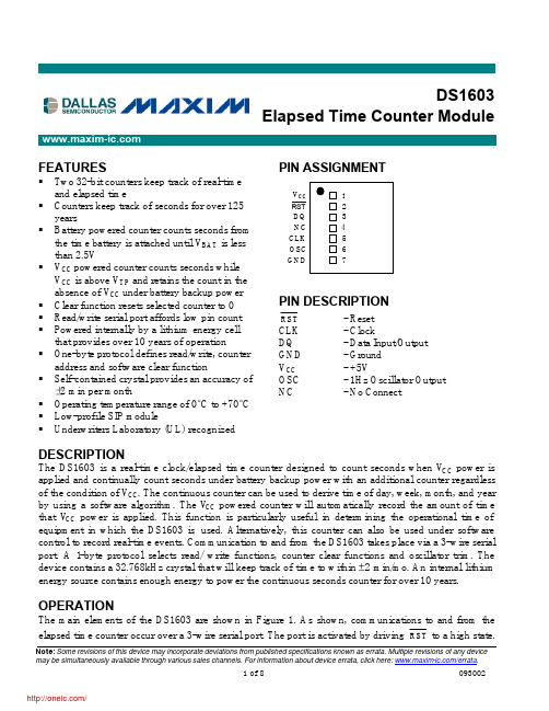
Note: Some revisions of this device may incorporate deviations from published specifications known as errata. Multiple revisions of any device may be simultaneously available through various sales channels. For information about device errata, click here: /errata .FEATURES§ Two 32-bit counters keep track of real -time and elapsed time§ Counters keep track of seconds for over 125 years§ Battery powered counter counts seconds from the time battery is attached until V BAT is less than 2.5V§ V CC powered counter counts seconds while V CC is above V TP and retains the count in the absence of V CC under battery backup power § Clear function resets selected counter to 0 § Read/write serial port affords low pin count § Powered internally by a lithium energy cell that provides over 10 years of operation§ One-byte protocol defines read/write, counter address and software clear function§ Self-contained crystal provides an accuracy of ±2 min per month§ Operating temperature range of 0°C to +70°C § Low-profile SIP module§ Underwriters Laboratory (UL) recognized PIN ASSIGNMENTPIN DESCRIPTIONRST- Reset CLK - ClockDQ - Data Input/Output GND - Ground V CC - +5VOSC - 1Hz Oscillator Output NC- No ConnectDESCRIPTIONThe DS1603 is a real -time clock/elapsed time counter designed to count seconds when V CC power is applied and continually count seconds under battery backup power with an additional counter regardless of the condition of V CC . The continuous counter can be used to derive time of day, week, month, and year by using a software algorithm. The V CC powered counter will automatically record the amount of time that V CC power is applied. This function is particularly useful in determining the operational time of equipment in which the DS1603 is used. Alternatively, this counter can also be used under software control to record real -time events. Communication to and from the DS1603 takes place via a 3-wire serial port. A 1-byte protocol selects read/ write functions, counter clear functions and oscillator trim. The device contains a 32.768kHz crystal that will keep track of time to within ±2 min/mo. An internal lithium energy source contains enough energy to power the continuous seconds counter for over 10 years.OPERATIONThe main elements of the DS1603 are shown in Figure 1. As shown, communications to and from the elapsed time counter occur over a 3-wire serial port. The port is activated by driving RST to a high state.V CC RST DQ NC CLK OSC GND DS1603Elapsed Time Counter Moduleselect, register clear, and oscillator trim information. Each bit is serially input on the rising edge of the clock input. After the first eight clock cycles have loaded the protocol register with a valid protocol additional clocks will output data for a read or input data for a w rite. V CC must be present to access the DS1603. If V CC < V TP, the DS1603 will switch to internal power and disable the serial port to conserve energy. When running off of the internal power supply, only the continuous counter will continue to count and the counter powered by V CC will stop, but retain the count, which had accumulated when V CC power was lost. The 32-bit V CC counter is gated by V CC and the internal 1Hz signal.PROTOCOL REGISTERThe protocol bit definition is shown in Figure 2. Valid protocols and the resulting actions are shown in Table 1. Each data transfer to the protocol register designates what action is to occur. As defined, the MSB (bit 7 which is designated ACC) selects the 32-bit continuous counter for access. If ACC is a logical 1 the continuous counter is selected and the 32 clock cycles that follow the protocol will either read or write this counter. If the counter is being read, the contents will be latched into a different register at the end of protocol and the latched contents will be read out on the next 32 clock cycles. This avoids reading garbled data if the counter is clocked by the oscillator during a read. Similarly, if the counter is to be written, the data is buffered in a register and all 32 bits are jammed into the counter simultaneously on the rising edge of the 32nd clock. The next bit (bit 6 which is designated AVC) selects the 32–bit V CC active counter for access. If AVC is a logical 1 this counter is selected and the 32 clock cycles that follow will either read or write this counter. If both bit 7 and bit 6 are written to a logic high, all clock cycles beyond the protocol are ignored and bit 5, 4, and 3 are loaded into the oscillator trim register. A value of binary 3 (011) will give a clock accuracy of ±120 seconds per month at +25°C. Increasing the binary number towards 7 will cause the real-time clock to run faster. Conversely, lowering the binary number towards 0 will cause the clock to run slower. Binary 000 will stop the oscillator completely. This feature can be used to conserve battery life during storage. In this mode the internal power supply current is reduced to 100 nA maximum. In applications where oscillator trimming is not practical or not needed, a default setting of 011 is recommended. Bit 2 of protocol (designated CCC) is used to clear the continuous counter. When set to logic 1, the continuous counter will reset to 0 when RST is taken low. Bit 1 of protocol (designated CVC) is used to clear the V CC active counter. When set to logical 1, the V CC active counter will reset to 0 when RST is taken low. Both counters can be reset simultaneously by setting CCC and CVC both to a logical 1. Bit 0 of the protocol (designated RD) determines whether the 32 clocks to follow w ill write a counter or read a counter. When RD is set to a logical 0 a write action will follow when RD is set to a logical 1 a read action will follow. When sending the protocol, 8 bits should always be sent. Sending less than 8 bits can produce erroneous results. If clearing the counters or trimming the oscillator, the data transfer can be terminated after the 8-bit protocol is sent. However, when reading or writing the counters, 32 clock cycles should always follow the protocol.RESET AND CLOCK CONTROLAll data transfers are initiated by driving the RST input high. The RST input has two functions. First, RST turns on the serial port logic, which allows access to the protocol register for the protocol data entry. Second, the RST signal provides a method of terminating the protocol transfer or the 32-bit counter transfer. A clock cycle is a sequence of a rising edge followed by a falling edge. For write inputs, data must be valid during the rising edge of the clock. Data bits are output on the falling edge of the clock when data is being read. All data transfers terminate if the RST input is transitioned low and the DQ pin goes to a high-impedance state. RST should only be transitioned low while the clock is high to avoid disturbing the last bit of data. All data transfers must consist of 8 bits when transferring protocol only or 8 + 32 bits when reading or writing either counter. Data tran sfer is illustrated in Figure 3.DATA INPUTFollowing the 8-bit protocol that inputs write mode, 32 bits of data are written to the selected counter on the rising edge of the next 32 CLK cycles. After 32 bits have been entered any additional CLK cycles will be ignored until RST is transitioned low to end data transfer and then high again to begin new data transfer.DATA OUTPUTFollowing the eight CLK cycles that input read mode protocol, 32 bits of data will be output from the selected counter on the next 32 CLK cycles. The first data bit to be transmitted from the selected 32-bit counter occurs on the falling edge after the last bit of protocol is written. When transmitting data from the selected 32-bit counter, RST must remain at high level as a transition to low level will terminate data transfer. Data is driven out the DQ pin as long as CLK is low. When CLK is high the DQ pin is tristated. OSCILLATOR OUTPUTPin 6 of the DS1603 module is a 1Hz output signal. This signal is present only when V CC is applied and greater than the internal power supply. However, the output is guaranteed to meet TTL requirement only while V CC is within normal limits. This output can be used as a 1-second interrupt or time tick needed in some applications.INTERNAL POWERThe internal battery of the DS1603 module provides 35mAh and will run the elapsed time counter for over 10 years in the absence of power.PIN DESCRIPTIONSV CC, GND – DC power is provided to the device on these pins. V CC is the +5V input. When 5V is applied within normal limits, the device is fully accessible and data can be written and read. When a 3V battery is connected to the device and V CC is below 1.25 x V BAT, reads and writes are inhibited. As V CC falls below V BAT the continuous counter is switched over to the internal battery.CLK (Serial Clock Input) – CLK is used to synchronize data movement on the serial interface.DQ (Data Input/Output) – The DQ pin is the bi-directional data pin for the 3-wire interface.RST (Reset) – The reset signal must be asserted high during a read or a write.OSC (One Hertz Output Signal) – This signal is only present when Vcc is at a valid level and the oscillator is enabled.Figure 1. ELAPSED TIME COUNTER BLOCK DIAGRAMFigure 2. PROTOCOL BIT MAP7 6 5 4 3 2 1 0ACC AVC OSC2 OSC1 OSC0 CCC CVC RDTable 1. VALID PROTOCOLSPROTOCOLACTIONACC AVC OSC2 OSC1 OSC0 CCC CVC RDFUNCTION ReadContinuous Counter 1 0 X X X X X 1Output continuouscounter on the 32 clocksfollowing protocol.Oscillator trim registeris not updated. Countersare not reset.WriteContinuous Counter 1 0 X X X X X 0Input data to continuouscounter on the 32 clocksfollowing protocol.Oscillator trim registeris not updated. Countersare not reset.Read V CCActive Counter 0 1 X X X X X 1Output V CC activecounter on the 32 clocksfollowing protocol,oscillator trim registeris not updated. Countersare not reset.Write V CCActive Counter 0 1 X X X X X 0Input data to continuouscounter on the 32 clocksfollowing protocol.Oscillator trim registeris not updated. Countersare not reset.ClearContinuous Counter 0 0 X X X 1 X XResets the continuouscounter to all zeros atthe end of protocol.Oscillator trim registeris not updated.Clear V CCActive Counter 0 0 X X X X 1 XResets the V CC activecounter to all zeros atthe end of protocol.Oscillator trim registeris not updated.Set Oscillator Trim Bits 1 1 A B C X X 0Sets the oscillator trimregister to a value ofABC. Counters areunaffected.X = Don’t CareFigure 3. DATA TRANSFERTIMING DIAGRAM: READ/WRITE DATA TRANSFERNote: t CL, t CH, t R, and t F apply to both read and write data transfer.ABSOLUTE MAXIMUM RATINGSVoltage Range on Any Pin Relative to Ground -0.3V to +7.0VOperating Temperature Range 0°C to +70°CStorage Temperature Range -40°C to +70°CSoldering Temperature Range See IPC/JEDEC J-STD-020A (See Note 11)This is a stress rating only and functional operation of the device at these or any other conditions beyond t h ose indicated in the operation sections of this specification is not implied. Exposure to absolute maximum rating conditions for extended periods of time can affect reliability.RECOMMENDED DC OPERATING CONDITIONS (0°C to +70°C) PARAMETER SYMBOL MIN TYP MAX UNITS NOTES Supply Voltage V CC 4.5 5.0 5.5 V 1 Logic 1 Input V IH 2.0 V CC + 0.3 V 1 Logic 0 Input V IL-0.3 0.8 V 1DC ELECTRICAL CHARACTERISTICS (0°C to +70°C; V CC = 5V ±10%) PARAMETER SYMBOL MIN TYP MAX UNITS NOTES Input Leakage I LI-1 +1 µAI/O Leakage I LO-1 +1 µALogic 1 Output V OH 2.4 V 2 Logic 0 Output V OL0.4 V 3 Active Supply Current I CC 1 mA 4 Timekeeping Current I CC150 µA 5 Battery Trip Point V TP 3.0 4.5 V 9 CAPACITANCE (T A = +25°C) PARAMETER SYMBOL MIN TYP MAX UNITS NOTES Input Capacitance C I 5 pFI/O Capacitance C I/O10 pF(T A = +25°C) PARAMETER SYMBOL MIN TYP MAX UNITS NOTES Expected Datat DR10 years 10 Retention TimeNOTES:1) All voltages are referenced to ground.2) Logic 1 voltages are specified at a source current of 1mA.3) Logic 0 voltages are specified at a sink current of 4mA.4) I CC is specified with the DQ pin open.5) I CC1 is specified with V CC at 5.0V and RST = GND.6) Measured at V IH= 2.0V or V IL = 0.8V.7) Measured at V OH = 2.4V or V OL - 0.4V.8) Load capacitance = 50pF.9) Battery trip point is the point at which the V CC powered counter and the serial port stops operation.The battery trip point drops below the minimum once the internal lithium energy cell is exhausted. 10) The expected t D R is defined as accumulative time in the absence of V CC with the clock oscillatorrunning.11) Real-time clock modules can be successfully processed through conventional wave-solderingtechniques as long as temperature exposure to the lithium energy source contained within does not exceed +85°C. Post-solder cleaning with water-washing techniques is acceptable, provided that ultrasonic vibration is not used.DS1603DS1603 7-PIN MODULEPKG7-PIN DIM MIN MAX A IN. MM 0.830 21.08 0.850 21.59 B IN. MM 0.650 16.51 0.670 17.02 C IN. MM 0.310 7.87 0.330 8.38 D IN. MM 0.015 0.38 0.030 0.76 E IN. MM 0.110 2.79 0.140 3.56 F IN. MM 0.015 0.38 0.021 0.53 G IN. MM 0.090 2.29 0.110 2.79 H IN. MM 0.105 2.67 0.135 3.43 J IN. MM 0.360 9.14 0.390 9.91分销商库存信息: MAXIMDS1603。
FFB0412VHN-R00;FFB0412VHN-F00;中文规格书,Datasheet资料

1.2
30
FFB0412/24XN
1.0
25
0.8
20
Air Pressure
0.6 15
0.4 10
0.2
5
0
0Leabharlann 0 0.15 0.3 0.45 0.6 0.75 (M3/MIN)
0
6 12 18 24
(CFM)
Air Flow
38.0 (1.496) 32.0 (1.260)
38.0 (1.496) 32.0 (1.260)
* Weight : 47g (1.66 oz)
Air Pressure
10.0 (0.394) 338.0±10.0
(13.310±0.394)
8-Ø3.5±0.3 (8-Ø0.138±0.012)
UNIT : mm (INCH)
■ P & Q CURVE (AT RATED VOLTAGE) ■ MOUNTING PANEL CUTOUT
mm UNIT: (INCH)
MODEL
Rated Voltage
PART NO. FFB0412MN FFB0424MN FFB0412HN FFB0424HN FFB0412HHN FFB0424HHN FFB0412VHN FFB0424VHN FFB0412SHN
FUNCTION -R00/-F00 -R00/-F00 -R00/-F00 -R00/-F00 -R00/-F00 -R00/-F00 -R00/-F00 -R00/-F00 -R00/-F00
(IN H2O) (mm H2O)
MODEL
Rated Voltage
PART NO. FFB0412VHN FFB0412SHN
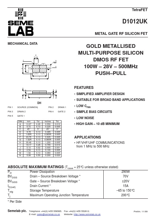
D1012UK中文资料
290W 70V ±20V 15A –65 to 150°C 200°C
元器件交易网
D1012UK
ELECTRICAL CHARACTERISTICS (Tcase = 25°C unless otherwise stated) Parameter Test Conditions Min.
THERMAL DATA
RTHj–case Thermal Resistance Junction – Case Max. 0.6°C / W
Semelab plc.
Telephone +44(0)1455 556565. Fax +44(0)1455 552612. Website: E-mail: sales@
1 4 1 3 1 2 1 1 1 0
G a in d B
1 2 0 1 0 0
P o u t W
8 0 6 0 4 0 2 0 0 0 2 4 6
P in W
V d s = 2 8 V 2 4 6 P in W 8 1 0 1 2 P o u t D r a in E ffic ie n c y 1 4
Prelim. 11/99
元器件交易网
D1012UK
1 4 0
1 4 0 1 2 0 1 0 0 P o u t W 8 0 6 0 4 0 2 0 0 0 f = 5 0 0 M H z I d q = 1 .2 A 1 0 0 7 0 6 0 5 0 4 0 3 0 2 0 % D r a in E ffic ie n c y
• LOW Crss • SIMPLE BIAS CIRCUITS • LOW NOISE • HIGH GAIN – 10 dB MINIMUM
MISM-3V1B 10-15;中文规格书,Datasheet资料

ELECTRICAL RATINGS
Contact Form A - Normally Open
Contact Rating (1) Voltage Current Resistance Capacitance
Power Switching Breakdown Switching Carry Contact, Initial Insulation Contact
(.059
+.004 -0
)
1,50
+0,10 -0
REEL DIMENSIONS (in) mm
(.059 +.-0004) Ø1,50 +0,10
-0
(.069) 1,75
3.0° (.559) 14,20
(1.118) 28,40
(1.260) 32,00
(.079) Ø2,00
(.050) 1,27
(1.276+-0.008) (32,4+-00.2 ) MEASURED AT HUB
120° TYP.
Hamlin USA
Tel: +1 920 648 3000 Fax: +1 920 648 3001 Email: @ DETAILS ON THIS DATA SHEET ARE PROVIDED FOR INFORMATION PURPOSES ONLY &
MISM-3V1 REED SWITCH
Features • Surface mounting normally open switch • Ultra-miniature size with 7.00mm x 1.80
mm (0.276” x 0.071”) glass envelope
- 1、下载文档前请自行甄别文档内容的完整性,平台不提供额外的编辑、内容补充、找答案等附加服务。
- 2、"仅部分预览"的文档,不可在线预览部分如存在完整性等问题,可反馈申请退款(可完整预览的文档不适用该条件!)。
- 3、如文档侵犯您的权益,请联系客服反馈,我们会尽快为您处理(人工客服工作时间:9:00-18:30)。
Descriptions:
1. Delta will not guarantee the performance of the products if the application condition falls
outside the parameters set forth in the specification.
2. A written request should be submitted to Delta prior to approval if deviation from this
specification is required.
3. Please exercise caution when handling fans. Damage may be caused when pressure is applied
to the impeller, if the fans are handled by the lead wires, or if the fans are hard-dropped to the production floor.
4. Except as pertains to some special designs, there is no guarantee that the products will be free
from any such safety problems or failures as caused by the introduction of powder, droplets of water or encroachment of insect into the hub.
5. The above-mentioned conditions are representative of some unique examples and viewed as the
first point of reference prior to all other information.
6. It is very important to establish the correct polarity before connecting the fan to the power
source. Positive (+) and Negative (-). Damage may be caused to the fans if connection is with reverse polarity, as there is no foolproof method to protect against such error.
7. Delta fans are not suitable where any corrosive fluids are introduced to their environment.
8. Please ensure all fans are stored according to the storage temperature limits specified. Do not
store fans in a high humidity environment. We highly recommend performance testing is conducted before shipping, if the fans have been stored over 6 months.
9. Not all fans are provided with the Lock Rotor Protection feature. If you impair the rotation of
the impeller for the fans that do not have this function, the performance of those fans will lead to failure.
10. Please be cautious when mounting the fan. Incorrect mounting of fans may cause excess
resonance, vibration and subsequent noise.
11. It is important to consider safety when testing the fans. A suitable fan guard should be fitted to
the fan to guard against any potential for personal injury.
12. Except where specifically stated, all tests are carried out at relative (ambient) temperature and
humidity conditions of 25o C, 65%. The test value is only for fan performance itself.
13. Be certain to connect an “over 4.7µF” capacitor to the fan externally when the application calls
for using multiple fans in parallel, to avoid any unstable power.
分销商库存信息: DELTA-PRODUCT-GROUPS BCB1012UH-F00。