RAMCloud Slides (Oct)
RAMCloud Slides

Offline
October 2, 2012 RAMCloud Slide 8
...
...
...
...
...
Goal: Scale and Latency
Traditional Application
Application Servers
Web Application
Storage Servers
RAMCloud
Research Issues
● Durability and availability ● Fast communication (RPC) ● Data model ● Concurrency, consistency, transactions ● Data distribution, scaling ● Multi-tenancy ● Client-server functional distribution ● Node architecture
Main-memory databases
UNIX buffer cache
Large file caches
Main-memory DBs, again
1970
October 2, 2012
1980
1990
RAMCloud
2000
2010
Slide 3
RAMCloud
Harness full performance potential of large-scale DRAM storage:
Hash Table Buffered Segment Disk
Backup
Buffered Segment Disk
Backup
莫贾UC-8580系列双核ARM Cortex-A7高速训练到地面计算机说明书

UC-8580SeriesArm Cortex-A7dual-core1GHz train-to-ground computers with4Mini PCIe expansion slots for wireless modulesFeatures and Benefits•Complies with all EN50155mandatory test items1•Supports up to3WWAN connections and2SIM card slots per cellularmodule•Supports1WLAN(IEEE802.11a/b/g/n/ac)connection•Single-panel I/O design for reduced installation space and easiermaintenance•Front-side access panel for easy maintenance•Isolated24to110VDC power input with power-ignition function suitable forvehicle applications•EN50155Tx(-40to70°C)operating temperature for harsh environments•5-year warrantyCertificationsIntroductionMoxa’s UC-8580is an innovative computing platform designed specifically for transportation applications.The UC-8580is available with one of two different types of antenna connectors.The SMA model supports all SMA type connectors.The QMA model supports TNC connectors for GPS and QMA connectors for Wi-Fi/cellular modules,and has four slots for installing wireless modules.2Three slots support4G LTE modules,and one slot supports a Wi-Fi module.Each4G LTE module has two SIM card slots,which can be used to enable redundant cellular network communications or geo-fencing SIM card selection by leveraging the built-in Wireless Manager,a Moxa software utility for cellular and Wi-Fi management.The UC-8580uses an open platform based on Debian8with Linux kernel4.1,allowing solution providers to manage software packages via Debian’s APT(Advanced Packaging Tools),or develop software applications with Moxa’s API Library and GNU C Library.The UC-8580’s single-sided I/O design is ideal for vehicle applications,which typically do not have a lot of room for installing communications devices.The UC-8580also has an access panel on the front side,allowing users to install or change wireless modules,SIM cards,or mSATA cards without removing the entire unit from the wall after being mounted.The UC-8580can be used as a communication-centric computing platform for the following applications:•Vehicle-to-ground communication gateway•TCMS T2G(train-to-ground)gateway•Mobile condition monitoring unit•Ethernet Consist Network T2G gateway•Onboard wireless automated fare collection unit1.This product is suitable for rolling stock railway applications,as defined by the EN50155standard.For a more detailed statement,click here:/doc/specs/EN_50155_Compliance.pdf2.Wireless modules are sold separately.Please contact a Moxa sales representative for details.AppearanceSMA ModelQMA ModelSpecificationsComputerCPU Armv7Cortex-A7dual-core1GHz System Memory Pre-installed1GB DDR3LSupported OS Linux Debian8(Linux kernel v4.1)Storage Slot mSATA slots x1,internal mini-PCIe socketStorage Pre-installed8GB eMMCComputer InterfaceEthernet Ports Auto-sensing10/100/1000Mbps ports(M12X-coded)x2 Serial Ports RS-232/422/485ports x2,software-selectable(terminal block) USB3.0USB3.0hosts x1,type-A connectorsDigital Input DIs x3Digital Output DOs x3Expansion Slots mPCIe slots x4Wi-Fi Antenna Connector UC-8580-LX/8580-T-LX/8580-T-CT-LX:RP-SMA x3UC-8580-Q-LX/8580-T-Q-LX/8580-T-CT-Q-LX:QMA x3 Cellular Antenna Connector UC-8580-LX/8580-T-LX/8580-T-CT-LX:SMA x6UC-8580-Q-LX/8580-T-Q-LX/8580-T-CT-Q-LX:QMA x6 Number of SIMs6SIM Format MiniGPS Antenna Connector UC-8580-LX/8580-T-LX/8580-T-CT-LX:SMA x1UC-8580-Q-LX/8580-T-Q-LX/8580-T-CT-Q-LX:TNC x1 Console Port RS-232(TxD,RxD,GND),4-pin header output(115200,n,8,1) Input/Output InterfaceButtons Reset buttonDigital InputsChannel-to-Channel Isolation3K VDCConnector Screw-fastened Euroblock terminalCounter Frequency25HzDry Contact On:short to GNDOff:openI/O Mode DIPoints per COM3x channelSensor Type Wet contact(NPN or PNP)Wet Contact(DI to COM)On:10to30VDCOff:0to3VDCDigital OutputsConnector Screw-fastened Euroblock terminalCurrent Rating200mA per channelI/O Type SinkVoltage0to30VDCLED IndicatorsSystem Power x1System Ready x1Programmable x1Wireless Signal Strength Cellular/Wi-Fi x12LAN2per port(10/100/1000Mbps)Serial2per port(Tx,Rx)Serial SignalsRS-232TxD,RxD,RTS,CTS,DTR,DSR,DCD,GNDRS-422Tx+,Tx-,Rx+,Rx-,GNDRS-485-2w Data+,Data-,GNDRS-485-4w Tx+,Tx-,Rx+,Rx-,GNDGPS InterfaceHeading Accuracy0.3degreesIndustrial Protocols NMEA0183,version4.0(V2.3or V4.1configurable),UBX,RTCM Receiver Types72-channel u-blox M8engineTime Pulse0.25Hz to10MHzVelocity Accuracy0.05msPower ParametersInput Current 1.66A@24VDC,0.36A@110VDCInput Voltage24to110VDCPower Connector M12A-coded4-pin male connectorPower Consumption40W(max.)Physical CharacteristicsHousing MetalIP Rating IP40Dimensions(with ears)270x134x88mm(10.63x5.28x3.46in)Dimensions(without ears)220x134x88mm(8.66x5.28x3.46in)Weight Product only:2,200g(4.85lb)Installation Wall mountingProtection-CT models:PCB conformal coatingEnvironmental LimitsOperating Temperature Standard Models:-25to55°C(-13to131°F)Wide Temp.Models:-40to70°C(-40to158°F)Storage Temperature(package included)-40to85°C(-40to185°F)Ambient Relative Humidity5to95%(non-condensing)Standards and CertificationsEMC EN55032/24EMI CISPR32,FCC Part15B Class AEMS IEC61000-4-2ESD:Contact:6kV;Air:8kVIEC61000-4-3RS:80MHz to1GHz:20V/mIEC61000-4-4EFT:Power:2kV;Signal:2kVIEC61000-4-5Surge:Power:2kV;Signal:2kVIEC61000-4-6CS:10VIEC61000-4-8PFMFRailway EN50121-4EN50155Railway Fire Protection EN45545-2Safety EN60950-1UL60950-1Shock IEC60068-2-27,IEC61373,EN50155:2017 Vibration IEC60068-2-64,IEC61373,EN50155:2017 DeclarationGreen Product RoHS,CRoHS,WEEEWarrantyWarranty Period5yearsDetails See /warrantyPackage ContentsDevice1x UC-8580Series computerCable1x4-pin header to DB9console cable Documentation1x quick installation guide1x warranty cardDimensionsOrdering InformationModel Name CPU Antenna Connector Type Operating Temp.Conformal CoatingUC-8580-LX Armv7Cortex-A7dual-core1GHzSMA-25to55°C–UC-8580-T-LX Armv7Cortex-A7dual-core1GHzSMA-40to70°C–UC-8580-T-CT-LX Armv7Cortex-A7dual-core1GHzSMA-40to70°C✓UC-8580-Q-LX Armv7Cortex-A7dual-core1GHzQMA-25to55°C–UC-8580-T-Q-LX Armv7Cortex-A7dual-core1GHzQMA-40to70°C–UC-8580-T-CT-Q-LX Armv7Cortex-A7dual-core1GHzQMA-40to70°C✓Accessories(sold separately)Wi-Fi Wireless ModulesUC-8580-WLAN33-AC3transmitter3receiver Wi-Fi card module,3SMA connectors with cablesUC-8500-WLAN33-Q-AC3transmitter3receiver Wi-Fi card module,3QMA connectors with cablesCellular Wireless ModulesUC-8500-4GCat6-Q-APAC LTE Cat.6module for North America and Europe,2QMA connectors with cables,-40to60°Coperating temperatureUC-8500-4GCat6-Q-NAMEU LTE Cat.6module for North America and Europe,2QMA connectors with cables,-40to60°Coperating temperatureUC-8580-4GCat6-NAMEU LTE Cat.6module for North America and Europe,2SMA connectors with cables,-40to60°Coperating temperaturePower AdaptersPWR-24250-DT-S1Power adapter,90to264VAC,24VDC,2.5A DC loadPower CordsPWC-C13US-3B-183Power cord with United States(US)plug,1.83mPWC-C13CN-3B-183Power cord with three-prong China(CN)plug,1.83mPWC-C13AU-3B-183Power cord with Australian(AU)plug,1.83mPWC-C13EU-3B-183Power cord with Continental Europe(EU)plug,1.83mPWC-C13JP-3B-183Power cord with Japan(JP)plug,7A/125V,1.83mPWC-C13UK-3B-183Power cord with United Kingdom(UK)plug,1.83m©Moxa Inc.All rights reserved.Updated Nov23,2022.This document and any portion thereof may not be reproduced or used in any manner whatsoever without the express written permission of Moxa Inc.Product specifications subject to change without notice.Visit our website for the most up-to-date product information.。
6130 磁盘阵列控制器托盘和 6130 磁盘阵列扩展托盘安装指南说明书
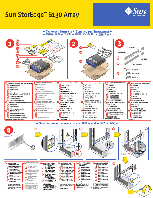
Part Number 819-2500-10Revision A of April 2005Sun Microsystems, Inc. © Copyright 2005 Sun Microsystems, Inc. All rights reserved. Use is subject to license terms. Third-party software, including font technology, is copyrighted and licensed from Sun suppliers. Portions may be derived from Berkeley BSD systems, licensed from U. of CA. Sun, Sun Microsystems, Sun StorEdge, the Sun logo, and Solaris are trademarks or registered trademarks of Sun Microsystems, Inc. in the U.S. and in other countries. All SP ARC trademarks are used under license and are trademarks or registered trademarks of SP ARC International, Inc. in the U.S. and in other countries. U.S. Government Rights–Commercial use. Government users are subject to the Sun Microsystems, Inc. standard license agreement and applicable provisions of the FAR and its supplements.© Copyright 2005 Sun Microsystems, Inc. Tous droits réservés. Distribué par des licences qui en restreignent l'utilisation. Le logiciel détenu par des tiers, et qui comprend la technologie relative aux polices de caractères, est protégé par un copyright et licencié par des fournisseurs de Sun. Des parties de ce produit pourront être dérivées des systèmes Berkeley BSD licenciés par l'Université de Californie. Sun, Sun Microsystems, Sun StorEdge, le logo Sun, et Solaris sont des marques de fabrique ou des marques déposées de Sun Microsystems, Inc. aux États-Unis et dans d'autres pays. Toutes les marques SP ARC sont utilisées sous licence et sont des marques de fabrique ou des marques déposées de SP ARC International, Inc. aux États-Unis et dans d'autres pays.。
Arduino Nano ESP32 产品参考手册说明书

Product Reference ManualSKU: ABX00083DescriptionThe Arduino Nano ESP32 (with and without headers) is a Nano form factor board based on the ESP32-S3 (embedded in the NORA-W106-10B from u-blox®). This is the first Arduino board to be based fully on an ESP32, and features Wi-Fi®, Bluetooth® LE, debugging via native USB in the Arduino IDE as well as low power.The Nano ESP32 is compatible with the Arduino IoT Cloud, and has support for MicroPython. It is an ideal board for getting started with IoT development.Target areas:Maker, Debugging, IoT, MicroPythonFeaturesXtensa® Dual-core 32-bit LX7 Microprocessor Up to 240 MHz384 kB ROM512 kB SRAM16 kB SRAM in RTC (low power mode)DMA ControllerPowerOperating voltage 3.3 VVUSB supplies 5 V via USB-C® connectorVIN range is 6-21 VConnectivityWi-Fi®Bluetooth® LEBuilt-in antenna2.4 GHz transmitter/receiverUp to 150 MbpsPins14x digital (21x including analog)8x analog (available in RTC mode)SPI(D11,D12,D13), I2C (A4/A5), UART(D0/D1) Communication PortsSPII2CI2SUARTCAN (TWAI®)Low Power7 μA consumption in deep sleep mode240 μA consumption in light sleep modeRTC MemoryUltra Low Power (ULP) CoprocessorPower Management Unit (PMU)ADC in RTC mode55556778888999910101011111111121212131313131314151516Contents1 The Board1.1 Application Examples 2 ESP32 Core3 Recommended Operating Conditions4 Block Diagram5 Board Topology5.1 Front View6 NORA-W106-10B (Radio Module / MCU)6.1 Xtensa® Dual-Core 32bit LX7 Microprocessor 6.2 Wi-Fi®6.3 Bluetooth®7 System7.1 Resets 7.2 Timers 7.3 Interrupts8 Serial Communication Protocols8.1 Inter-Integrated Circuit (I2C)8.2 Inter-IC Sound (I2S)8.3 Serial Peripheral Interface (SPI)8.4 Universal Asynchronous Receiver/Transmitter (UART)8.5 Two Wire Automotive Interface (TWAI®)9 External Flash Memory 10 USB Connector 11 Power Options11.1 Power Tree 11.2 Pin Voltage 11.3 VIN Rating 11.4 VUSB11.5 Using the 3.3 V Pin 11.6 Pin Current 12 Pinout12.1 Analog (JP1)12.2 Digital (JP2)13 Mounting Holes And Board Outline161617171717174191920202014 Board Operation14.1 Getting Started - IDE14.2 Getting Started - Arduino Web Editor 14.3 Getting Started - Arduino IoT Cloud 14.4 Online Resources 14.5 Board Recovery15 Declaration of Conformity CE DoC (EU)16 Declaration of Conformity to EU RoHS & REACH 211 01/19/202117 Conflict Minerals Declaration 18 FCC Caution19 Company Information 20 Reference Documentation 21 Change Log1 The BoardNano ESP32 is a 3.3 V development board based on the NORA-W106-10B from u-blox®, a module that includes a ESP32-S3 system on a chip (SoC). This module has support for Wi-Fi® and Bluetooth® Low Energy (LE), with amplified communication through a built-in antenna. The CPU (32-bit Xtensa® LX7) support clock frequencies at up to 240 MHz and has native support for debugging via the USB-C® connector.1.1 Application ExamplesHome automation: an ideal board for automating your home, and can be used for smart switches, automatic lighting and motor control for e.g. motor controlled blinds.IoT sensors: with several dedicated ADC channels, accessible I2C/SPI buses and a robust ESP32-S3 based radio module, this board can easily be deployed to monitor sensor values.Low power designs: create battery powered applications with low power consumption, utilising the built in low power modes of the ESP32-S3 SoC.2 ESP32 CoreThe Nano ESP32 uses the Arduino Core for ESP32 boards, a derivation of Espressif's arduino-esp32 core. Rating3 Recommended Operating ConditionsSymbol Description Min Typ Max UnitV IN Input voltage from VIN pad67.021VV USB Input voltage from USB connector 4.8 5.0 5.5VT OP Operating Temperature-402585°CFunctional Overview4 Block DiagramArduino Nano ESP32 Block Diagram5 Board Topology5.1 Front ViewTop View of Arduino Nano ESP32 Ref.DescriptionM1NORA-W106-10B (ESP32-S3 SoC)J1CX90B-16P USB-C® connectorJP11x15 analog headerJP21x15 digital headerU2MP2322GQH step down converterU3GD25B128EWIGR 128 Mbit (16 MB) ext. flash memory DL1RGB LEDDL2LED SCK (serial clock)DL3LED Power (green)D2PMEG6020AELRX Schottky DiodeD3PRTR5V0U2X,215 ESD Protection6 NORA-W106-10B (Radio Module / MCU)The Nano ESP32 features the NORA-W106-10B stand alone radio module, embedding an ESP32-S3 series SoC as well as an embedded antenna. The ESP32-S3 is based on an Xtensa® LX7 series microprocessor.6.1 Xtensa® Dual-Core 32bit LX7 MicroprocessorThe microprocessor for the ESP32-S3 SoC inside the NORA-W106 module is a dual-core 32-bit Xtensa® LX7. Each core can run at up to 240 MHz and has 512 kB SRAM memory. The LX7 features:32-bit customized instruction set128-bit data bus32-bit multiplier / dividerSupport for JTAG debuggingThe LX7 has a 384 kB ROM (Read Only Memory), and 512 kB of SRAM (Static Random Access Memory). It also features an 8 kB RTC FAST and RTC SLOW memory. These memories are designed for low-power operations, where the SLOW memory can be accessed by the ULP (Ulta Low Power) coprocessor, retaining the data in deep sleep mode.6.2 Wi-Fi®The NORA-W106-10B module supports the Wi-Fi® 4 IEEE 802.11 standards b/g/n, with an output power EIRP at up to 10 dBm. The max range for this module is 500 meters.802.11b: 11 Mbit/s802.11g: 54 Mbit/s802.11n: 72 Mbit/s max at HT-20 (20 MHz), 150 Mbit/s max at HT-40 (40 MHz)6.3 Bluetooth®The NORA-W106-10B module supports Bluetooth® LE v5.0 with an output power EIRP at up to 10 dBm and data rates up to 2 Mbps. It has the option to scan and advertise simultaneously, as well as supporting multiple connections in peripheral/central mode.7 System7.1 ResetsThe ESP32-S3 has support for four levels of reset:CPU: resets CPU0/CPU1 coreCore: resets the digital system, except for the RTC peripherals (ULP coprocessor, RTC memory).System: resets the entire digital system, including the RTC peripherals.Chip: resets the entire chip.It is possible to conduct a software reset of this board, as well as obtaining the reset reason.To do a hardware reset of the board, use the onboard reset button (PB1).7.2 TimersThe Nano ESP32 has the following timers:52-bit system timer with 2x 52-bit counters (16 MHz) and 3x comparators.4x general-purpose 54-bit timers3x watchdog timers, two in main system (MWDT0/1), one in the RTC module (RWDT).7.3 InterruptsAll GPIOs on the Nano ESP32 can be configured to be used as interrupts, and is provided by an interrupt matrix. Interrupt pins are configured on an application level, using the following configurations:LOWHIGHCHANGEFALLINGRISING8 Serial Communication ProtocolsThe ESP32-S3 chip provides flexibility for the various serial protocols it supports. For example, the I2C bus can be assigned to almost any available GPIO.8.1 Inter-Integrated Circuit (I2C)Default pins:A4 - SDAA5 - SCLThe I2C bus is by default assigned to the A4/A5 (SDA/SCL) pins for retro compatibility. This pin assignment can however be changed, due to the flexibility of the ESP32-S3 chip.The SDA and SCL pins can be assigned to most GPIOs, however some of these pins may have other essential functions that prevents I2C operations to run successfully.Please note: many software libraries uses the standard pin assignment (A4/A5).8.2 Inter-IC Sound (I2S)There two I2S controllers that are typically used for communication with audio devices. There are no specific pins assigned for I2S, this can be used by any free GPIO.Using standard or TDM mode, the following lines are used:MCLK - master clockBCLK - bit clockWS - word selectDIN/DOUT - serial dataUsing PDM mode:CLK - PDM clockDIN/DOUT serial dataRead more about the I2S protocol in Espressif's Peripheral API - InterIC Sounds (I2S)8.3 Serial Peripheral Interface (SPI)SCK - D13COPI - D12CIPO - D11CS - D10The SPI controller is by default assigned to the pins above.8.4 Universal Asynchronous Receiver/Transmitter (UART)D0 / TXD1 / RXThe UART controller is by default assigned to the the pins above.8.5 Two Wire Automotive Interface (TWAI®)The CAN/TWAI® controller is used to communicate with systems using the CAN/TWAI® protocol, particularly common in the automotive industry. There are no specific pins assigned for the CAN/TWAI® controller, any free GPIO can be used.Please note: TWAI® is also known as the CAN2.0B, or "CAN classic". The CAN controller is NOT compatible with CAN FD frames.9 External Flash MemoryNano ESP32 features a 128 Mbit (16 MB) external flash, the GD25B128EWIGR (U3). This memory is connected to the ESP32 via Quad Serial Peripheral Interface (QSPI).The operating frequency for this IC is 133 MHz, and has a data transfer rate at up to 664 Mbit/s.10 USB ConnectorThe Nano ESP32 has one USB-C® port, used to power and program your board as well as sending & receiving serial communication.Note that you should not power the board with more than 5 V via the USB-C® port.11 Power OptionsPower can either be supplied via the VIN pin, or via USB-C® connector. Any voltage input either via USB or VIN is stepped down to 3.3 V using the MP2322GQH (U2) converter.The operating voltage for this board is 3.3 V. Please note that there's no 5V pin available on this board, only the VBUS can provide 5 V when the board is powered via USB.11.1 Power TreeArduino Nano ESP32 power tree.11.2 Pin VoltageAll digital & analog pins on the Nano ESP32 are 3.3 V. Do not connect any higher voltage devices to any of the pins as it will risk damaging the board.11.3 VIN RatingThe recommended input voltage range is 6-21 V.You should not attempt to power the board with a voltage outside the recommended range, particularly not higher than 21 V.The efficiency of the converter depends on the input voltage via the VIN pin. See the average below for a board operation with normal current consumption:4.5 V - >90%.12 V - 85-90%18 V - <85%This information is extracted from the MP2322GQH's datasheet.11.4 VUSBThere is no 5V pin available on the Nano ESP32. 5 V can only be provided via the VUSB, which is supplied directly from the USB-C® power source.While powering the board via the VIN pin, the VUSB pin is not activated. This means you have no option of providing 5 V from the board unless powered via USB or externally.11.5 Using the 3.3 V PinThe 3.3 V pin is connected to the 3.3 V rail which is connected to the output of the MP2322GQH step down converter. This pin is primarily used to power external components.11.6 Pin CurrentThe GPIOs on the Nano ESP32 can handle source currents up to 40 mA, and sink currents up to 28 mA. Never connect devices that draw higher current directly to a GPIO.Mechanical Information12 PinoutPinout for Nano ESP32.12.1 Analog (JP1)Pin Function Type Description1SCK NC Serial Clock2+3V3Power+3V3 Power Rail3BOOT0Mode Board Reset 04A0Analog Analog input 05A1Analog Analog input 16A2Analog Analog input 27A3Analog Analog input 38A4Analog Analog input 4 / I²C Serial Datal (SDA) 9A5Analog Analog input 5 / I²C Serial Clock (SCL) 10A6Analog Analog input 611A7Analog Analog input 712VUSB Power USB power (5V)13BOOT1Mode Board Reset 114GND Power Ground15VIN Power Voltage Input12.2 Digital (JP2)Pin Function Type Description1D12 / CIPO*Digital Controller In Peripheral Out2D11 / COPI*Digital Controller Out Peripheral In3D10Digital Chip Select4D9Digital GPIO 95D8Digital GPIO 86D7Digital GPIO 77D6Digital GPIO 68D5Digital GPIO 59D4Digital GPIO 410D3Digital GPIO 311D2Digital GPIO 212GND Power Ground13RST Internal Reset14D1/RX Digital GPIO 4 / Serial 0 Receiver (RX) 15D0/TX Digital GPIO 3 / Serial 0 Transmitter (TX) *CIPO/COPI replaces the MISO/MOSI terminology.13 Mounting Holes And Board OutlineMechanical View of Nano ESP3214 Board Operation14.1 Getting Started - IDEIf you want to program your Nano ESP32 while offline you need to install the Arduino IDE [1]. To connect the Nano ESP32 to your computer, you will need a Type-C® USB cable, which can also provide power to the board, as indicated by the LED (DL1).14.2 Getting Started - Arduino Web EditorAll Arduino boards, including this one, work out-of-the-box on the Arduino Web Editor [2], by just installing a simple plugin.The Arduino Web Editor is hosted online, therefore it will always be up-to-date with the latest features and support for all boards. Follow [3] to start coding on the browser and upload your sketches onto your board.14.3 Getting Started - Arduino IoT CloudAll Arduino IoT enabled products are supported on Arduino IoT Cloud which allows you to log, graph and analyze sensor data, trigger events, and automate your home or business.14.4 Online ResourcesNow that you have gone through the basics of what you can do with the board you can explore the endless possibilities it provides by checking exciting projects on Arduino Project Hub [4], the Arduino Library Reference [5], and the online store [6]; where you will be able to complement your board with sensors, actuators and more. 14.5 Board RecoveryAll Arduino boards have a built-in bootloader which allows flashing the board via USB. In case a sketch locks up the processor and the board is not reachable anymore via USB, it is possible to enter bootloader mode by double-tapping the reset button right after the power-up.Certifications15 Declaration of Conformity CE DoC (EU)We declare under our sole responsibility that the products above are in conformity with the essential requirements of the following EU Directives and therefore qualify for free movement within markets comprising the European Union (EU) and European Economic Area (EEA).16 Declaration of Conformity to EU RoHS & REACH 21101/19/2021Arduino boards are in compliance with RoHS 2 Directive 2011/65/EU of the European Parliament and RoHS 3 Directive 2015/863/EU of the Council of 4 June 2015 on the restriction of the use of certain hazardous substances in electrical and electronic equipment.Substance Maximum Limit (ppm)Lead (Pb)1000Cadmium (Cd)100Mercury (Hg)1000Hexavalent Chromium (Cr6+)1000Poly Brominated Biphenyls (PBB)1000Poly Brominated Diphenyl ethers (PBDE)1000Bis(2-Ethylhexyl} phthalate (DEHP)1000Benzyl butyl phthalate (BBP)1000Dibutyl phthalate (DBP)1000Diisobutyl phthalate (DIBP)1000Exemptions : No exemptions are claimed.Arduino Boards are fully compliant with the related requirements of European Union Regulation (EC) 1907 /2006 concerning the Registration, Evaluation, Authorization and Restriction of Chemicals (REACH). We declare none of the SVHCs (https://echa.europa.eu/web/guest/candidate-list-table), the Candidate List of Substances of Very High Concern for authorization currently released by ECHA, is present in all products (and also package) in quantities totaling in a concentration equal or above 0.1%. To the best of our knowledge, we also declare that our products do not contain any of the substances listed on the "Authorization List" (Annex XIV of the REACH regulations) and Substances of Very High Concern (SVHC) in any significant amounts as specified by the Annex XVII of Candidate list published by ECHA (European Chemical Agency) 1907 /2006/EC.17 Conflict Minerals DeclarationAs a global supplier of electronic and electrical components, Arduino is aware of our obligations with regards to laws and regulations regarding Conflict Minerals, specifically the Dodd-Frank Wall Street Reform and Consumer Protection Act, Section 1502. Arduino does not directly source or process conflict minerals such as Tin, Tantalum, Tungsten, or Gold. Conflict minerals are contained in our products in the form of solder, or as a component in metal alloys. As part of our reasonable due diligence Arduino has contacted component suppliers within our supply chain to verify their continued compliance with the regulations. Based on the information received thus far we declare that our products contain Conflict Minerals sourced from conflict-free areas.18 FCC CautionAny Changes or modifications not expressly approved by the party responsible for compliance could void the user’s authority to operate the equipment.This device complies with part 15 of the FCC Rules. Operation is subject to the following two conditions:(1) This device may not cause harmful interference(2) this device must accept any interference received, including interference that may cause undesired operation. FCC RF Radiation Exposure Statement:1. This Transmitter must not be co-located or operating in conjunction with any other antenna or transmitter.2. This equipment complies with RF radiation exposure limits set forth for an uncontrolled environment.3. This equipment should be installed and operated with a minimum distance of 20 cm between the radiator &your body.English: User manuals for licence-exempt radio apparatus shall contain the following or equivalent notice in a conspicuous location in the user manual or alternatively on the device or both. This device complies with Industry Canada licence-exempt RSS standard(s). Operation is subject to the following two conditions:(1) this device may not cause interference(2) this device must accept any interference, including interference that may cause undesired operation of the device.French: Le présent appareil est conforme aux CNR d’Industrie Canada applicables aux appareils radio exempts de licence. L’exploitation est autorisée aux deux conditions suivantes :(1) l’ appareil nedoit pas produire de brouillage(2) l’utilisateur de l’appareil doit accepter tout brouillage radioélectrique subi, même si le brouillage est susceptible d’en compromettre le fonctionnement.IC SAR Warning:English This equipment should be installed and operated with a minimum distance of 20 cm between the radiator and your body.French: Lors de l’ installation et de l’ exploitation de ce dispositif, la distance entre le radiateur et le corps est d ’au moins 20 cm.Important: The operating temperature of the EUT can’t exceed 85℃ and shouldn’t be lower than -40 ℃. Hereby, Arduino S.r.l. declares that this product is in compliance with essential requirements and other relevant provisions of Directive 201453/EU. This product is allowed to be used in all EU member states.19 Company InformationCompany name Arduino SRLCompany Address Via Andrea Appiani, 25 - 20900 MONZA Italy)20 Reference DocumentationRef LinkArduino IDE (Desktop)https:///en/Main/SoftwareArduino Web Editor(Cloud)https:///editorWeb Editor - Getting Started https:///cloud/web-editor/tutorials/getting-started/getting-started-web-editorProject Hub https:///projecthub?by=part&part_id=11332&sort=trending Library Reference https:///arduino-libraries/Online Store https:///21 Change LogDate Changes08/06/2023Release。
android slider用法

android slider用法
Android Slider是一个可滑动控件,允许用户通过拖动滑块来设
置数值。
在Android中,可以通过SeekBar类来实现Slider控件。
其
常见用途是在设置界面中,用于用户输入选择范围。
Slider控件可以设置最小值和最大值、当前值、初始值等属性,
并允许开发者为其添加监听器,以监听滑动事件并对滑动行为进行相
应的响应。
除了SeekBar控件之外,还有其他第三方库可以实现Slider功能,如RecyclerViewSlider、RangeSeekBar等。
这些库通常提供了更多的
自定义选项,例如自定义滑块、滑轨、slider样式等。
总之,Slider是一个常见且实用的控件,在Android开发中占据
重要的地位。
其使用也比较简单,只需要掌握SeekBar的基本用法即可。
LCD结构及显示原理
Edge light Driver LSI Light diffuser Spacer Waveguide Prism Reflector
plate sheet
LCD 結构
LCD由三大組成部分構成: 玻璃基板、液晶、偏光片 ITO: Indium Tin Oxide氧化銦錫, 作為電极起上下
導通旳作用; ITO有阻值, 越厚其阻值越低; 框膠:形成密閉旳空間,供液晶注入; 間隙子:cell內間隙子,框間隙子,導電間隙子 液晶LC:有旋光性,與面板底色有關;
Sealant TFT Polarizer film
Color filter
Anisotropic conductor film
TAB Connection Control IC
Printed circuit board
Protective film
Common electrode Alignment film Liquid crystal Capacitor Display electrode Polarizer
后者TFT (Thin Film Transistor)
LCD分類
利用電光效應制作旳常用旳液晶顯示器大致有下列﹕
★ TN-LCD是Twist Nematic Liquid Crystal Disply旳 簡稱﹐即扭曲向列相液晶顯示,扭曲角為90°。
★ STN-LCD是Super Twist Nematic Liquid Crystal Disply旳簡稱﹐即超扭曲向列相液晶顯示,扭曲角不 是180 °〜270 °之間
透射式
反射式
半反半透式
近晶相液晶又稱層列型液晶
近晶相液晶是由棒狀或條狀旳分子組成﹐分子 排列成層﹐層內分子長軸相互平行﹐其方向能 够垂直于層面﹐或與層面成傾斜排列。因分子 排列整齊﹐其規整性接近晶體﹐具有二維有序 性,粘滯系數大。其分子結構如下圖﹕
涛行 mp3 开发板 v1.0 使用说明书

GDRC-MP3_Player(V1.0)便携式音乐播放器(涛行MP3开发板V1.0)使用说明书版本:V1.0.0目录1、简介- - - - - - - - - - - - - - - - - - - - - - - - - - - - - - - - - - 22、操作说明- - - - - - - - - - - - - - - - - - - - - - - - - - - - - -- 33、存储介质文件存放规约- - - - - - - - - - - - - - - - - - - 114、常见问题- - - - - - - - - - - - - - - - - - - - - - - - - - - - - - 125、联系我们- - - - - - - - - - - - - - - - - - - - - - - - - - - - - - 141、简介GDRC—MP3(V1.0)是一款由南京涛行电子推出的单片机MP3设计开发和学习板,该板采用了NXP公司的低电压低功耗的LPC932A1作为控制核心,采用SD卡作为歌曲存储介质,使用音频解码专用VS1003B芯片进行音乐解码与回放。
此MP3开发板浓缩了涛行电子多年MP3软硬件设计经验,简约化设计,为便携式功能度身定做,在节约成本的同时,仍保留了高性能。
模块供电电压为3.6-9.1V,可播放高达320Kbps的MP3,WMA,WAV,MIDI格式的音乐文件。
高贵并不昂贵,您只需98元即可轻松拥有。
购买本开发板即可获得完整的电路原理图及完整的源程序,并免费奉送相关的开发工具软件,还可享受优惠价选购配套开发工具。
本开发板用的采用的型号为LPC932A1的单片机是一款MCS-51兼容的高速单片机,为2时钟的机器周期,运行速度为常见的AT89S52的6倍。
芯片内置精度为1%的RC振荡器,工作电压为2.4-3.6V,宽电压,低功耗,尤其适用于电池供电的场合。
Micron 16Gb x8, x16 汽车级 DDR4 SDRAM 数据手册说明书
Automotive DDR4 SDRAM MT40A2G8MT40A1G16FeaturesNotes:1.Not all options listed can be combined to define an offered product. Use the part catalog search on for available offerings.2.The ×4 device is not offered and the mode is not supported by the x8 or x16 device even tho ugh some ×4 mode descriptions exist in the data sheet.3.The UT option use based on automotive usage model. Contact Micron sales representative if you have questions.Notes:1.Refer to the Speed Bin Tables for additional details.•V DD = V DDQ = 1.2V ±60mV •V PP = 2.5V, –125mV, +250mV •On-die, internal, adjustable V REFDQ generation •1.2V pseudo open-drain I/O •Refresh time of 8192-cycle at T C temperature range:–64ms, at –40°C to 85°C–32ms, at >85°C to 95°C–16ms, at >95°C to 105°C–8ms, at >105°C to 125°C•16 internal banks (x8): 4 groups of 4 banks each•8 internal banks (x16): 2 groups of 4 banks each•8n -bit prefetch architecture•Programmable data strobe preambles•Data strobe preamble training•Command/Address latency (CAL)•Multipurpose register READ and WRITE capability•Write leveling•Self refresh mode•Low-power auto self refresh (LPASR)•Temperature controlled refresh (TCR)•Fine granularity refresh•Self refresh abort•Maximum power saving•Output driver calibration•Nominal, park, and dynamic on-die termination(ODT)•Data bus inversion (DBI) for data bus•Command/Address (CA) parity•Databus write cyclic redundancy check (CRC)•Per-DRAM addressability•Connectivity test•JEDEC JESD-79-4 compliant•sPPR and hPPR capability•AEC-Q100•PPAP submission Options 1Marking •Configuration –2 Gig x 82G8–1 Gig x 161G16•78-ball FBGA package (Pb-free) – x8–7.5mm x 11mm – Rev. F AG •96-ball FBGA package (Pb-free) – x16–7.5mm x 13mm – Rev. F TD •Timing – cycle time –0.625ns @ CL = 22 (DDR4-3200)-062E •Product certification –Automotive A •Operating temperature –Industrial (–40° ≤ T C ≤ 95°C)IT –Automotive (–40° ≤ T C ≤ 105°C)AT –Ultra-high (–40° ≤ T C ≤ 125°C)UT •Revision :F Table 1: Key Timing Parameters Speed Grade 1Data Rate (MT/s)Target CL-n RCD-n RP t AA (ns)t RCD (ns)t RP (ns)-062E 320022-22-2213.7513.7513.75Table 2: AddressingParameter2048 Meg x 81024 Meg x 16 Number of bank groups42Bank group address BG[1:0]BG0Bank count per group44Bank address in bank group BA[1:0]BA[1:0]Row addressing 128K (A[16:0])128K (A[16:0])Column addressing 1K (A[9:0]) 1K (A[9:0])Page size11KB2KBNotes:1.Page size is per bank, calculated as follows:Page size = 2COLBITS× ORG/8, where COLBIT = the number of column address bits and ORG = the number of DQ bits. Figure 1: Order Part Number ExampleExample Part Number: MT40A1G16KH-062E AAT:EContentsImportant Notes and Warnings . . . . . . . . . . . . . . . . . . . . . . . . . . . . . . . . . . . . . . . . . . . . . . . . . . . . . . . . . . . . . . . . . . . . . . . . . 18 General Notes and Description . . . . . . . . . . . . . . . . . . . . . . . . . . . . . . . . . . . . . . . . . . . . . . . . . . . . . . . . . . . . . . . . . . . . . . . . . . 19 Description . . . . . . . . . . . . . . . . . . . . . . . . . . . . . . . . . . . . . . . . . . . . . . . . . . . . . . . . . . . . . . . . . . . . . . . . . . . . . . . . . . . . . . . . . 19 Industrial Temperature . . . . . . . . . . . . . . . . . . . . . . . . . . . . . . . . . . . . . . . . . . . . . . . . . . . . . . . . . . . . . . . . . . . . . . . . . . . . . . 19 Automotive Temperature . . . . . . . . . . . . . . . . . . . . . . . . . . . . . . . . . . . . . . . . . . . . . . . . . . . . . . . . . . . . . . . . . . . . . . . . . . . . 19 Ultra-high Temperature . . . . . . . . . . . . . . . . . . . . . . . . . . . . . . . . . . . . . . . . . . . . . . . . . . . . . . . . . . . . . . . . . . . . . . . . . . . . . . 19 General Notes . . . . . . . . . . . . . . . . . . . . . . . . . . . . . . . . . . . . . . . . . . . . . . . . . . . . . . . . . . . . . . . . . . . . . . . . . . . . . . . . . . . . . . . 19 Definitions of the Device-Pin Signal Level . . . . . . . . . . . . . . . . . . . . . . . . . . . . . . . . . . . . . . . . . . . . . . . . . . . . . . . . . . . . . . 20 Definitions of the Bus Signal Level . . . . . . . . . . . . . . . . . . . . . . . . . . . . . . . . . . . . . . . . . . . . . . . . . . . . . . . . . . . . . . . . . . . . 20 Functional Block Diagrams . . . . . . . . . . . . . . . . . . . . . . . . . . . . . . . . . . . . . . . . . . . . . . . . . . . . . . . . . . . . . . . . . . . . . . . . . . . . . 21 Ball Assignments . . . . . . . . . . . . . . . . . . . . . . . . . . . . . . . . . . . . . . . . . . . . . . . . . . . . . . . . . . . . . . . . . . . . . . . . . . . . . . . . . . . . . . 22 Ball Descriptions . . . . . . . . . . . . . . . . . . . . . . . . . . . . . . . . . . . . . . . . . . . . . . . . . . . . . . . . . . . . . . . . . . . . . . . . . . . . . . . . . . . . . . 24 Package Dimensions . . . . . . . . . . . . . . . . . . . . . . . . . . . . . . . . . . . . . . . . . . . . . . . . . . . . . . . . . . . . . . . . . . . . . . . . . . . . . . . . . . . 27 State Diagram . . . . . . . . . . . . . . . . . . . . . . . . . . . . . . . . . . . . . . . . . . . . . . . . . . . . . . . . . . . . . . . . . . . . . . . . . . . . . . . . . . . . . . . . . 29 Functional Description . . . . . . . . . . . . . . . . . . . . . . . . . . . . . . . . . . . . . . . . . . . . . . . . . . . . . . . . . . . . . . . . . . . . . . . . . . . . . . . . . 31 RESET and Initialization Procedure . . . . . . . . . . . . . . . . . . . . . . . . . . . . . . . . . . . . . . . . . . . . . . . . . . . . . . . . . . . . . . . . . . . . . . 32 Power-Up and Initialization Sequence . . . . . . . . . . . . . . . . . . . . . . . . . . . . . . . . . . . . . . . . . . . . . . . . . . . . . . . . . . . . . . . . . 32 RESET Initialization with Stable Power Sequence . . . . . . . . . . . . . . . . . . . . . . . . . . . . . . . . . . . . . . . . . . . . . . . . . . . . . . . 35 Uncontrolled Power-Down Sequence . . . . . . . . . . . . . . . . . . . . . . . . . . . . . . . . . . . . . . . . . . . . . . . . . . . . . . . . . . . . . . . . . 36 Programming Mode Registers . . . . . . . . . . . . . . . . . . . . . . . . . . . . . . . . . . . . . . . . . . . . . . . . . . . . . . . . . . . . . . . . . . . . . . . . . . . 36 Mode Register 0 . . . . . . . . . . . . . . . . . . . . . . . . . . . . . . . . . . . . . . . . . . . . . . . . . . . . . . . . . . . . . . . . . . . . . . . . . . . . . . . . . . . . . . . 39 Burst Length, Type, and Order . . . . . . . . . . . . . . . . . . . . . . . . . . . . . . . . . . . . . . . . . . . . . . . . . . . . . . . . . . . . . . . . . . . . . . . . 40 CAS Latency . . . . . . . . . . . . . . . . . . . . . . . . . . . . . . . . . . . . . . . . . . . . . . . . . . . . . . . . . . . . . . . . . . . . . . . . . . . . . . . . . . . . . . . . 41 Test Mode . . . . . . . . . . . . . . . . . . . . . . . . . . . . . . . . . . . . . . . . . . . . . . . . . . . . . . . . . . . . . . . . . . . . . . . . . . . . . . . . . . . . . . . . . . 42 Write Recovery (WR)/READ-to-PRECHARGE . . . . . . . . . . . . . . . . . . . . . . . . . . . . . . . . . . . . . . . . . . . . . . . . . . . . . . . . . . . 42 DLL RESET . . . . . . . . . . . . . . . . . . . . . . . . . . . . . . . . . . . . . . . . . . . . . . . . . . . . . . . . . . . . . . . . . . . . . . . . . . . . . . . . . . . . . . . . . 42 Mode Register 1 . . . . . . . . . . . . . . . . . . . . . . . . . . . . . . . . . . . . . . . . . . . . . . . . . . . . . . . . . . . . . . . . . . . . . . . . . . . . . . . . . . . . . . . 43 DLL Enable/DLL Disable . . . . . . . . . . . . . . . . . . . . . . . . . . . . . . . . . . . . . . . . . . . . . . . . . . . . . . . . . . . . . . . . . . . . . . . . . . . . . 44 Output Driver Impedance Control . . . . . . . . . . . . . . . . . . . . . . . . . . . . . . . . . . . . . . . . . . . . . . . . . . . . . . . . . . . . . . . . . . . . 45 ODT R TT(NOM) Values . . . . . . . . . . . . . . . . . . . . . . . . . . . . . . . . . . . . . . . . . . . . . . . . . . . . . . . . . . . . . . . . . . . . . . . . . . . . . . . . 45 Additive Latency . . . . . . . . . . . . . . . . . . . . . . . . . . . . . . . . . . . . . . . . . . . . . . . . . . . . . . . . . . . . . . . . . . . . . . . . . . . . . . . . . . . . 45 Rx CTLE Control . . . . . . . . . . . . . . . . . . . . . . . . . . . . . . . . . . . . . . . . . . . . . . . . . . . . . . . . . . . . . . . . . . . . . . . . . . . . . . . . . . . . . 45 Write Leveling . . . . . . . . . . . . . . . . . . . . . . . . . . . . . . . . . . . . . . . . . . . . . . . . . . . . . . . . . . . . . . . . . . . . . . . . . . . . . . . . . . . . . . . 45 Output Disable . . . . . . . . . . . . . . . . . . . . . . . . . . . . . . . . . . . . . . . . . . . . . . . . . . . . . . . . . . . . . . . . . . . . . . . . . . . . . . . . . . . . . . 45 Termination Data Strobe . . . . . . . . . . . . . . . . . . . . . . . . . . . . . . . . . . . . . . . . . . . . . . . . . . . . . . . . . . . . . . . . . . . . . . . . . . . . . 46 Mode Register 2 . . . . . . . . . . . . . . . . . . . . . . . . . . . . . . . . . . . . . . . . . . . . . . . . . . . . . . . . . . . . . . . . . . . . . . . . . . . . . . . . . . . . . . . 47 CAS WRITE Latency . . . . . . . . . . . . . . . . . . . . . . . . . . . . . . . . . . . . . . . . . . . . . . . . . . . . . . . . . . . . . . . . . . . . . . . . . . . . . . . . . 48 Low-Power Auto Self Refresh . . . . . . . . . . . . . . . . . . . . . . . . . . . . . . . . . . . . . . . . . . . . . . . . . . . . . . . . . . . . . . . . . . . . . . . . . 48 Dynamic ODT . . . . . . . . . . . . . . . . . . . . . . . . . . . . . . . . . . . . . . . . . . . . . . . . . . . . . . . . . . . . . . . . . . . . . . . . . . . . . . . . . . . . . . . 49 Write Cyclic Redundancy Check Data Bus . . . . . . . . . . . . . . . . . . . . . . . . . . . . . . . . . . . . . . . . . . . . . . . . . . . . . . . . . . . . . . 49 Mode Register 3 . . . . . . . . . . . . . . . . . . . . . . . . . . . . . . . . . . . . . . . . . . . . . . . . . . . . . . . . . . . . . . . . . . . . . . . . . . . . . . . . . . . . . . . 50 Multipurpose Register . . . . . . . . . . . . . . . . . . . . . . . . . . . . . . . . . . . . . . . . . . . . . . . . . . . . . . . . . . . . . . . . . . . . . . . . . . . . . . . 51 WRITE Command Latency When CRC/DM is Enabled . . . . . . . . . . . . . . . . . . . . . . . . . . . . . . . . . . . . . . . . . . . . . . . . . . 51 Fine Granularity Refresh Mode . . . . . . . . . . . . . . . . . . . . . . . . . . . . . . . . . . . . . . . . . . . . . . . . . . . . . . . . . . . . . . . . . . . . . . . 52 Temperature Sensor Status . . . . . . . . . . . . . . . . . . . . . . . . . . . . . . . . . . . . . . . . . . . . . . . . . . . . . . . . . . . . . . . . . . . . . . . . . . . 52 Per-DRAM Addressability . . . . . . . . . . . . . . . . . . . . . . . . . . . . . . . . . . . . . . . . . . . . . . . . . . . . . . . . . . . . . . . . . . . . . . . . . . . . 52 Gear-Down Mode . . . . . . . . . . . . . . . . . . . . . . . . . . . . . . . . . . . . . . . . . . . . . . . . . . . . . . . . . . . . . . . . . . . . . . . . . . . . . . . . . . . 52 Mode Register 4 . . . . . . . . . . . . . . . . . . . . . . . . . . . . . . . . . . . . . . . . . . . . . . . . . . . . . . . . . . . . . . . . . . . . . . . . . . . . . . . . . . . . . . . 53 Hard Post Package Repair Mode . . . . . . . . . . . . . . . . . . . . . . . . . . . . . . . . . . . . . . . . . . . . . . . . . . . . . . . . . . . . . . . . . . . . . . 54 Soft Post Package Repair Mode . . . . . . . . . . . . . . . . . . . . . . . . . . . . . . . . . . . . . . . . . . . . . . . . . . . . . . . . . . . . . . . . . . . . . . . 54 WRITE Preamble . . . . . . . . . . . . . . . . . . . . . . . . . . . . . . . . . . . . . . . . . . . . . . . . . . . . . . . . . . . . . . . . . . . . . . . . . . . . . . . . . . . . 55READ Preamble . . . . . . . . . . . . . . . . . . . . . . . . . . . . . . . . . . . . . . . . . . . . . . . . . . . . . . . . . . . . . . . . . . . . . . . . . . . . . . . . . . . . . 55 READ Preamble Training . . . . . . . . . . . . . . . . . . . . . . . . . . . . . . . . . . . . . . . . . . . . . . . . . . . . . . . . . . . . . . . . . . . . . . . . . . . . . 55 Temperature-Controlled Refresh . . . . . . . . . . . . . . . . . . . . . . . . . . . . . . . . . . . . . . . . . . . . . . . . . . . . . . . . . . . . . . . . . . . . . . 55 Command Address Latency . . . . . . . . . . . . . . . . . . . . . . . . . . . . . . . . . . . . . . . . . . . . . . . . . . . . . . . . . . . . . . . . . . . . . . . . . . 55 Internal V REF Monitor . . . . . . . . . . . . . . . . . . . . . . . . . . . . . . . . . . . . . . . . . . . . . . . . . . . . . . . . . . . . . . . . . . . . . . . . . . . . . . . . 55 Maximum Power Savings Mode . . . . . . . . . . . . . . . . . . . . . . . . . . . . . . . . . . . . . . . . . . . . . . . . . . . . . . . . . . . . . . . . . . . . . . . 55 Mode Register 5 . . . . . . . . . . . . . . . . . . . . . . . . . . . . . . . . . . . . . . . . . . . . . . . . . . . . . . . . . . . . . . . . . . . . . . . . . . . . . . . . . . . . . . . 56 Data Bus Inversion . . . . . . . . . . . . . . . . . . . . . . . . . . . . . . . . . . . . . . . . . . . . . . . . . . . . . . . . . . . . . . . . . . . . . . . . . . . . . . . . . . 57 Data Mask . . . . . . . . . . . . . . . . . . . . . . . . . . . . . . . . . . . . . . . . . . . . . . . . . . . . . . . . . . . . . . . . . . . . . . . . . . . . . . . . . . . . . . . . . . 57 CA Parity Persistent Error Mode . . . . . . . . . . . . . . . . . . . . . . . . . . . . . . . . . . . . . . . . . . . . . . . . . . . . . . . . . . . . . . . . . . . . . . . 58 ODT Input Buffer for Power-Down . . . . . . . . . . . . . . . . . . . . . . . . . . . . . . . . . . . . . . . . . . . . . . . . . . . . . . . . . . . . . . . . . . . . 58 CA Parity Error Status . . . . . . . . . . . . . . . . . . . . . . . . . . . . . . . . . . . . . . . . . . . . . . . . . . . . . . . . . . . . . . . . . . . . . . . . . . . . . . . . 58 CRC Error Status . . . . . . . . . . . . . . . . . . . . . . . . . . . . . . . . . . . . . . . . . . . . . . . . . . . . . . . . . . . . . . . . . . . . . . . . . . . . . . . . . . . . 58 CA Parity Latency Mode . . . . . . . . . . . . . . . . . . . . . . . . . . . . . . . . . . . . . . . . . . . . . . . . . . . . . . . . . . . . . . . . . . . . . . . . . . . . . . 58 Mode Register 6 . . . . . . . . . . . . . . . . . . . . . . . . . . . . . . . . . . . . . . . . . . . . . . . . . . . . . . . . . . . . . . . . . . . . . . . . . . . . . . . . . . . . . . . 59 Data Rate Programming . . . . . . . . . . . . . . . . . . . . . . . . . . . . . . . . . . . . . . . . . . . . . . . . . . . . . . . . . . . . . . . . . . . . . . . . . . . . . . 60 V REFDQ Calibration Enable . . . . . . . . . . . . . . . . . . . . . . . . . . . . . . . . . . . . . . . . . . . . . . . . . . . . . . . . . . . . . . . . . . . . . . . . . . . 60 V REFDQ Calibration Range . . . . . . . . . . . . . . . . . . . . . . . . . . . . . . . . . . . . . . . . . . . . . . . . . . . . . . . . . . . . . . . . . . . . . . . . . . . . 60 V REFDQ Calibration Value . . . . . . . . . . . . . . . . . . . . . . . . . . . . . . . . . . . . . . . . . . . . . . . . . . . . . . . . . . . . . . . . . . . . . . . . . . . . . 60 Truth Tables . . . . . . . . . . . . . . . . . . . . . . . . . . . . . . . . . . . . . . . . . . . . . . . . . . . . . . . . . . . . . . . . . . . . . . . . . . . . . . . . . . . . . . . . 61 NOP Command . . . . . . . . . . . . . . . . . . . . . . . . . . . . . . . . . . . . . . . . . . . . . . . . . . . . . . . . . . . . . . . . . . . . . . . . . . . . . . . . . . . . . . . 66 DESELECT Command . . . . . . . . . . . . . . . . . . . . . . . . . . . . . . . . . . . . . . . . . . . . . . . . . . . . . . . . . . . . . . . . . . . . . . . . . . . . . . . . . . 66 DLL-Off Mode . . . . . . . . . . . . . . . . . . . . . . . . . . . . . . . . . . . . . . . . . . . . . . . . . . . . . . . . . . . . . . . . . . . . . . . . . . . . . . . . . . . . . . . . . 66 DLL-On/Off Switching Procedures . . . . . . . . . . . . . . . . . . . . . . . . . . . . . . . . . . . . . . . . . . . . . . . . . . . . . . . . . . . . . . . . . . . . . . 68 DLL Switch Sequence from DLL-On to DLL-Off . . . . . . . . . . . . . . . . . . . . . . . . . . . . . . . . . . . . . . . . . . . . . . . . . . . . . . . . . 68 DLL-Off to DLL-On Procedure . . . . . . . . . . . . . . . . . . . . . . . . . . . . . . . . . . . . . . . . . . . . . . . . . . . . . . . . . . . . . . . . . . . . . . . . 70 Input Clock Frequency Change . . . . . . . . . . . . . . . . . . . . . . . . . . . . . . . . . . . . . . . . . . . . . . . . . . . . . . . . . . . . . . . . . . . . . . . . . . 71 Write Leveling . . . . . . . . . . . . . . . . . . . . . . . . . . . . . . . . . . . . . . . . . . . . . . . . . . . . . . . . . . . . . . . . . . . . . . . . . . . . . . . . . . . . . . . . . 71 DRAM Setting for Write Leveling and DRAM TERMINATION Function in that Mode . . . . . . . . . . . . . . . . . . . . . . . 73 Procedure Description . . . . . . . . . . . . . . . . . . . . . . . . . . . . . . . . . . . . . . . . . . . . . . . . . . . . . . . . . . . . . . . . . . . . . . . . . . . . . . . 73 Write Leveling Mode Exit . . . . . . . . . . . . . . . . . . . . . . . . . . . . . . . . . . . . . . . . . . . . . . . . . . . . . . . . . . . . . . . . . . . . . . . . . . . . . 75 Command Address Latency . . . . . . . . . . . . . . . . . . . . . . . . . . . . . . . . . . . . . . . . . . . . . . . . . . . . . . . . . . . . . . . . . . . . . . . . . . . . . 76 Low-Power Auto Self Refresh Mode . . . . . . . . . . . . . . . . . . . . . . . . . . . . . . . . . . . . . . . . . . . . . . . . . . . . . . . . . . . . . . . . . . . . . . 80 Manual Self Refresh Mode . . . . . . . . . . . . . . . . . . . . . . . . . . . . . . . . . . . . . . . . . . . . . . . . . . . . . . . . . . . . . . . . . . . . . . . . . . . . 80 Multipurpose Register . . . . . . . . . . . . . . . . . . . . . . . . . . . . . . . . . . . . . . . . . . . . . . . . . . . . . . . . . . . . . . . . . . . . . . . . . . . . . . . . . . 82 MPR Reads . . . . . . . . . . . . . . . . . . . . . . . . . . . . . . . . . . . . . . . . . . . . . . . . . . . . . . . . . . . . . . . . . . . . . . . . . . . . . . . . . . . . . . . . . 83 MPR Readout Format . . . . . . . . . . . . . . . . . . . . . . . . . . . . . . . . . . . . . . . . . . . . . . . . . . . . . . . . . . . . . . . . . . . . . . . . . . . . . . . . 85 MPR Readout Serial Format . . . . . . . . . . . . . . . . . . . . . . . . . . . . . . . . . . . . . . . . . . . . . . . . . . . . . . . . . . . . . . . . . . . . . . . . . . 85 MPR Readout Parallel Format . . . . . . . . . . . . . . . . . . . . . . . . . . . . . . . . . . . . . . . . . . . . . . . . . . . . . . . . . . . . . . . . . . . . . . . . . 86 MPR Readout Staggered Format . . . . . . . . . . . . . . . . . . . . . . . . . . . . . . . . . . . . . . . . . . . . . . . . . . . . . . . . . . . . . . . . . . . . . . 87 MPR READ Waveforms . . . . . . . . . . . . . . . . . . . . . . . . . . . . . . . . . . . . . . . . . . . . . . . . . . . . . . . . . . . . . . . . . . . . . . . . . . . . . . . 88 MPR Writes . . . . . . . . . . . . . . . . . . . . . . . . . . . . . . . . . . . . . . . . . . . . . . . . . . . . . . . . . . . . . . . . . . . . . . . . . . . . . . . . . . . . . . . . . 90 MPR WRITE Waveforms . . . . . . . . . . . . . . . . . . . . . . . . . . . . . . . . . . . . . . . . . . . . . . . . . . . . . . . . . . . . . . . . . . . . . . . . . . . . . . 90 MPR REFRESH Waveforms . . . . . . . . . . . . . . . . . . . . . . . . . . . . . . . . . . . . . . . . . . . . . . . . . . . . . . . . . . . . . . . . . . . . . . . . . . . 92 Gear-Down Mode . . . . . . . . . . . . . . . . . . . . . . . . . . . . . . . . . . . . . . . . . . . . . . . . . . . . . . . . . . . . . . . . . . . . . . . . . . . . . . . . . . . . . . 94 Maximum Power-Saving Mode . . . . . . . . . . . . . . . . . . . . . . . . . . . . . . . . . . . . . . . . . . . . . . . . . . . . . . . . . . . . . . . . . . . . . . . . . . 97 Maximum Power-Saving Mode Entry . . . . . . . . . . . . . . . . . . . . . . . . . . . . . . . . . . . . . . . . . . . . . . . . . . . . . . . . . . . . . . . . . . 97 Maximum Power-Saving Mode Entry in PDA . . . . . . . . . . . . . . . . . . . . . . . . . . . . . . . . . . . . . . . . . . . . . . . . . . . . . . . . . . . 98 CKE Transition During Maximum Power-Saving Mode . . . . . . . . . . . . . . . . . . . . . . . . . . . . . . . . . . . . . . . . . . . . . . . . . . 98 Maximum Power-Saving Mode Exit . . . . . . . . . . . . . . . . . . . . . . . . . . . . . . . . . . . . . . . . . . . . . . . . . . . . . . . . . . . . . . . . . . . 98 Command/Address Parity . . . . . . . . . . . . . . . . . . . . . . . . . . . . . . . . . . . . . . . . . . . . . . . . . . . . . . . . . . . . . . . . . . . . . . . . . . . . .100 Per-DRAM Addressability . . . . . . . . . . . . . . . . . . . . . . . . . . . . . . . . . . . . . . . . . . . . . . . . . . . . . . . . . . . . . . . . . . . . . . . . . . . . . .107V REFDQ Range and Levels . . . . . . . . . . . . . . . . . . . . . . . . . . . . . . . . . . . . . . . . . . . . . . . . . . . . . . . . . . . . . . . . . . . . . . . . . . . .111V REFDQ Step Size . . . . . . . . . . . . . . . . . . . . . . . . . . . . . . . . . . . . . . . . . . . . . . . . . . . . . . . . . . . . . . . . . . . . . . . . . . . . . . . . . . .111V REFDQ Increment and Decrement Timing . . . . . . . . . . . . . . . . . . . . . . . . . . . . . . . . . . . . . . . . . . . . . . . . . . . . . . . . . . . .112V REFDQ Target Settings . . . . . . . . . . . . . . . . . . . . . . . . . . . . . . . . . . . . . . . . . . . . . . . . . . . . . . . . . . . . . . . . . . . . . . . . . . . . . .116Connectivity Test Mode . . . . . . . . . . . . . . . . . . . . . . . . . . . . . . . . . . . . . . . . . . . . . . . . . . . . . . . . . . . . . . . . . . . . . . . . . . . . . . .118Pin Mapping . . . . . . . . . . . . . . . . . . . . . . . . . . . . . . . . . . . . . . . . . . . . . . . . . . . . . . . . . . . . . . . . . . . . . . . . . . . . . . . . . . . . . . .118Minimum Terms Definition for Logic Equations . . . . . . . . . . . . . . . . . . . . . . . . . . . . . . . . . . . . . . . . . . . . . . . . . . . . . . .119Logic Equations for a x4 Device . . . . . . . . . . . . . . . . . . . . . . . . . . . . . . . . . . . . . . . . . . . . . . . . . . . . . . . . . . . . . . . . . . . . . .119Logic Equations for a x8 Device . . . . . . . . . . . . . . . . . . . . . . . . . . . . . . . . . . . . . . . . . . . . . . . . . . . . . . . . . . . . . . . . . . . . . .120Logic Equations for a x16 Device . . . . . . . . . . . . . . . . . . . . . . . . . . . . . . . . . . . . . . . . . . . . . . . . . . . . . . . . . . . . . . . . . . . . .120CT Input Timing Requirements . . . . . . . . . . . . . . . . . . . . . . . . . . . . . . . . . . . . . . . . . . . . . . . . . . . . . . . . . . . . . . . . . . . . . .120Excessive Row Activation . . . . . . . . . . . . . . . . . . . . . . . . . . . . . . . . . . . . . . . . . . . . . . . . . . . . . . . . . . . . . . . . . . . . . . . . . . . . . .122Post Package Repair . . . . . . . . . . . . . . . . . . . . . . . . . . . . . . . . . . . . . . . . . . . . . . . . . . . . . . . . . . . . . . . . . . . . . . . . . . . . . . . . . . .123Post Package Repair . . . . . . . . . . . . . . . . . . . . . . . . . . . . . . . . . . . . . . . . . . . . . . . . . . . . . . . . . . . . . . . . . . . . . . . . . . . . . . . .123Hard Post Package Repair . . . . . . . . . . . . . . . . . . . . . . . . . . . . . . . . . . . . . . . . . . . . . . . . . . . . . . . . . . . . . . . . . . . . . . . . . . . . . .123hPPR Row Repair - Entry . . . . . . . . . . . . . . . . . . . . . . . . . . . . . . . . . . . . . . . . . . . . . . . . . . . . . . . . . . . . . . . . . . . . . . . . . . . .124hPPR Row Repair – WRA Initiated (REF Commands Allowed) . . . . . . . . . . . . . . . . . . . . . . . . . . . . . . . . . . . . . . . . . . .124hPPR Row Repair – WR Initiated (REF Commands NOT Allowed) . . . . . . . . . . . . . . . . . . . . . . . . . . . . . . . . . . . . . . . .126sPPR Row Repair . . . . . . . . . . . . . . . . . . . . . . . . . . . . . . . . . . . . . . . . . . . . . . . . . . . . . . . . . . . . . . . . . . . . . . . . . . . . . . . . . . . . . .127hPPR/sPPR/MBIST-PPR Support Identifier . . . . . . . . . . . . . . . . . . . . . . . . . . . . . . . . . . . . . . . . . . . . . . . . . . . . . . . . . . . . . .130ACTIVATE Command . . . . . . . . . . . . . . . . . . . . . . . . . . . . . . . . . . . . . . . . . . . . . . . . . . . . . . . . . . . . . . . . . . . . . . . . . . . . . . . . .130PRECHARGE Command . . . . . . . . . . . . . . . . . . . . . . . . . . . . . . . . . . . . . . . . . . . . . . . . . . . . . . . . . . . . . . . . . . . . . . . . . . . . . . .131REFRESH Command . . . . . . . . . . . . . . . . . . . . . . . . . . . . . . . . . . . . . . . . . . . . . . . . . . . . . . . . . . . . . . . . . . . . . . . . . . . . . . . . . .132Temperature-Controlled Refresh Mode . . . . . . . . . . . . . . . . . . . . . . . . . . . . . . . . . . . . . . . . . . . . . . . . . . . . . . . . . . . . . . . . .134Normal Temperature Mode . . . . . . . . . . . . . . . . . . . . . . . . . . . . . . . . . . . . . . . . . . . . . . . . . . . . . . . . . . . . . . . . . . . . . . . . .134Extended Temperature Mode . . . . . . . . . . . . . . . . . . . . . . . . . . . . . . . . . . . . . . . . . . . . . . . . . . . . . . . . . . . . . . . . . . . . . . . .134Fine Granularity Refresh Mode . . . . . . . . . . . . . . . . . . . . . . . . . . . . . . . . . . . . . . . . . . . . . . . . . . . . . . . . . . . . . . . . . . . . . . . . .136Mode Register and Command Truth Table . . . . . . . . . . . . . . . . . . . . . . . . . . . . . . . . . . . . . . . . . . . . . . . . . . . . . . . . . . . .136 t REFI and t RFC Parameters . . . . . . . . . . . . . . . . . . . . . . . . . . . . . . . . . . . . . . . . . . . . . . . . . . . . . . . . . . . . . . . . . . . . . . . . . .136 Changing Refresh Rate . . . . . . . . . . . . . . . . . . . . . . . . . . . . . . . . . . . . . . . . . . . . . . . . . . . . . . . . . . . . . . . . . . . . . . . . . . . . . .139Usage with TCR Mode . . . . . . . . . . . . . . . . . . . . . . . . . . . . . . . . . . . . . . . . . . . . . . . . . . . . . . . . . . . . . . . . . . . . . . . . . . . . . .139Self Refresh Entry and Exit . . . . . . . . . . . . . . . . . . . . . . . . . . . . . . . . . . . . . . . . . . . . . . . . . . . . . . . . . . . . . . . . . . . . . . . . . . .139SELF REFRESH Operation . . . . . . . . . . . . . . . . . . . . . . . . . . . . . . . . . . . . . . . . . . . . . . . . . . . . . . . . . . . . . . . . . . . . . . . . . . . . .141Self Refresh Abort . . . . . . . . . . . . . . . . . . . . . . . . . . . . . . . . . . . . . . . . . . . . . . . . . . . . . . . . . . . . . . . . . . . . . . . . . . . . . . . . . .143Self Refresh Exit with NOP Command . . . . . . . . . . . . . . . . . . . . . . . . . . . . . . . . . . . . . . . . . . . . . . . . . . . . . . . . . . . . . . . .144Power-Down Mode . . . . . . . . . . . . . . . . . . . . . . . . . . . . . . . . . . . . . . . . . . . . . . . . . . . . . . . . . . . . . . . . . . . . . . . . . . . . . . . . . . .146Power-Down Clarifications – Case 1 . . . . . . . . . . . . . . . . . . . . . . . . . . . . . . . . . . . . . . . . . . . . . . . . . . . . . . . . . . . . . . . . . .151Power-Down Entry, Exit Timing with CAL . . . . . . . . . . . . . . . . . . . . . . . . . . . . . . . . . . . . . . . . . . . . . . . . . . . . . . . . . . . . .152ODT Input Buffer Disable Mode for Power-Down . . . . . . . . . . . . . . . . . . . . . . . . . . . . . . . . . . . . . . . . . . . . . . . . . . . . . . . .154CRC Write Data Feature . . . . . . . . . . . . . . . . . . . . . . . . . . . . . . . . . . . . . . . . . . . . . . . . . . . . . . . . . . . . . . . . . . . . . . . . . . . . . . .156CRC Write Data . . . . . . . . . . . . . . . . . . . . . . . . . . . . . . . . . . . . . . . . . . . . . . . . . . . . . . . . . . . . . . . . . . . . . . . . . . . . . . . . . . . .156WRITE CRC DATA Operation . . . . . . . . . . . . . . . . . . . . . . . . . . . . . . . . . . . . . . . . . . . . . . . . . . . . . . . . . . . . . . . . . . . . . . . .156DBI_n and CRC Both Enabled . . . . . . . . . . . . . . . . . . . . . . . . . . . . . . . . . . . . . . . . . . . . . . . . . . . . . . . . . . . . . . . . . . . . . . .157DM_n and CRC Both Enabled . . . . . . . . . . . . . . . . . . . . . . . . . . . . . . . . . . . . . . . . . . . . . . . . . . . . . . . . . . . . . . . . . . . . . . . .157DM_n and DBI_n Conflict During Writes with CRC Enabled . . . . . . . . . . . . . . . . . . . . . . . . . . . . . . . . . . . . . . . . . . . .157CRC and Write Preamble Restrictions . . . . . . . . . . . . . . . . . . . . . . . . . . . . . . . . . . . . . . . . . . . . . . . . . . . . . . . . . . . . . . . .157CRC Simultaneous Operation Restrictions . . . . . . . . . . . . . . . . . . . . . . . . . . . . . . . . . . . . . . . . . . . . . . . . . . . . . . . . . . . .157CRC Polynomial . . . . . . . . . . . . . . . . . . . . . . . . . . . . . . . . . . . . . . . . . . . . . . . . . . . . . . . . . . . . . . . . . . . . . . . . . . . . . . . . . . . .157CRC Combinatorial Logic Equations . . . . . . . . . . . . . . . . . . . . . . . . . . . . . . . . . . . . . . . . . . . . . . . . . . . . . . . . . . . . . . . . . .158Burst Ordering for BL8 . . . . . . . . . . . . . . . . . . . . . . . . . . . . . . . . . . . . . . . . . . . . . . . . . . . . . . . . . . . . . . . . . . . . . . . . . . . . . .159CRC Data Bit Mapping . . . . . . . . . . . . . . . . . . . . . . . . . . . . . . . . . . . . . . . . . . . . . . . . . . . . . . . . . . . . . . . . . . . . . . . . . . . . . .159CRC Enabled With BC4 . . . . . . . . . . . . . . . . . . . . . . . . . . . . . . . . . . . . . . . . . . . . . . . . . . . . . . . . . . . . . . . . . . . . . . . . . . . . . .160。
- 1、下载文档前请自行甄别文档内容的完整性,平台不提供额外的编辑、内容补充、找答案等附加服务。
- 2、"仅部分预览"的文档,不可在线预览部分如存在完整性等问题,可反馈申请退款(可完整预览的文档不适用该条件!)。
- 3、如文档侵犯您的权益,请联系客服反馈,我们会尽快为您处理(人工客服工作时间:9:00-18:30)。
Commodity Servers
Master Backup
Datacenter Network
Coordinator
Master Backup
Master Backup
…
Master Backup
32-256 GB per server
1000 – 10,000 Storage Servers
October 2, 2012 RAMCloud Slide 10
High throughput: 1M ops/sec/server Low-latency access: 5-10µs RPC
October 2, 2012 RAMCloud
Storage Servers Datacenter
Slide 5
Example Configurations
2010 2015-2020
datacenters
● Large-scale systems:
Coordinate 1000’s of machines Automatic reconfiguration
March 11, 2011 RAMCloud Slide 13
Durability and Availability
● Goals:
No impact on performance Minimum cost, energy
● Keep replicas in DRAM of other servers?
3x system cost, energy Still have to handle power failures
cwrite(tableId, key, blob, version) => version delete(tableId, key)
Richer model in the future: • Indexes? • Transactions? • Graphs?
Slide 11
October 2, 2012
● Key to fast recovery: use system scale
October 2, 2012
RAMCloud
Slide 16
Recovery, Fiபைடு நூலகம்st Try
● Master chooses backups statically
UI App. Logic
Single machine
Datacenter
<< 1µs latency
0.5-10ms latency
● Large-scale apps struggle with high latency
Random access data rate has not scaled! Facebook: can only make 100-150 internal requests per page
A Compilation of RAMCloud Slides (through Oct. 2012)
John Ousterhout Stanford University
DRAM in Storage Systems
Facebook: 200 TB total data 150 TB cache! memcached Web indexes entirely in DRAM Large file caches Main-memory DBs, again
1970
October 2, 2012
Main-memory databases
UNIX buffer cache
1980
1990
RAMCloud
2000
2010
Slide 2
DRAM in Storage Systems
● DRAM usage specialized/limited ● Clumsy (consistency with
● Storage for datacenters ● 1000-10000 commodity
Application Servers
servers
● 32-64 GB DRAM/server ● All data always in RAM
● Durable and available
● Performance goals:
Data Structures
UI App. Logic
Single machine
Datacenter
<< 1µs latency
0.5-10ms latency 5-10µs
● Enable new class of applications:
Crowd-level collaboration Large-scale graph algorithms Real-time information-intensive applications
● RAMCloud approach:
1 copy in DRAM Backup copies on disk/flash: durability ~ free!
● Issues to resolve:
Synchronous disk I/O’s during writes?? Data unavailable after crashes??
Main-memory databases
UNIX buffer cache
1980
1990
RAMCloud
2000
2010
Slide 3
RAMCloud
Harness full performance potential of large-scale DRAM storage:
● General-purpose storage system ● All data always in DRAM (no cache misses) ● Durable and available
Facebook: 200 TB total data 150 TB cache! memcached Web indexes entirely in DRAM Large file caches Main-memory DBs, again
1970
October 2, 2012
backing store) ● Lost performance (cache misses, backing store)
DRAM-based storage durable
● Performance:
Serve requests in < 10 cache misses Recover from crashes in 1-2 seconds
● Networking: new protocols for low latency,
● Scale: 1000+ servers, 100+ TB
● Low latency: 5-10µs remote access
Potential impact: enable new class of applications
October 2, 2012
RAMCloud
Slide 4
RAMCloud Overview
● Server crashes:
Must replay log to reconstruct data Meanwhile, data is unavailable Solution: fast crash recovery (1-2 seconds) If fast enough, failures will not be noticed
● Multi-tenancy ● Client-server functional distribution ● Node architecture
October 2, 2012 RAMCloud Slide 12
Research Areas
● Data models for low latency and large scale ● Storage systems: replication, logging to make
October 2, 2012 RAMCloud Slide 7
MapReduce
Computation Data ... ...
Sequential data access → high data access rate Not all applications fit this model Offline
October 2, 2012 RAMCloud Slide 8
...
...
...
...
...
Goal: Scale and Latency
Traditional Application
Application Servers
Web Application
Storage Servers
UI App. Logic
# servers
GB/server Total capacity Total server cost $/GB
2000
24GB 48TB $3.1M $65
4000
256GB 1PB $6M $6
For $100-200K today:
One year of Amazon customer orders One year of United flight reservations
Master
Backup
● No disk I/O during write requests ● Log-structured: backup disk and master’s memory ● Log cleaning ~ generational garbage collection