SMZ253G中文资料
LM3Z2V4T1G中文资料
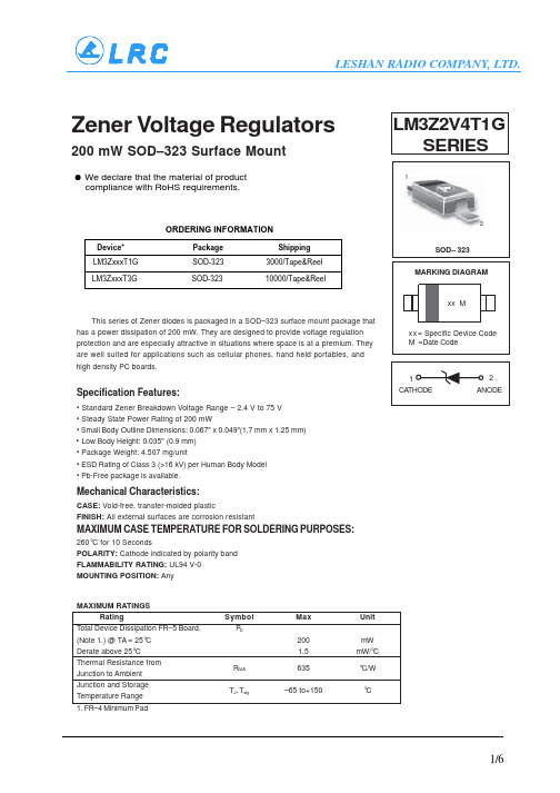
Zener Voltage Regulators200 mW SOD–323 Surface Mount12This series of Zener diodes is packaged in a SOD–323 surface mount package that has a power dissipation of 200 mW. They are designed to provide voltage regulation protection and are especially attractive in situations where space is at a premium. They are well suited for applications such as cellular phones, hand held portables, and high density PC boards.Specification Features:• Standard Zener Breakdown Voltage Range – 2.4 V to 75 V • Steady State Power Rating of 200 mW• Small Body Outline Dimensions: 0.067" x 0.049"(1.7 mm x 1.25 mm).Low Body Height: 0.035" (0.9 mm)• Package Weight: 4.507 mg/unit• ESD Rating of Class 3 (>16 kV) per Human Body Model • Pb-Free package is available.Mechanical Characteristics:CASE:Void-free, transfer-molded plasticFINISH:All external surfaces are corrosion resistantMAXIMUM CASE TEMPERATURE FOR SOLDERING PURPOSES:260°C for 10 SecondsPOLARITY:Cathode indicated by polarity band FLAMMABILITY RATING: UL94 V-0MOUNTING POSITION: AnyMAXIMUM RATINGSRatingSymbol Max Unit Total Device Dissipation FR–5 Board,P D(Note 1.) @ TA = 25°C 200mW Derate above 25°C1.5mW/°C Thermal Resistance from R θJA 635°C/W Junction to AmbientJunction and StorageT J , T stg–65 to+150°CTemperature Range 1. FR–4 Minimum PadORDERING INFORMATIONDevice*Package ShippingLM3ZxxxT1G SOD-3233000/Tape&ReelLM3ZxxxT3GSOD-32310000/Tape&ReelLESHAN RADIO COMPANY, LTD.1/6ƽ We declare that the material of productcompliance with RoHS requirements.LM3Z2V4T1G SERIESELECTRICAL CHARACTERISTICS(T A = 25°C unless otherwise noted,V F = 0.9 V Max. @ I F= 10 mA for all types)Symbol ParameterV Z Reverse Zener Voltage @ I ZT I ZT Reverse CurrentZ ZT Maximum Zener Impedance @ I ZT I ZK Reverse CurrentZ ZK Maximum Zener Impedance @ I ZK I R Reverse Leakage Current @ V R V R Reverse Voltage I F Forward Current V F Forward Voltage @ I FQ V Z Maximum Temperature Coefficient of V Z CMax. Capacitance @V R = 0 and f = 1 MHzLESHAN RADIO COMPANY, LTD.2/6LM3Z2V4T1G SERIES2.Zener voltage is measured with a pulse test current I Z at an ambient temperature of 25°C.LESHAN RADIO COMPANY, LTD.3/6LM3Z2V4T1G SERIESTypical CharacteristicsZ Z T , D Y N A M I C I M P E D A N C E ()Ω1000100101.0C , C A P A C I T A N C E (p F )70V Z , NOMINAL ZENER VOLTAGE (V)Figure 3. Typical Capacitance 104.0V Z , NOMINAL ZENER VOLTAGE (V)Figure 4. Typical Leakage Current70605040302010LESHAN RADIO COMPANY, LTD.4/6LM3Z2V4T1G SERIESTypical Characteristics12V Z , ZENER VOLTAGE (V)100101.00.10.01108.06.04.02.00I Z , Z E N E R C U R R E N T (m A )V Z , ZENER VOLTAGE (V)Figure 5. Zener Voltage versus Zener Current(V Z Up to 12 V)Figure 6. Zener Voltage versus Zener Current(12 V to 75 V)1001010.10.011030507090I Z , Z E N E R C U R R E N T (m A )TEMPERATURE (°C)2501004020PO W E R D I S S I P A T I O N (%)50751001251508060Figure 7. Steady State Power DeratingLESHAN RADIO COMPANY, LTD.5/6PACKAGE DIMENSIONSSOD-323MINMAXMINMAXAB CD E H J K1.601.150.800.250.000.0892.301.801.351.000.400.100.1772.700.0630.0450.0310.0100.00000.00350.0910.0710.0530.0390.0160.0040.00700.106DINMILLIMETERS INCHES0.15 REF 0.006 REF NOTES:1. CONTROLLING DIMENSION: MILLIMETERS2. LEAD THICKNESS SPECIFIED PER L / F DRAWING WITH SOLDER PLATING.DSOD-32312LM3Z2V4T1G SERIESSTYLE 1:PIN 1: CATHODE 2: ANODELESHAN RADIO COMPANY, LTD.6/6Reel DimensionsMetric Dimensions Govern –– English are in parentheses for reference onlyEMBOSSED TAPE AND REEL DATAFOR DISCRETESAT MaxOutside Dimension Measured at EdgeGInside Dimension Measured Near Hub20.2mm Min (.795’’)1.5mm Min(.06’’)13.0mm ± 0.5mm(.512 ±.002’’)50mm Min (1.969’’)Full RadiusSize A Max GT Max 8 mm330mm (12.992’’)8.4mm+1.5mm, -0.0(.33’’+.059’’, -0.00)14.4mm (.56’’)LESHAN RADIO COMPANY, LTD.Storage ConditionsTemperature: 5 to 40 Deg.C (20 to 30 Deg. C is preferred) Humidity: 30 to 80 RH (40 to 60 is preferred )Recommended Period: One year after manufacturing(This recommended period is for the soldering condition only. The characteristics and reliabilities of the products are not restricted to this limitation)元器件交易网Shi p ment S p ecification10 Reel12 Inner Box/Carton 360KPCS/CartonDim(Unit:mm)Dim(Unit:mm)10Reel/Inner Box30KPCS/Inner Box460mm*400mm*420mm8000PCS/Reel (SOT-723,SOD-723)3000PCS/Reel80KPCS/Inner Box (SOT-723,SOD-723)960KPCS/Carton (SOT-723,SOD-723)LESHAN RADIO COMPANY, LTD.元器件交易网。
FK25SM-5中文资料

ELECTRICAL CHARACTERISTICS
Symbol V (BR) DSS V (BR) GSS IGSS IDSS VGS (th) rDS (ON) VDS (ON) yfs Ciss Coss Crss td (on) tr td (off) tf VSD Rth (ch-c) trr Parameter
q
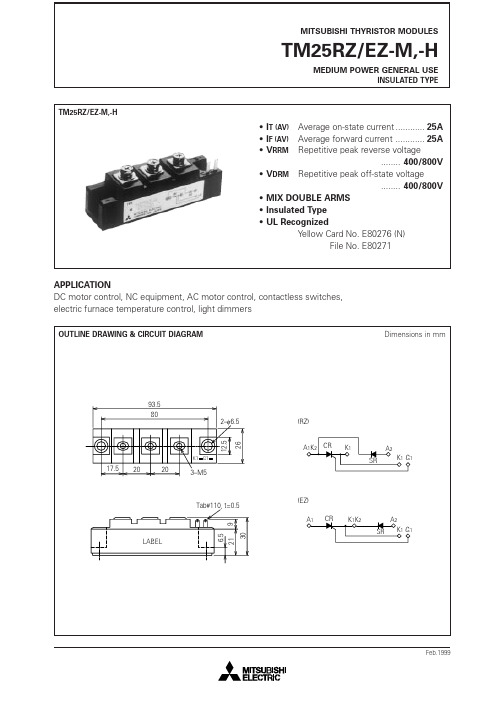
TO-3P
APPLICATION Servo motor drive, Robot, UPS, Inverter Fluorecent lamp, etc.
MAXIMUM RATINGS
Symbol VDSS VGSS ID IDM IS ISM PD Tch Tstg —
(Tc = 25°C)
Parameter Drain-source voltage Gate-source voltage Drain current Drain current (Pulsed) Source current Source current (Pulsed) Maximum power dissipation Channel temperature Storage temperature Weight Typical value VGS = 0V VDS = 0V
Conditions
Ratings 250 ±30 25 75 25 75 250 –55 ~ +150 –55 ~ +150 4.8
Unit V V A A A A W °C °C g
Feb.1999
元器件交易网
MITSUBISHI Nch POWER MOSFET
FK25SM-5
CC2540、BLE、低功耗蓝牙4.0、透传模块-硬件手册

MT254xCoreS 硬件手册V1.0深圳市馒头科技有限公司产品型号说明馒头科技缩写版本编号直插; Board-底板版本更新记录目录第1章产品介绍 (5)1.1蓝牙4.0介绍 (5)1.2MT254xCoreS介绍 (5)第2章硬件资源 (6)2.1晶振 (6)2.2天线 (6)2.3电阻电容 (6)2.4对外接口 (6)第3章技术规格说明 (7)3.1外观尺寸 (7)3.2引脚分布图 (7)3.3引脚功能说明 (8)第4章开发事项 (9)4.1模块透传功能 (9)4.2BLE协议栈开发 (9)4.3IO复用功能表 (10)附录A 模块实物图 (12)第1章产品介绍1.1 蓝牙4.0介绍蓝牙4.0是2012年最新蓝牙版本,是3.0的升级版本;较3.0版本更省电、成本低、3毫秒低延迟、超长有效连接距离、AES-128加密等;通常用在蓝牙耳机、蓝牙音箱等设备上。
蓝牙4.0最重要的特性是省电,极低的运行和待机功耗可以使一粒纽扣电池连续工作数年之久。
此外,低成本和跨厂商互操作性,3毫秒低延迟、AES-128加密等诸多特色,可以用于计步器、心律监视器、智能仪表、传感器物联网等众多领域,大大扩展蓝牙技术的应用范围。
蓝牙4.0已经走向了商用,在最新款的Xperia Z、Galaxy S3、S4、Note2、SurfaceRT、iPhone 5、iPhone 4S、魅族MX3、Moto Droid Razr、HTC One X、小米手机2、The New iPad、iPad 4、MacBook Air、Macbook Pro,Nokia Lumia系列以及台商ACER AS3951系列/Getway NV57系列,ASUS UX21/31三星NOTE系列上都已应用了蓝牙4.0技术。
蓝牙4.0支持两种部署方式:双模式和单模式。
双模式中,低功耗蓝牙功能集成在现有的经典蓝牙控制器中,或再在现有经典蓝牙技术(2.1+EDR/3.0+HS)芯片上增加低功耗堆栈,整体架构基本不变,因此成本增加有限。
LM2578AM资料

LM2578A/LM3578A Switching RegulatorGeneral DescriptionThe LM2578A is a switching regulator which can easily be set up for such DC-to-DC voltage conversion circuits as the buck,boost,and inverting configurations.The LM2578A fea-tures a unique comparator input stage which not only has separate pins for both the inverting and non-inverting inputs, but also provides an internal1.0V reference to each input, thereby simplifying circuit design and p.c.board layout.The output can switch up to750mA and has output pins for its collector and emitter to promote design flexibility.An external current limit terminal may be referenced to either the ground or the V in terminal,depending upon the application.In addi-tion,the LM2578A has an on board oscillator,which sets the switching frequency with a single external capacitor from<1 Hz to100kHz(typical).The LM2578A is an improved version of the LM2578,offer-ing higher maximum ratings for the total supply voltage and output transistor emitter and collector voltages.Featuresn Inverting and non-inverting feedback inputsn 1.0V reference at inputsn Operates from supply voltages of2V to40Vn Output current up to750mA,saturation less than0.9V n Current limit and thermal shut downn Duty cycle up to90%Applicationsn Switching regulators in buck,boost,inverting,and single-ended transformer configurationsn Motor speed controln Lamp flasherConnection Diagram and Ordering InformationDual-In-Line Package00871129Order Number LM3578AM,LM2578AN or LM3578ANSee NS Package Number M08A or N08E February2005LM2578A/LM3578A Switching Regulator©2005National Semiconductor Corporation Functional Diagram00871101L M 2578A /L M 3578A 2Absolute Maximum Ratings(Note1) If Military/Aerospace specified devices are required, please contact the National Semiconductor Sales Office/ Distributors for availability and specifications.Total Supply Voltage50V Collector Output to Ground−0.3V to+50V Emitter Output to Ground(Note2)−1V to+50V Power Dissipation(Note3)Internally limited Output Current750mA Storage Temperature−65˚C to+150˚C Lead Temperature(soldering,10seconds)260˚C Maximum Junction Temperature150˚CESD Tolerance(Note4)2kVOperating RatingsAmbient Temperature RangeLM2578A−40˚C≤T A≤+85˚C LM3578A0˚C≤T A≤+70˚C Junction Temperature RangeLM2578A−40˚C≤T J≤+125˚C LM3578A0˚C≤T J≤+125˚CElectrical CharacteristicsThese specifications apply for2V≤V IN≤40V(2.2V≤V IN≤40V for T J≤−25˚C),timing capacitor C T=3900pF,and25%≤duty cycle≤75%,unless otherwise specified.Values in standard typeface are for T J=25˚C;values in boldface type apply for operation over the specified operating junction temperature range.LM2578A/Symbol Parameter Conditions Typical LM3578A Units(Note5)Limit(Note6) OSCILLATORf OSC Frequency20kHz24kHz(max)16kHz(min)∆f OSC/∆T Frequency Drift with Temperature−0.13%/˚C Amplitude550mV p-p REFERENCE/COMPARATOR(Note7)V R Input Reference I1=I2=0mA and 1.0V Voltage I1=I2=1mA±1%(Note8) 1.050/1.070V(max)0.950/0.930V(min)∆V R/∆V IN Input Reference Voltage LineRegulationI1=I2=0mA and0.003%/VI1=I2=1mA±1%(Note8)0.01/0.02%/V(max) I INV Inverting Input Current I1=I2=0mA,duty cycle=25%0.5µALevel Shift Accuracy Level Shift Current=1mA 1.0%10/13%(max)∆V R/∆t Input Reference Voltage Long TermStability100ppm/1000h OUTPUTV C(sat)Collector Saturation Voltage I C=750mA pulsed,Emittergrounded 0.7V0.90/1.2V(max)V E(sat)Emitter Saturation Voltage I O=80mA pulsed, 1.4VV IN=V C=40V 1.7/2.0V(max)I CES Collector Leakage Current V IN=V CE=40V,Emitter grounded,Output OFF 0.1µA200/250µA(max)BV CEO(SUS)Collector-Emitter Sustaining Voltage I SUST=0.2A(pulsed),V IN=060V50V(min) CURRENT LIMITV CL Sense Voltage Shutdown Level Referred to V IN or Ground110mV(Note9)80mV(min)160mV(max)LM2578A/LM3578A3Electrical Characteristics(Continued)These specifications apply for 2V ≤V IN ≤40V (2.2V ≤V IN ≤40V for T J ≤−25˚C),timing capacitor C T =3900pF,and 25%≤duty cycle ≤75%,unless otherwise specified.Values in standard typeface are for T J =25˚C;values in boldface type apply for operation over the specified operating junction temperature range.LM2578A/Symbol ParameterConditionsTypical LM3578A Units(Note 5)Limit (Note 6)CURRENT LIMIT ∆V CL /∆T Sense Voltage Temperature Drift 0.3%/˚C I CLSense Bias CurrentReferred to V IN 4.0µA Referred to ground0.4µA DEVICE POWER CONSUMPTION I SSupply CurrentOutput OFF,V E =0V2.0mA3.5/4.0mA (max)Output ON,I C =750mA pulsed,14mAV E =0VNote 1:Absolute Maximum Ratings indicate limits beyond which damage to the device may occur.DC and AC electrical specifications do not apply when operating the device beyond its rated operating conditions.Note 2:For T J ≥100˚C,the Emitter pin voltage should not be driven more than 0.6V below ground (see Application Information).Note 3:At elevated temperatures,devices must be derated based on package thermal resistance.The device in the 8-pin DIP must be derated at 95˚C/W,junction to ambient.The device in the surface-mount package must be derated at 150˚C/W,junction-to-ambient.Note 4:Human body model,1.5k Ωin series with 100pF.Note 5:Typical values are for T J =25˚C and represent the most likely parametric norm.Note 6:All limits guaranteed at room temperature (standard type face)and at temperature extremes (bold type face).Room temperature limits are 100%production tested.Limits at temperature extremes are guaranteed via correlation using standard Statistical Quality Control (SQC)methods.All limits are used to calculate AOQL.Note 7:Input terminals are protected from accidental shorts to ground but if external voltages higher than the reference voltage are applied,excessive current will flow and should be limited to less than 5mA.Note 8:I 1and I 2are the external sink currents at the inputs (refer to Test Circuit).Note 9:Connection of a 10k Ωresistor from pin 1to pin 4will drive the duty cycle to its maximum,typically 90%.Applying the minimum Current Limit Sense Voltage to pin 7will not reduce the duty cycle to less than 50%.Applying the maximum Current Limit Sense Voltage to pin 7is certain to reduce the duty cycle below 50%.Increasing this voltage by 15mV may be required to reduce the duty cycle to 0%,when the Collector output swing is 40V or greater (see Ground-Referred Current Limit Sense Voltage typical curve).Typical Performance CharacteristicsOscillator Frequency Changewith TemperatureOscillator Voltage Swing0087113200871133L M 2578A /L M 3578A 4Typical Performance Characteristics(Continued)Input Reference Voltage Drift with TemperatureCollector Saturation Voltage(Sinking Current,Emitter Grounded)0087113400871135Emitter Saturation Voltage(Sourcing Current,Collector at V in )Ground ReferredCurrent Limit Sense Voltage0087113600871137Current Limit Sense Voltage Drift with Temperature Current Limit Response Time for Various Over Drives0087113800871139LM2578A/LM3578A5Typical Performance Characteristics(Continued)Current Limit Sense Voltagevs Supply VoltageSupply Current0087114000871141Supply CurrentCollector Current with Emitter Output Below Ground0087114200871143Test Circuit*Parameter tests can be made using the test circuit shown.Select the desired V in ,collector voltage and duty cycle with adjustable power supplies.A digital volt meter with an input resistance greater than 100M Ωshould be used to measure the following:Input Reference Voltage to Ground;S1in either position.Level Shift Accuracy (%)=(T P3(V)/1V)x 100%;S1at I 1=I 2=1mAInput Current (mA)=(1V −T p3(V))/1M Ω:S1at I 1=I 2=0mA.Oscillator parameters can be measured at T p4using a fre-quency counter or an oscilloscope.The Current Limit Sense Voltage is measured by connecting an adjustable 0-to-1V floating power supply in series with the current limit terminal and referring it to either the ground or the V in terminal.Set the duty cycle to 90%and monitor test point T P5while adjusting the floating power supply voltage until the LM2578A’s duty cycle just reaches 0%.This voltage is the Current Limit Sense Voltage.The Supply Current should be measured with the duty cycle at 0%and S1in the I 1=I 2=0mA position.*LM2578A specifications are measured using automated test equipment.This circuit is provided for the customer’s convenience when checking parameters.Due to possible variations in testing conditions,the measured values from these testing procedures may not match those of the factory.L M 2578A /L M 3578A 6Test Circuit*(Continued)00871103 Op amp supplies are±15VDVM input resistance>100MΩ*LM2578max duty cycle is90%Definition of TermsInput Reference Voltage:The voltage(referred to ground) that must be applied to either the inverting or non-inverting input to cause the regulator switch to change state(ON or OFF).Input Reference Current:The current that must be drawn from either the inverting or non-inverting input to cause the regulator switch to change state(ON or OFF).Input Level Shift Accuracy:This specification determines the output voltage tolerance of a regulator whose output control depends on drawing equal currents from the inverting and non-inverting inputs(see the Inverting Regulator of Fig-ure21,and the RS-232Line Driver Power Supply of Figure 23).Level Shift Accuracy is tested by using two equal-value resistors to draw current from the inverting and non-inverting input terminals,then measuring the percentage difference in the voltages across the resistors that produces a controlled duty cycle at the switch output.Collector Saturation Voltage:With the inverting input ter-minal grounded thru a10kΩresistor and the output transis-tor’s emitter connected to ground,the Collector Saturation-Voltage is the collector-to-emitter voltage for a given collector current.Emitter Saturation Voltage:With the inverting input termi-nal grounded thru a10kΩresistor and the output transistor’s collector connected to V in,the Emitter Saturation Voltage is the collector-to-emitter voltage for a given emitter current. Collector Emitter Sustaining Voltage:The collector-emitter breakdown voltage of the output transistor,mea-sured at a specified current.Current Limit Sense Voltage:The voltage at the CurrentLimit pin,referred to either the supply or the ground terminal,which(via logic circuitry)will cause the output transistor toturn OFF and resets cycle-by-cycle at the oscillator fre-quency.Current Limit Sense Current:The bias current for theCurrent Limit terminal with the applied voltage equal to theCurrent Limit Sense Voltage.Supply Current:The IC power supply current,excluding thecurrent drawn through the output transistor,with the oscilla-tor operating.Functional DescriptionThe LM2578A is a pulse-width modulator designed for useas a switching regulator controller.It may also be used inother applications which require controlled pulse-width volt-age drive.A control signal,usually representing output voltage,fed intothe LM2578A’s comparator is compared with an internally-generated reference.The resulting error signal and the os-cillator’s output are fed to a logic network which determineswhen the output transistor will be turned ON or OFF.Thefollowing is a brief description of the subsections of theLM2578A.COMPARATOR INPUT STAGEThe LM2578A’s comparator input stage is unique in that boththe inverting and non-inverting inputs are available to theuser,and both contain a1.0V reference.This is accom-plished as follows:A1.0V reference is fed into a modifiedvoltage follower circuit(see FUNCTIONAL DIAGRAM).When both input pins are open,no current flows through R1LM2578A/LM3578A7Functional Description(Continued)and R2.Thus,both inputs to the comparator will have the potential of the 1.0V reference,V A .When one input,for example the non-inverting input,is pulled ∆V away from V A ,a current of ∆V/R1will flow through R1.This same current flows through R2,and the comparator sees a total voltage of 2∆V between its inputs.The high gain of the system,through feedback,will correct for this imbalance and return both inputs to the 1.0V level.This unusual comparator input stage increases circuit flex-ibility,while minimizing the total number of external compo-nents required for a voltage regulator system.The inverting switching regulator configuration,for example,can be set up without having to use an external op amp for feedback polarity reversal (see TYPICAL APPLICATIONS).OSCILLATORThe LM2578A provides an on-board oscillator which can be adjusted up to 100kHz.Its frequency is set by a single external capacitor,C 1,as shown in Figure 1,and follows the equationf OSC =8x10⁻⁵/C 1The oscillator provides a blanking pulse to limit maximum duty cycle to 90%,and a reset pulse to the internal circuitry.OUTPUT TRANSISTORThe output transistor is capable of delivering up to 750mA with a saturation voltage of less than 0.9V.(see Collector Saturation Voltage and Emitter Saturation Voltage curves).The emitter must not be pulled more than 1V below ground (this limit is 0.6V for T J ≥100˚C).Because of this limit,an external transistor must be used to develop negative output voltages (see the Inverting Regulator Typical Application).Other configurations may need protection against violation of this limit (see the Emitter Output section of the Applica-tions Information).CURRENT LIMITThe LM2578A’s current limit may be referenced to either the ground or the V in pins,and operates on a cycle-by-cycle basis.The current limit section consists of two comparators:one with its non-inverting input referenced to a voltage 110mV below V in ,the other with its inverting input referenced110mV above ground (see FUNCTIONAL DIAGRAM).The current limit is activated whenever the current limit terminal is pulled 110mV away from either V in or ground.Applications InformationCURRENT LIMITAs mentioned in the functional description,the current limit terminal may be referenced to either the V in or the ground terminal.Resistor R3converts the current to be sensed into a voltage for current limit detection.CURRENT LIMIT TRANSIENT SUPPRESSIONWhen noise spikes and switching transients interfere with proper current limit operation,R1and C1act together as a low pass filter to control the current limit circuitry’s response time.Because the sense current of the current limit terminal varies according to where it is referenced,R1should be less than 2k Ωwhen referenced to ground,and less than 100Ωwhen referenced to V in .00871104FIGURE 1.Value of Timing Capacitor vsOscillator Frequency00871115FIGURE 2.Current Limit,Ground Referred00871116FIGURE 3.Current Limit,V in ReferredL M 2578A /L M 3578A 8Applications Information(Continued)C.L.SENSE VOLTAGE MULTIPLICATIONWhen a larger sense resistor value is desired,the voltage divider network,consisting of R1and R2,may be used.This effectively multiplies the sense voltage by(1+R1/R2).Also, R1can be replaced by a diode to increase current limit sense voltage to about800mV(diode V f+110mV).UNDER-VOLTAGE LOCKOUTUnder-voltage lockout is accomplished with few external components.When V in becomes lower than the zener breakdown voltage,the output transistor is turned off.This occurs because diode D1will then become forward biased, allowing resistor R3to sink a greater current from the non-inverting input than is sunk by the parallel combination of R1 and R2at the inverting terminal.R3should be one-fifth of the value of R1and R2in parallel.MAXIMUM DUTY CYCLE LIMITINGThe maximum duty cycle can be externally limited by adjust-ing the charge to discharge ratio of the oscillator capacitor with a single external resistor.Typical values are50µA for the charge current,450µA for the discharge current,and a voltage swing from200mV to750mV.Therefore,R1is selected for the desired charging and discharging slopes and C1is readjusted to set the oscillator frequency.00871117 FIGURE4.Current Limit Transient Suppressor,Ground Referred00871118 FIGURE5.Current Limit Transient Suppressor,V in Referred00871119 FIGURE6.Current Limit Sense Voltage Multiplication,Ground Referred00871120FIGURE7.Current Limit Sense Voltage Multiplication,V in Referred00871122FIGURE8.Under-Voltage LockoutLM2578A/LM3578A9Applications Information(Continued)DUTY CYCLE ADJUSTMENTWhen manual or mechanical selection of the output transis-tor’s duty cycle is needed,the cirucit shown below may be used.The output will turn on with the beginning of each oscillator cycle and turn off when the current sunk by R2and R3from the non-inverting terminal becomes greater than the current sunk from the inverting terminal.With the resistor values as shown,R3can be used to adjust the duty cycle from 0%to 90%.When the sum of R2and R3is twice the value of R1,the duty cycle will be about 50%.C1may be a large electrolytic capacitor to lower the oscillator frequency below 1Hz.REMOTE SHUTDOWNThe LM2578A may be remotely shutdown by sinking a greater current from the non-inverting input than from the inverting input.This may be accomplished by selecting re-sistor R3to be approximately one-half the value of R1and R2in parallel.EMITTER OUTPUTWhen the LM2578A output transistor is in the OFF state,if the Emitter output swings below the ground pin voltage,the output transistor will turn ON because its base is clamped near ground.The Collector Current with Emitter Output Be-low Ground curve shows the amount of Collector current drawn in this mode,vs temperature and Emitter voltage.When the Collector-Emitter voltage is high,this current will cause high power dissipation in the output transistor and should be avoided.This situation can occur in the high-current high-voltage buck application if the Emitter output is used and the catch diode’s forward voltage drop is greater than 0.6V.A fast-recovery diode can be added in series with the Emitter output to counter the forward voltage drop of the catch diode (see Figure 2).For better efficiency of a high output current buck regulator,an external PNP transistor should be used as shown in Figure 16.SYNCHRONIZING DEVICESWhen several devices are to be operated at once,their oscillators may be synchronized by the application of an external signal.This drive signal should be a pulse waveform with a minimum pulse width of 2µs.and an amplitude from00871121FIGURE 9.Maximum Duty Cycle Limiting00871123FIGURE 10.Duty Cycle Adjustment00871124FIGURE 11.Shutdown Occurs when V L is High00871130FIGURE 12.D1Prevents Output Transistor from Improperly Turning ON due to D2’s Forward Voltage L M 2578A /L M 3578A 10Applications Information(Continued)1.5V to2.0V.The signal source must be capable of 1.)driving capacitive loads and 2.)delivering up to 500µA for each LM2578A.Capacitors C1thru CN are to be selected for a 20%slower frequency than the synchronization frequency.Typical ApplicationsThe LM2578A may be operated in either the continuous or the discontinuous conduction mode.The following applica-tions (except for the Buck-Boost Regulator)are designed for continuous conduction operation.That is,the inductor cur-rent is not allowed to fall to zero.This mode of operation has higher efficiency and lower EMI characteristics than the dis-continuous mode.BUCK REGULATORThe buck configuration is used to step an input voltage down to a lower level.Transistor Q1in Figure 14chops the input DC voltage into a squarewave.This squarewave is then converted back into a DC voltage of lower magnitude by the low pass filter consisting of L1and C1.The duty cycle,D,of the squarewave relates the output voltage to the input volt-age by the following equation:V out =D x V in =V in x (t on )/(t on +t off ).Figure 15is a 15V to 5V buck regulator with an output current,I o ,of 350mA.The circuit becomes discontinuous at 20%of I o(max),has 10mV of output voltage ripple,an effi-ciency of 75%,a load regulation of 30mV (70mA to 350mA)and a line regulation of 10mV (12≤V in ≤18V).Component values are selected as follows:R1=(V o −1)x R2where R2=10k ΩR3=V/I sw(max)R3=0.15Ωwhere:V is the current limit sense voltage,0.11VI sw(max)is the maximum allowable current thru the output transistor.L1is the inductor and may be found from the inductance calculation chart (Figure 16)as follows:Given V in =15VV o =5VI o(max)=350mA f OSC =50kHzDiscontinuous at 20%of I o(max).Note that since the circuit will become discontinuous at 20%of I o(max),the load current must not be allowed to fall below 70mA.00871125FIGURE 13.Synchronizing Devices00871105FIGURE 14.Basic Buck RegulatorLM2578A/LM3578A11Typical Applications(Continued)00871106V in =15V R3=0.15ΩV o =5V C1=1820pF V ripple =10mV C2=220µF I o =350mA C3=20pF f osc =50kHz L1=470µH R1=40k ΩD1=1N5818R2=10k ΩFIGURE 15.Buck or Step-Down RegulatorL M 2578A /L M 3578A 12LM2578A/LM3578A Typical Applications(Continued)00871131FIGURE16.DC/DC Inductance Calculator13Typical Applications(Continued)Step 1:Calculate the maximum DC current through the inductor,I L(max).The necessary equations are indicated at the top of the chart and show that I L(max)=I o(max)for the buck configuration.Thus,I L(max)=350mA.Step 2:Calculate the inductor Volts-sec product,E-T op ,according to the equations given from the chart.For the Buck:E-T op =(V in −V o )(V o /V in )(1000/f osc )=(15−5)(5/15)(1000/50)=66V-µs.with the oscillator frequency,f osc ,expressed in kHz.Step 3:Using the graph with axis labeled “Discontinuous At %I OUT ”and “I L(max,DC)”find the point where the desired maximum inductor current,I L(max,DC)intercepts the desired discontinuity percentage.In this example,the point of interest is where the 0.35A line intersects with the 20%line.This is nearly the midpoint of the horizontal axis.Step 4:This last step is merely the translation of the point found in Step 3to the graph directly below it.This is accom-plished by moving straight down the page to the point which intercepts the desired E-T op .For this example,E-T op is 66V-µs and the desired inductor value is 470µH.Since this example was for 20%discontinuity,the bottom chart could have been used directly,as noted in step 3of the chart instructions.For a full line of standard inductor values,contact Pulse Engineering (San Diego,Calif.)regarding their PE526XX series,or A.I.E.Magnetics (Nashville,Tenn.).A more precise inductance value may be calculated for the Buck,Boost and Inverting Regulators as follows:BUCKL =V o (V in −V o )/(∆I L V in f osc )BOOSTL =V in (V o −V in )/(∆I L f osc V o )INVERTL =V in |V o |/[∆I L (V in +|V o |)f osc ]where ∆I L is the current ripple through the inductor.∆I L is usually chosen based on the minimum load current expected of the circuit.For the buck regulator,since the inductor current I L equals the load current I O ,∆I L =2•I O(min)∆I L =140mA for this circuit.∆I L can also be interpreted as ∆I L =2•(Discontinuity Factor)•I Lwhere the Discontinuity Factor is the ratio of the minimum load current to the maximum load current.For this example,the Discontinuity Factor is 0.2.The remainder of the components of Figure 15are chosen as follows:C1is the timing capacitor found in Figure 1.C2≥V o (V in −V o )/(8f osc 2V in V ripple L1)where V ripple is the peak-to-peak output voltage ripple.C3is necessary for continuous operation and is generally in the 10pF to 30pF range.D1should be a Schottky type diode,such as the 1N5818or 1N5819.BUCK WITH BOOSTED OUTPUT CURRENTFor applications requiring a large output current,an external transistor may be used as shown in Figure 17.This circuit steps a 15V supply down to 5V with 1.5A of output current.The output ripple is 50mV,with an efficiency of 80%,a load regulation of 40mV (150mA to 1.5A),and a line regulation of 20mV (12V ≤V in ≤18V).Component values are selected as outlined for the buck regulator with a discontinuity factor of 10%,with the addition of R4and R5:R4=10V BE1B f /I pR5=(V in −V −V BE1−V sat )B f /(I L(max,DC)+I R4)where:V BE1is the V BE of transistor Q1.V sat is the saturation voltage of the LM2578A output transis-tor.V is the current limit sense voltage.B f is the forced current gain of transistor Q1(B f =30for Figure 17).I R4=V BE1/R4I p =I L(max,DC)+0.5∆I LL M 2578A /L M 3578A 14Typical Applications(Continued)BOOST REGULATORThe boost regulator converts a low input voltage into a higher output voltage.The basic configuration is shown in Figure 18.Energy is stored in the inductor while the transis-tor is on and then transferred with the input voltage to the output capacitor for filtering when the transistor is off.Thus,V o =V in +V in (t on /t off ).The circuit of Figure 19converts a 5V supply into a 15V supply with 150mA of output current,a load regulation of 14mV (30mA to 140mA),and a line regulation of 35mV (4.5V ≤V in ≤8.5V).R1=(V o −1)R2where R2=10k Ω.R3=V/(I L(max,DC)+0.5∆I L )where:∆I L =2(I LOAD(min))(V o /V in )∆I L is 200mA in this example.R4,C3and C4are necessary for continuous operation and are typically 220k Ω,20pF,and 0.0022µF respectively.C1is the timing capacitor found in Figure 1.C2≥I o (V o −V in )/(f osc V o V ripple ).00871108V in =15V R4=200ΩV o =5V R5=330ΩV ripple =50mV C1=1820pF I o =1.5AC2=330µFf osc =50kHz C3=20pF R1=40k ΩL1=220µH R2=10k ΩD1=1N5819R3=0.05ΩQ1=D45FIGURE 17.Buck Converter with Boosted Output Current00871109FIGURE 18.Basic Boost Regulator00871111V in =5V R4=200k ΩV o =15V C1=1820pF V ripple =10mV C2=470µF I o =140mA C3=20pF f osc =50kHz C4=0.0022µF R1=140k ΩL1=330µH R2=10k ΩD1=1N5818R3=0.15ΩFIGURE 19.Boost or Step-Up RegulatorLM2578A/LM3578A15Typical Applications(Continued)D1is a Schottky type diode such as a 1N5818or 1N5819.L1is found as described in the buck converter section,using the inductance chart for Figure 16for the boost configuration and 20%discontinuity.INVERTING REGULATORFigure 20shows the basic configuration for an inverting regulator.The input voltage is of a positive polarity,but the output is negative.The output may be less than,equal to,or greater in magnitude than the input.The relationship be-tween the magnitude of the input voltage and the output voltage is V o =V in x (t on /t off ).Figure 21shows an LM2578A configured as a 5V to −15V polarity inverter with an output current of 300mA,a load regulation of 44mV (60mA to 300mA)and a line regulation of 50mV (4.5V ≤V in ≤8.5V).R1=(|V o |+1)R2where R2=10k Ω.R3=V/(I L(max,DC)+0.5∆I L ).R4=10V BE1B f /(I L (max,DC)+0.5∆I L )where:V,V BE1,V sat ,and B f are defined in the “Buck Converter with Boosted Output Current”section.∆I L =2(I LOAD(min))(V in +|V o |)/V INR5is defined in the “Buck with Boosted Output Current”section.R6serves the same purpose as R4in the Boost Regulator circuit and is typically 220k Ω.C1,C3and C4are defined in the “Boost Regulator”section.C2≥I o |V o |/[f osc (|V o |+V in )V ripple ]L1is found as outlined in the section on buck converters,using the inductance chart of Figure 16for the invert con-figuration and 20%discontinuity.BUCK-BOOST REGULATORThe Buck-Boost Regulator,shown in Figure 22,may step a voltage up or down,depending upon whether or not the desired output voltage is greater or less than the input voltage.In this case,the output voltage is 12V with an input voltage from 9V to 15V.The circuit exhibits an efficiency of 75%,with a load regulation of 60mV (10mA to 100mA)and a line regulation of 52mV.R1=(V o −1)R2where R2=10k ΩR3=V/0.75AR4,C1,C3and C4are defined in the “Boost Regulator”section.D1and D2are Schottky type diodes such as the 1N5818or 1N5819.where:V d is the forward voltage drop of the diodes.V sat is the saturation voltage of the LM2578A output transis-tor.V sat1is the saturation voltage of transistor Q1.L1≥(V in −V sat −V sat1)(t on /I p )00871110FIGURE 20.Basic Inverting Regulator00871112V in =5V R4=190ΩV o =−15V R5=82ΩV ripple =5mV R6=220k ΩI o =300mA C1=1820pF I min =60mAC2=1000µFf osc =50kHz C3=20pF R1=160k ΩC4=0.0022µF R2=10k ΩL1=150µH R3=0.01ΩD1=1N5818FIGURE 21.Inverting RegulatorL M 2578A /L M 3578A16。
TM25RZ-H资料
ABSOLUTE MAXIMUM RATINGSUnit V V V V V VINSULATED TYPEM 400480320400480320H 800960640800960640Symbol V RRM V RSM V R (DC)V DRM V DSM V D (DC)ParameterRepetitive peak reverse voltage Non-repetitive peak reverse voltage DC reverse voltageRepetitive peak off-state voltage Non-repetitive peak off-state voltage DC off-state voltageUnit A A A A 2s A/µs W W V V A °C °C V N·m kg·cm N·m kg·cm gConditionsSingle-phase, half-wave 180° conduction, T C =93°C One half cycle at 60Hz, peak value Value for one cycle of surge current V D =1/2V DRM , I G =0.5A, T j =125°CCharged part to case Main terminal screw M5Mounting screw M6Typical valueRatings 39255001.0 × 1031005.00.5105.02.0–40~125–40~12525001.47~1.9615~201.96~2.9420~30160Symbol I T (RMS), I F (RMS)I T (AV), I F (AV)I TSM , I FSM I 2t di/dt P GM P G (AV)V FGM V RGM I FGM T j T stg V iso——ParameterRMS current Average currentSurge (non-repetitive) current I 2t for fusingCritical rate of rise of on-state current Peak gate power dissipation Average gate power dissipation Peak gate forward voltage Peak gate reverse voltage Peak gate forward current Junction temperature Storage temperature Isolation voltageMounting torqueWeight Voltage classELECTRICAL CHARACTERISTICSUnit mA mA V V/µs V V mA °C/W °C/W M ΩLimitsSymbol I RRM I DRM V TM , V FM dv/dt V GT V GD I GT R th (j-c)R th (c-f)—ParameterRepetitive peak reverse current Repetitive peak off-state current Foward voltageCritical rate of rise of off-state voltage Gate trigger voltage Gate non-trigger voltage Gate trigger current Thermal resistance Contact thermal resistance Insulation resistanceTest conditionsT j =125°C, V RRM applied T j =125°C, V DRM appliedT j =125°C, I TM =I FM =75A, instantaneous meas.T j =125°C, V D =2/3V DRM T j =25°C, V D =6V, R L =2ΩT j =125°C, V D =1/2V DRM T j =25°C, V D =6V, R L =2ΩJunction to case (per 1/2 module)Case to fin, conductive grease applied (per 1/2 module)Measured with a 500V megohmmeter between main terminal and caseMin.———500—0.2510——10Typ.——————————Max.4.04.01.5—3.0—500.80.2—Note:Items of the above table applies to the Thyristor part and the Diode part as circled in the following tables.INSULATED TYPEINSULATED TYPEINSULATED TYPE。
SG3525AN中文资料

. LATCHING PWM TO PREVENT MULTIPLE PULSES
. DUAL SOURCE/SINK OUTPUT DRIVERS
DIP16
16(Narrow)
DESCRIPTION
The SG3525Aseries of pulse width modulator integrated circuits are designed to offer improved performance and lowered external parts count when used in designing all types of switching power supplies. The on-chip + 5.1 V reference is trimmed to ± 1 % and the input common-mode range of the error amplifier includes the reference voltage eliminating external resistors. A sync input to the oscillator allows multiple units to be slaved or a single unit to be synchronized to an external system clock. A single resistor betweenthe CT andthe dischargeterminals provide a wide range of dead time ad- justment. Thesedevicesalso featurebuilt-insoft-startcircuitry with only an external timing capacitor required. A shutdownterminal controls both the soft-start circuity and the output stages, providing instantaneous
TMX320C6211BGLW100资料

Table of Contents GHK BGA package (bottom view) . . . . . . . . . . . . . . . . . . . 3 description . . . . . . . . . . . . . . . . . . . . . . . . . . . . . . . . . . . . . . . 4 device characteristics . . . . . . . . . . . . . . . . . . . . . . . . . . . . . . 5 functional and CPU (DSP core) block diagram . . . . . . . . . 6 CPU (DSP core) description . . . . . . . . . . . . . . . . . . . . . . . . 7 memory map summary . . . . . . . . . . . . . . . . . . . . . . . . . . . . . 9 signal groups description . . . . . . . . . . . . . . . . . . . . . . . . . . 10 signal descriptions . . . . . . . . . . . . . . . . . . . . . . . . . . . . . . . . development support . . . . . . . . . . . . . . . . . . . . . . . . . . . . . . documentation support . . . . . . . . . . . . . . . . . . . . . . . . . . . . clock PLL . . . . . . . . . . . . . . . . . . . . . . . . . . . . . . . . . . . . . . . power-down mode logic . . . . . . . . . . . . . . . . . . . . . . . . . . . power-supply sequencing . . . . . . . . . . . . . . . . . . . . . . . . . . absolute maximum ratings over operating case temperature range . . . . . . . . . . . . . . . . . . . . . . . . . . . recommended operating conditions . . . . . . . . . . . . . . . . . recommended operating conditions (PCI only) . . . . . . . . electrical characteristics over recommended rangesof supply voltage and operating case temperature . . . . . . . . . . . . . . . . . . . . . . . . . . . . electrical characteristics over recommended ranges of supply voltage and operating case temperature (PCI only) . . . . . . . . . . . . . . . . . . . . . . . 13 22 25 26 28 31 32 32 32 33 33 parameter measurement information . . . . . . . . . . . . . . . 34 input and output clocks . . . . . . . . . . . . . . . . . . . . . . . . . . . 35 asynchronous memory timing . . . . . . . . . . . . . . . . . . . . . 37 synchronous-burst memory timing . . . . . . . . . . . . . . . . . 40 synchronous DRAM timing . . . . . . . . . . . . . . . . . . . . . . . . 42 HOLD/HOLDA timing . . . . . . . . . . . . . . . . . . . . . . . . . . . . 46 reset timing . . . . . . . . . . . . . . . . . . . . . . . . . . . . . . . . . . . . . 47 external interrupt timing . . . . . . . . . . . . . . . . . . . . . . . . . . 49 PCI I/O timings . . . . . . . . . . . . . . . . . . . . . . . . . . . . . . . . . . 50 PCI reset timing . . . . . . . . . . . . . . . . . . . . . . . . . . . . . . . . . 51 PCI serial EEPROM interface timing . . . . . . . . . . . . . . . 52 multichannel buffered serial port timing . . . . . . . . . . . . . 53 DMAC, timer, power-down timing . . . . . . . . . . . . . . . . . . 63 JTAG test-port timing . . . . . . . . . . . . . . . . . . . . . . . . . . . . 65 mechanical data . . . . . . . . . . . . . . . . . . . . . . . . . . . . . . . . . 66 revision history . . . . . . . . . . . . . . . . . . . . . . . . . . . . . . . . . . 67
MAX3225中文资料
Ordering Information continued at end of data sheet.
_____________________ Selector Guide
PART NO. OF GUARANTEED AUTOREADY DRIVERS/ DATA RATE SHUTDOWN OUTPUT RECEIVERS (bps) PLUS 2/2 2/2 1/1 1/1 3/5 3/5 250k 1M 250k 1M 250k 1M — —
MAX3224–MAX3227/MAX3244/MAX3245 †
_______________Ordering Information
PART MAX3224CPP MAX3224CAP MAX3224EPP MAX3224EAP MAX3225CPP MAX3225CAP MAX3225EPP MAX3225EAP TEMP. RANGE 0°C to +70°C 0°C to +70°C -40°C to +85°C -40°C to +85°C 0°C to +70°C 0°C to +70°C -40°C to +85°C -40°C to +85°C PIN-PACKAGE 20 Plastic DIP 20 SSOP 20 Plastic DIP 20 SSOP 20 Plastic DIP 20 SSOP 20 Plastic DIP 20 SSOP
________________________Applications
Notebook, Subnotebook, and Palmtop Computers Cellular Phones Battery-Powered Equipment Hand-Held Equipment Peripherals Printers