HZ11A1中文资料
MT2011中文资料

P R E L I M I N A R YRF SILICON AND SUBSYSTEMS SOLUTIONSFOR BROADBAND COMMUNICATIONS AND AUTOMOTIVE ELECTRONICSMICROTUNER™ MT2011 SINGLE-CHIP BROADBAND TUNER PRODUCT BRIEFThe MicroTuner MT2011 is a fully integrated single-chip tuner, optimized for digital OpenCable compliant STB applications.MT2011 Single-Chip Broadband Tuner元器件交易网MT2011 SINGLE-CHIP BROADBAND TUNERPRODUCT BRIEFMT2011PB-00070 — Rev 1.0January 2008P R E L I M I N A R YMicrotune, Inc., 2201 10th Street, Plano, TX 75074, USATel: +1-972-673-1600, Fax: +1-972-673-1602, E-mail: sales@, Web site: For a detailed list of office locations, sales offices, and sales representatives, visit our web site at Microtune believes that the information in this document is accurate and reliable, as of the date of this document. Microtune assumes no responsibility for any consequences arising from the use of this information, nor from any infringement of patents or the rights of third parties which may result from its use. No license is granted by implication or otherwise under any patent or other rights of Microtune. The information in this publication replaces and supersedes all information previously supplied, and is subject to change without notice. The customer is responsible for assuring that proper design and operating safeguards are observed to minimize inherent and procedural hazards. Microtune assumes no responsibility for applications assistance or customer product design.The devices described in this document are not authorized for use in medical, life-support equipment, or any other application involving a potential risk of severe property or environmental damage, personal injury, or death without prior express written approval of Microtune. Any such use is understood to be entirely at the user’s risk.Microtune is a registered trademark of Microtune, Inc. MicroTuner, MicroStreamer, VideoCaster, DataCaster, ClearTune, and the Microtune logo are trademarks of Microtune, Inc. All other trademarks belong to their respective companies.Microtune’s products are protected by one or more of the following U.S. patents: 5,625,325; 5,648,744; 5,717,730; 5,737,035; 5,739,730; 5,805,988; 5,847,612; 6,100,761; 6,104,242; 6,163,684; 6,169,569; 6,172,378; 6,177,964; 6,211,745; 6,218,899; 6,268,778; 6,310,387; 6,323,736; 6,355,537; 6,429,502; 6,462,327; 6,535,068; 6,580,313; 6,608,522; 6,631,257; 6,714,776; 6,725,463; 6,744,308; 6,771,124; 6,784,945; 6,804,099; 6,888,406; 6,891,435; 6,906,594; 6,909,886; 6,919,774; 6,920,182; 6,922,556; 6,963,478; 6,973,288; 6,993,310; 7,035,614; 7,078,960; 7,079,195; 7,164,899; 7,171,176; 7,184,724; 7,190,942; 7,190,943; D469,742 and additional patents pending or filed.Entire contents Copyright © 1996 - 2008 Microtune, Inc. 062007RECOMMENDED OPERATING CONDITIONSP ARAMETERM IN T YP M AX U NIT Input frequency range 481000MHzSecond intermediate center frequency (programmable) 30 57 MHz Supply voltage, +3.3 V 3.15 3.3 3.45 V Supply voltage, +5 V 4.75 5.0 5.25 V Supply voltage ripple15mVp-pOperating junction temperature 125 °C VGA differential output load impedance 300 Ω Serial control clock400kHzDNC differential load impedance800ΩABSOLUTE MAXIMUM RATINGSP ARAMETERM IN M AX U NIT Supply voltage, +3.3 V 3.6 V Supply voltage, +5 V6VStorage temperature range -50 +150 °C Lead Free solder temperature (5 seconds, 3 reps.)+260°CTUNER ELECTRICAL CHARACTERISTICSP ARAMETERM IN T YP M AX U NIT Power SupplyActive current, 3.3 V 82 mA Active current, 5 V 270 mA RF Signal PathInput frequency range 48 1000 MHz Noise figure (DNC Out)10.5dBTerminal voltage gain (DNC Out) 39 dBRF AGC range (0 to 3.3 V)1 30 dB Image rejection 75dBc LO phase noise (1 kHz)-75 dBc/Hz LO phase noise (10 kHz)-85dBc/HzLO phase noise (100 kHz)48 MHz to 860 MHz -105 dBc/Hz LO phase noise (100 kHz) 860 MHz to 1000 MHz -104 dBc/HzLO step size2 kHz IF VGAFrequency range 30 57 MHzOutput voltage swing1.0Vp-pTerminal voltage gain,VGACTRL = 0.7 to 3.3 V <12.5 >51.5 dBIF AGC range39DbFDC Frequency Range 70 130 MHz Gain 1 dB Noise Figure12dB1Note: With Microtune attenuator designMT2011 Block DiagramMT2011 Pin DiagramOutA 1 D V C C L O 1 S e r C L K S e r D a t a S e r V C C X T A L n X T A L p S R O V C C S R O O U T D V C C L O 2 V G A O U T p V G A O U T n V G A V C C V G A V C C A G C C T R LD N C I N nD N C I N pD N C V C C r fG N DU P C O U T nU P C O U T pG N DU P C V C CU P C V C CN CG N DR F i n nDNCOUTnG N D元器件交易网。
IC-R71E 收信机 收信机中文操作手册(原版翻译)
30MHz)
选择性
SSB CW RTTY CW-N RTTY-N AM FM
-6dB 时 2.3KHz (最小可调 500Hz) -60dB 时 4.2KHZ -6dB 时 500Hz -60dB 时 1.5KHZ -6dB 时 6KHz (最小可调 2.7KHz) -50dB 时 15KHZ -6dB 时 15KHz -60dB 时 25KHZ
优异的接收性能
应用 ICOM 开发的毫瓦分贝 J-FET IC-R71 具有 105dB 的动态范围 70.4515MHz 的第一中频实际上 消除了寄生噪声影响 加上使用了 ICOM 通带调谐技术 PBT 的高增益 9.0115MHz 第二中频 一个深度 的中频陷波器 可调的自动增益和噪音消隐 可用于调节消除脉冲噪音 音频音调调节控制 即使在 存在强干扰或高噪声水平情况下都可清晰接收
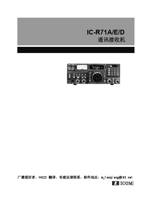
IC-R71A/E/D
通讯接收机 使用手册
广播爱好者 m222 翻译 有建议请联系 邮件地址 m_fanqiang@
目录
第一章 技术规格........................................................1 第二章 功能特性........................................................2 第三章 安装............................................................3 第四章 操作控制装置....................................................4 第五章 操作说明........................................................9 附录 1 IC-R71E 前面板图..................................................18
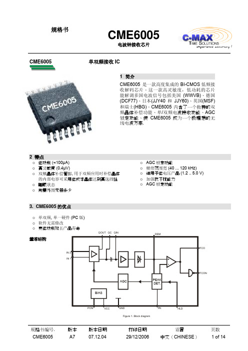
电波表芯片CME6005中文资料
语言 中文(CHINESE)
页数 1 of 14
规格书 CME6005
C-MAX TimeSolutions
7 电器参数
V CC
=
3V,
输入信号频率
77.5
kHz
+/-
5
Hz;
载波电压从
100%
减至
25%
历时
最大
tMOD
=
200ms;
tamb
=
25°C,
最大/最小值测于摄氏 +25 度, 另有说明除外.
12 DEM 11 HLD 10 PK 9 PON
8 TCO
7
TCON
Figure 2. Pad layout
Th e PA D co or d in a te s are referred to the left bottom point of the contact window
QC 1
16 NC
打印日期 29/12/2006
语言 中文(CHINESE)
页数 1 of 14
规格书 CME6005
C-MAX TimeSolutions
6 裸片引脚定义图
SSO16 封装引脚定义图
LinkTrack AOA 用户手册 V1.1 (中文)说明书
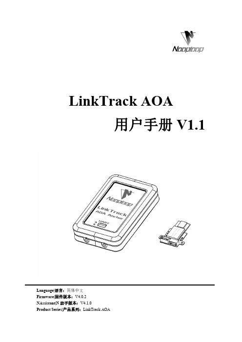
LinkTrack AOA用户手册V1.1Language|语言:简体中文Firmware|固件版本:V4.0.2NAssistant|N助手版本:V4.1.0Product Series|产品系列:LinkTrack AOAContent|目录LinkTrack AOA (1)用户手册V1.1 (1)Content|目录 (2)Disclaimer|免责声明 (4)1Introduction|介绍 (5)2Basic Introduction|基础介绍 (6)2.1Node Installation|节点安装 (6)2.2About the Antenna|关于天线 (6)2.3About the Obstruction|关于障碍物 (6)3AOA Quick Start|AOA快速入门 (7)3.1Introduction|介绍 (7)3.2Steps|步骤 (7)3.3Precautions|注意事项 (9)4NAssistant Operations|NAssistant操作 (10)4.1Quick Start|快速使用 (10)4.2Firmware Update|固件更新 (10)4.3Record,Replay and Export|录制、回放与导出 (10)5Variable|变量 (11)5.1Dis|距离 (11)5.2Angle|角度 (11)5.3RSSI|信号强度指示 (11)5.4Valid Node Quantity|有效节点数 (11)5.5Role&ID|角色与ID (12)5.6Data Length&Data|数据长度与数据 (12)5.7Time|时间 (12)5.8Voltage|供电电压 (12)6Protocol Unpack|协议解析 (13)6.1NLink Protocol|NLink协议 (13)6.1.1Introduction|介绍 (13)6.1.2Protocol Content|协议内容 (14)6.1.3Example|示例 (15)6.1.3.1T端采集的NLink_LinkTrack_AOA_Node_Frame0 (15)6.1.3.2A0端采集的NLink_LinkTrack_AOA_Node_Frame0 (17)6.1.3.3M端采集的NLink_LinkTrack_AOA_Node_Frame0 (18)6.1.3.4A0端采集的NLink_LinkTrack_Node_Frame0 (19)6.1.3.5T端采集的NLink_LinkTrack_Node_Frame0 (20)7How to Deal with|如何处理问题 (21)7.1Read Manuals Carefully|仔细阅读手册 (21)7.2Poor Performan and Abnormal Analysis|性能不佳与异常分析 (21)7.3Feasibility Analysis|可行性分析 (21)8FAQ|常见问题解答 (22)9Abbreviation and Acronyms|简写与首字母缩略 (24)10Reference|参考 (25)11Update Log|更新日志 (26)12Further Information|更多信息 (27)Disclaimer|免责声明Disclaimer|免责声明Document Information|文档信息Nooploop reserves the right to change product specifications without notice.As far as possible changes to functionality and specifications will be issued in product specific errata sheets or in new versions of this document.Customers are advised to check with Nooploop for the most recent updates on this product.Nooploop保留更改产品规格的权利,恕不另行通知。
PT2256中文资料

簡介PT2256是一個使用CMOS製程技術,且專為音響設備設計而成的音量控制IC。
PT2256內建左、右兩聲道,適用於單音(mono)及立體聲(stereo)的聲音處理,且提供較寬頻的回應範圍及低諧波失真的特性。
另外,PT2256不僅僅只有單純的音量控制,同時也提供了響度(Loudness)的音質效果,使得簡單中又多了一份色彩。
特性• CMOS技術•低消耗功率•簡化外部元件•具有寬廣的工作電壓範圍4.5V∼12V(Backup需4.5V以上)•衰減值範圍0dB∼-78dB,其控制藉由UP、Down pin處理• IC內建8段獨立直流電壓輸出準位•響度電路(Loudness Circuit)可提供20dB增益•提供寬頻的回應範圍及低諧波失真•包裝可分為DIP16及SOP16應用範圍•音響方面的音量控制方塊圖腳位配置圖腳位敘述腳位編號 腳位名稱 輸入/輸出說明 1 VSS -負電源輸入端 2 OUT1 O左聲道音源輸出端 3 IN1 I左聲道音源輸入端 4 LT1 O 響度(Loudness)輸出端 5 AGND -類比接地 6 /UP I音量上升控制輸入端,每按一次鍵上升一階。
(內建Pull-up 電阻)7 /DN I音量下降控制輸入端,每按一次鍵下降一階。
(內建Pull-up 電阻)8 OSC I/O由R-C 電路所組合成的振盪方式,當有按鍵按下時才有振盪產生。
9 /RST I初始值設定腳位,若此為低電壓準位輸入時,則初始值設定為-46dB 。
(內建Pull-up 電阻)10 /INH I禁能腳位,若此為低電壓準位輸入時,則IC 內部所有運作停止。
11 DCO O 直流電壓準位輸出端。
(內建8階直流電壓輸出) 12 AGND -類比接地 13 LT2 O響度(Loudness)輸出端 14 IN2 I右聲道音源輸入端 15 OUT2 O右聲道音源輸出端 16 VDD - 正電源輸入端功能敘述衰減動作PT2256是由內部梯狀電阻與外部按鍵控制來加以改變音量的變化,且響度(Loudness)的動作是在Step 10(-20dB)後才有明顯的表現。
LC245A中文资料
GQN OR ZQN PACKAGE (TOP VIEW)
1234
A B C D E
TERMINAL ASSIGNMENTS
1
2
3
4
A
A1
DIR
VCC
OE
B
A3
B2
A2
B1
C
A5
A4
B4
B3
D
A7
B6
A6
B5
E
GND
A8
B8
B7
FUNCTION TABLE
INPUTS
OE DIR
L
L
L
H
H
X
OPERATION
QFN – RGY
Reel of 1000
SN74LVC245ARGYR
SOIC – DW
Tube of 25 Reel of 2000
SN74LVC245ADW SN74LVC245ADWR
SOP – NS
Reel of 2000
SN74LVC245ANSR
SSOP – DB
Reel of 2000
Please be aware that an important notice concerning availability, standard warranty, and use in critical applications of Texas Instruments semiconductor products and disclaimers thereto appears at the end of this data sheet.
DIR 1 A1 2 A2 3 A3 4 A4 5 A5 6 A6 7 A7 8 A8 9 GND 10
PLE11-0中文资料

Exceptionally reliable general purposerelayLong life (minimum 100,000 electricaloperations) assured by silver contacts Built-in operation indicator (mechanical,LED), diode surge suppression, Varistorsurge suppressionThe contact operation can be easily checked by mechanical indicator and/orpush-to-test button optionsConforms to CENELEC standardsVDE approved versions availableGeneral Purpose RelayMKOrdering InformationTo Order: Select the part number and add the desired coil voltage rating (e.g., MK3P5-S-).Note: 1.Reverse polarity versions available on DC coil types. Consult your OMRON representative for further information.2.VDE approved versions are available. Consult your OMRON representative for further information.Part numberMechanical Mechanical indicator TypeTerminal Coil Contact form indicator & push-to-test button Standard Plug-inAC/DCDPDT MK2P-I MK2P-S 3PDT MK3P-5-I MK3P-5-S LED indicatorDPDT MK2PN-I MK2PN-S 3PDT MK3PN-5-I MK3PN-5-S LED indicator and diode DC DPDT MK2PND-IMK2PND-S 3PDT MK3PND-5-I MK3PND-5-SLED indicator and varistor AC DPDT MK2PNV-I MK2PNV-S 3PDT MK3PNV-5-I MK3PNV-5-S Diode DC DPDT MK2PD-I MK2PD-S 3PDT MK3PD-5-I MK3PD-5-S VaristorACDPDT MK2PV-I MK2PV-S 3PDTMK3PV-5-IMK3PV-5-SACCESSORIES (Order separately)To Order: Select the appropriate part numbers for sockets, clips, and mounting tracks (if required) from the available types chart.Track mounted socketsPart number Relay type Socket Relay hold-down clip Mounting track/end plate SPDT PF083A-E PFC-A1PFP-100N or PFP-50N and DPDT PFP-M (end plate)3PDTPF113A-EPFC-A1PFP-100N or PFP-50N and PFP-M (end plate)2MKMKCOIL DATANote: 1.The rated current and coil resistance are measured at a coil temperature of 23C (73F) with a tolerance of 15% for DCrated current and +15%, -20% for AC rated current.2.The rated current is reference value.3.Performance characteristic data are measured at a coil temperature of 23C (73F).4.For models with the LED indicator built-in, add an LED current of approximately 0 thru 5 mA to the rated current.SpecificationsCONTACT DATAResistive load (p.f. = 1)Load 2 Pole 3 Pole Inductive load (p.f. = 0.4)Rated load10 A at 250 VAC 10 A at 120 VAC 7 A at 250 VAC10 A at 28 VDC 10 A at 28 VDC 10 A at 250 VACContact material Ag Carry current10 AMax. operating voltage 250 VAC, 250 VDC Max. operating current 10 AMax. switching capacity 2,500 VA 2,500 VA/1,250 VA (NO/NC contacts)1,750 VA280 W280 WMin. permissible load10 mA at 1 VDCRated RatedCoilCoil inductance Pick-up Dropout Maximum Powervoltage current (mA)resistance (Ref. value) (H)voltage voltage voltageconsumption (VAC)(at 60 Hz)()Armature OFFArmature ON % of rated voltage(mW)6360 3.90.04230.020180% max.30% min.110% max.Approx.1218016.30.32700.1666Approx.(at 60 Hz) 2.3 VA 2488.068.00.69400.3760 2.7 VA25% min.(at 60 Hz)5039.0338 3.195 1.530(at 50 Hz)Approx.11021.0124013.457.32 2.7 VA 12018.0157815.047.19(at 50 Hz)22011.0509049.7327.022409.2673758.6232.07Rated RatedCoilCoil inductance Pick-up Dropout MaximumPowervoltage current (mA)resistance (Ref. value) (H)voltage voltage voltageconsumption (VDC)(at 60 Hz)()Armature OFF Armature ON % of rated voltage(mW)625523.50.2060.10680% max.15% min.110% max.Approx.12126950.9630.449Approx. 1.5 W2456430 4.915 2.478 2.7 VA4829.5163016.68510.48711015.1730080.242.6AC DC Back connecting socketsPart numberRelay type Socket Relay hold-down clip SPDT PL08PLC-E DPDT PLE08-0PLC-10PL08-Q PLC-E 3PDTPL11PLC-E PLE11-0PLC-10PL11-QPLC-EACCESSORIES (continued)3MKMKCHARACTERISTICSContact resistance50 m max.Operate time AC: 20 ms max. DC: 30 ms max.Release time 20 ms max.Operating frequency Mechanical 18,000 operations/hourElectrical1,800 operations/hour (under rated load)Insulation resistance 100 M min. (at 500 VDC)Dielectric strength2,500 VAC, 50/60 Hz for 1 minute between coil and contacts1,000 VAC, 50/60 Hz for 1 minute between contacts of same poles, between terminals of the same polarity2,500 VAC, 50/60 Hz for 1 minute between current-carrying parts, noncurrent-carrying parts, and terminals of opposite polarityVibrationMechanical durability 10 to 55 Hz, 1.50 mm (0.06 in) double amplitude Malfunction durability10 to 55 Hz, 1.00 mm (0.04 in) double amplitude ShockMechanical durability 1,000 m/s 2 (approx. 100 G)Malfunction durability100 m/s 2 (approx. 10 G)Ambient temperature Operation: -10 to 40C (14 to 104F)Humidity 35 to 85% RHService LifeMechanical 10 million operations min. (at operating frequency of 18,000 operations/hour)Electrical100,000 operations at rated load (at operating frequency of 1,800 operations/hour)WeightApprox. 0.85 g (3.0 oz)Note:Data shown are of initial value.CHARACTERISTIC DATAMaximum switching capacity Electrical service life MK2P-S, MK3P5-SMK2P-S, MK3P5-SRated operating voltage (V)R a t e d o p e r a t i n g c u r r e n t (A )Rated operating current (A)S e r v i c e l i f e (x 106 o p e r a t i o n s )4MKMKTERMINAL ARRANGEMENT (Bottom view)Standard type (AC/DC coil)LED indicator type (AC coil)MK2P-I, S MK3P5-I, -S MK2PN-I, -SMK3PN-5-I, -SLED indicator type (DC coil)Diode type (DC coil)MK2PN-I, -S MK3PN-5-I, -S MK2PD-I, -SMK3PD-5-I, -SVaristor type (AC coil)LED indicator and diode type (DC coil)MK2PV-I, -S MK3PV-5-I, -S MK2PND-I, -SMK3PND-5-I, -SLED indicator and Varistor type (AC coil)MK2PNV-I, -SMK3PNV-5-I, -SUnit: mm (inch)DimensionsRELAYS5MKMKTrack mounted socketPF083A-E (conforming to DIN EN 50022)TerminalMounting Mounting dimensions arrangementholesof relay with socketNote:Model PF083A-E can be used as a front connecting socket.Track mounted socketPF113A-E (conforming to DIN EN 50022)TerminalMounting Mounting dimensions arrangement holes of relay with socketNote:Model PF113A-E can be used as a front connecting socket.Back connecting socket Printed circuit MK2 sockets (8 pin)board socket PL08 (UL File No. E87929)PL08-QPLE08-0Solder terminalsWire wrap terminalsMounting holes PL08 type sockets and MK2 relay Recommended PCB layout PL08Total height dimensionPLE08-0ACCESSORIES6MKMK ACCESSORIES (continued)Mounting tracksPFP-100N/PFP-50N PFP-100N2(conforming to DIN EN 500022)(conforming to DIN EN 500022)Note: 1.*This dimension applies to mounting track PFP-50N.2. A total of twelve 25 x 4.50 mm (0.98 x 0.18 in) elliptic holes is provided with six holes cut from each rail end at a pitch of10 mm (0.39 in) holes.PFP-M end plateNote:Use of Type PFP-M end plate is recommended to secure the socket on the mounting track. Be sure that the engraved arrowmark on the surface of the end plate faces upward and then tighten the screw firmly with a screwdriver.Unit: mm (inch)Back connecting socket Printed circuitMK3 sockets (11 pin)board socketPL11 (UL File No. E87929)PL11-Q PLE11-0Solder terminals Wire wrap terminalsMounting holes PL11 type sockets and MK3 relay Recommended PCB layoutPL11Total height dimensionPLE11-07 MK MK Type Contact formCoil ratings Contact ratingsMK2P-I, -S DPDT 6 to 250 VAC10 A, 250 VAC, Resistive6 to 110 VDC10 A, 28 VDC, Resistive7 A, 250 VAC, InductiveMK3P5-I, -S3PDT 6 to 250 VAC10 A, 120 VAC, Resistive6 to 110 VDC10 A, 28 VDC, Resistive10 A, 250 VAC, Resistive7 A, 250 VAC, InductiveAPPROVALSUL (File No. E41515)/CSA (File Nos. LR41408 and LR335535)Note: 1.The rated values approved by each of the safety standards (e.g., UL and CSA) may be different from the performance characteristics individually defined in this catalog.2.VDE, Nemko and Semko versions are available. Please consult your OMRON representative for further information.3.In the interest of product improvement, specifications are subject to change.Type Contact form Coil ratings Contact ratingsMK2P-I, -S DPDT 6 to 110 VDC10 A, 250 VAC (NO) (cosø = 1)5 A, 250 VAC (NC) (cosø = 1)10 A, 280 VDC (NO)MK3P5-I, -S3PDT 6 to 240 VAC 5 A, 280 VDC (NC)7 A, 250 VAC (cosø = 0.4)SEV, DEMKOType Contact form Coil ratings Contact ratingsMK2P-I, -S DPDT6, 12, 24, 48,10 A, 250 VAC (NO) (cosø = 1)100, 110 VDC 5 A, 250 VAC (NC) (cosø = 1)10 A, 280 VDC (NO)MK3P5-I, -S3PDT6, 12, 24, 50, 5 A, 280 VDC (NC)110, 115, 120,7 A, 250 VAC (cosø = 0.4)200, 220, 230,240 VACTUV (File No. R9051410)OMRON ELECTRONICS, INC.OMRON CANADA, INC.One East Commerce Drive885 Milner AvenueSchaumburg, IL 60173Scarborough, Ontario M1B 5V81-800-55-OMRON416-286-6465Cat. No. GC RL Y701/00Specifications subject to change without notice.Printed in the U.S.A.。
74HC4051使用手册中文版

3.2、推荐使用条件:
Tamb = 25℃; RL = 10 k; CL = 50 pF; E = VDD (方波); Vis = VDD = 5 V
2、功能框图及引脚说明
2.1、框图 2.1.1、功能框图
图 1、功能框图
江苏省无锡市蠡园经济开发区滴翠路 100 号 9 栋 2 层
http://www.i-core. cn
邮编:214072
第 2 页 共 16 页 版本:2012-01-B1
表 733-11-I
2.1.2、单个开关电路图
无锡中微爱芯电子有限公司
40
最大 9.0 0 9.0 VDD
单位 V V V V
170
ns
230
ns
80
ns
数字输入端输入电容
Ci
7.5
pF
江苏省无锡市蠡园经济开发区滴翠路 100 号 9 栋 2 层
http://www.i-core. cn
邮编:214072
第 5 页 共 16 页 版本:2012-01-B1
表 733-11-I
Wuxi I-CORE Electronics Co., Ltd.
编号:74HC4051-AX-BJ-100
i-core 2.1.3、逻辑图
图 2、单个开关的原理图
图 3、电路内部逻辑图
江苏省无锡市蠡园经济开发区滴翠路 100 号 9 栋 2 层
http://www.i-core. cn
邮编:214072
- 1、下载文档前请自行甄别文档内容的完整性,平台不提供额外的编辑、内容补充、找答案等附加服务。
- 2、"仅部分预览"的文档,不可在线预览部分如存在完整性等问题,可反馈申请退款(可完整预览的文档不适用该条件!)。
- 3、如文档侵犯您的权益,请联系客服反馈,我们会尽快为您处理(人工客服工作时间:9:00-18:30)。
HZ SeriesSilicon Epitaxial Planar Zener Diode for Stabilized Power Supply
ADE-208-117B(Z)Rev. 2Nov. 1999
Features• Low leakage, low zener impedance and maximum power dissipation of 500 mW are ideally suited forstabilized power supply, etc.• Wide spectrum from 1.6V through 38V of zener voltage provide flexible application.
Ordering InformationType No.MarkPackage CodeHZ SeriesType No.DO-35
Outline
1. Cathode2. Anode
7 B 2
Cathode bandType No.12
元器件交易网www.cecb2b.comHZ Series
Rev.2, Nov. 1999, page 2 of 8Absolute Maximum Ratings(Ta = 25°C)ItemSymbolValueUnitPower dissipationPd500mWJunction temperatureTj175°CStorage temperatureTstg-55 to +175°C
Electrical Characteristics(Ta = 25°C)Zener VoltageReverese CurrentDynamic ResistanceVZ (V)*1TestConditionIR (µA)TestConditionrd (Ω)TestConditionTypeGradeMinMaxIZ (mA)MaxVR (V)MaxIZ (mA)HZ2A11.61.85250.51005A21.71.9A31.82.0B11.92.1550.51005B22.02.2B32.12.3C12.22.4C22.32.5C32.42.6HZ3A12.52.7550.51005A22.62.8A32.72.9B12.83.0B22.93.1B33.03.2C13.13.3C23.23.4C33.33.5HZ4A13.43.6551.01005A23.53.7A33.63.8Note:1.Tested with DC.
元器件交易网www.cecb2b.comHZ SeriesRev.2, Nov. 1999, page 3 of 8Zener VoltageReverese CurrentDynamic ResistanceVZ (V)*1TestConditionIR (µA)TestConditionrd (Ω)TestConditionTypeGradeMinMaxIZ (mA)MaxVR (V)MaxIZ (mA)HZ4B13.73.9551.01005B23.84.0B33.94.1C14.04.2C24.14.3C34.24.4HZ5A14.34.5551.51005A24.44.6A34.54.7B14.64.8B24.74.9B34.85.0C14.95.1C25.05.2C35.15.3HZ6A15.25.5552.0405A25.35.6A35.45.7B15.55.8B25.65.9B35.76.0C15.86.1C26.06.3C36.16.4HZ7A16.36.6513.5155A26.46.7A36.66.9B16.77.0B26.97.2B37.07.3Note:1.Tested with DC.
元器件交易网www.cecb2b.comHZ Series
Rev.2, Nov. 1999, page 4 of 8Zener VoltageReverese CurrentDynamic ResistanceVZ (V)*1TestConditionIR (µA)TestConditionrd (Ω)TestConditionTypeGradeMinMaxIZ (mA)MaxVR (V)MaxIZ (mA)HZ7C17.27.6513.5155C27.37.7C37.57.9HZ9A17.78.1515.0205A27.98.3A38.18.5B18.38.7B28.58.9B38.79.1C18.99.3C29.19.5C39.39.7HZ11A19.59.9517.5255A29.710.1A39.910.3B110.210.6B210.410.8B310.711.1C110.911.3C211.111.6C311.411.9HZ12A111.612.1519.5355A211.912.4A312.212.7B112.412.9B212.613.1B312.913.4C113.213.7C213.514.0C313.814.3Note:1.Tested with DC.
元器件交易网www.cecb2b.comHZ Series
Rev.2, Nov. 1999, page 5 of 8Zener VoltageReverese CurrentDynamic ResistanceVZ (V)*1TestConditionIR (µA)TestConditionrd (Ω)TestConditionTypeGradeMinMaxIZ (mA)MaxVR (V)MaxIZ (mA)HZ15114.114.75111.0405214.515.1314.915.5HZ16115.315.95112.0455215.716.5316.317.1HZ18116.917.75113.0555217.518.3318.119.0HZ20118.819.72115.0602219.520.4320.221.1HZ22120.921.92117.0652221.622.6322.323.3HZ24122.924.02119.0702223.624.7324.325.5HZ27125.226.62121.0802226.227.6327.228.6HZ30128.229.62123.01002229.230.6330.231.6HZ33131.232.62125.01202232.233.6333.234.6HZ36134.235.72127.01402235.336.8336.438.0Note:1.Tested with DC.Note:2.Type No. is as follows; HZ2B1, HZ2B2, HZ36-3.
元器件交易网www.cecb2b.comHZ SeriesRev.2, Nov. 1999, page 6 of 8Main Characteristic
Zener Current IZ(A)
Zener Voltage VZ(V)510152025303540
10-210-310-410-510-610-710-80
HZ2B2HZ9B2HZ12
B
2
HZ16-2
HZ4B2
HZ6B2
HZ20
-
2
HZ24-2HZ30-2
HZ36-2
Fig.1 Zener current Vs.Zener voltage051015202530354050403020100-10-20-30-40-500.100.080.060.040.020-0.02-0.04-0.06-0.08-0.10
%/°CmV/°C
500
400300200100200150100500Ambient Temperature Ta (°C)Power Dissipation P (mW)d0
2.5 mm3 mmPrinted circuit board100 180 1.6t mmQuality: paper phenol×
×
5mm
Fig.2 Temperature Coefficient Vs.Zener voltageFig.3 Power Dissipation Vs.Ambient Temperature
Zener Voltage V (V)
Zener VoltageTemperature Coefficient (%/°C)zγ
ZZener VoltageTemperature Coefficient
(mV/°C)zγ
元器件交易网www.cecb2b.com