MM5Z10V中文资料
电源磁芯尺寸功率参数

常用电源磁芯参数MnZn 功率铁氧体EPC功率磁芯特点:具有热阻小、衰耗小、功率大、工作频率宽、重量轻、结构合理、易表面贴装、屏蔽效果好等优点,但散热性能稍差。
用途:广泛应用于体积小而功率大且有屏蔽和电磁兼容要求的变压器,如精密仪器、程控交换机模块电源、导航设备等。
EPC型功率磁芯尺寸规格磁芯型号Type尺寸Dimensions(mm)A B C D Emin F G HminEPC10/8 10.20±0.20 4.05±0.30 3.40±0.20 5.00±0.20 7.60 2.65±0.20 1.90±0.20 5.30 EPC13/13 13.30±0.30 6.60±0.30 4.60±0.20 5.60±0.20 10.50 4.50±0.30 2.05±0.20 8.30 EPC17/17 17.60±0.50 8.55±0.30 6.00±0.30 7.70±0.30 14.30 6.05±0.30 2.80±0.20 11.50 EPC19/20 19.60±0.50 9.75±0.30 6.00±0.30 8.50±0.30 15.80 7.25±0.30 2.50±0.20 13.10 EPC25/25 25.10±0.50 12.50±0.30 8.00±0.30 11.50±0.30 20.65 9.00±0.30 4.00±0.20 17.00 EPC27/32 27.10±0.50 16.00±0.30 8.00±0.30 13.00±0.30 21.60 12.00±0.30 4.00±0.20 18.50 EPC30/35 30.10±0.50 17.50±0.30 8.00±0.30 15.00±0.30 23.60 13.00±0.30 4.00±0.20 19.50 EPC39/39 39.00±0.50 19.60±0.30 15.60±0.30 18.00±0.30 30.70 14.00±0.30 10.00±0.30 24.50 EPC42/44 42.40±1.00 22.00±0.30 15.00±0.40 17.00±0.30 33.50 16.00±0.30 7.40±0.30 26.50EPC功率磁芯电气特性及有效参数注:AL值测试条件为1KHz,0.25v,100Ts,25±3℃Pc值测试条件为100KHz,200mT,100℃EE、EEL、EF型功率磁芯特点:引线空间大,绕制接线方便。
MMBD1505A中文资料

3ã1997 Fairchild Semiconductor CorporationMMBD1501/A / 1503/A / 1504/A / 1505/AMMBD1501/A / 1503/A / 1504/A / 1505/ATRADEMARKSACEx™CoolFET™CROSSVOLT™E 2CMOS TM FACT™FACT Quiet Series™FAST ®FASTr™GTO™HiSeC™The following are registered and unregistered trademarks Fairchild Semiconductor owns or is authorized to use and is not intended to be an exhaustive list of all such trademarks.LIFE SUPPORT POLICYFAIRCHILD’S PRODUCTS ARE NOT AUTHORIZED FOR USE AS CRITICAL COMPONENTS IN LIFE SUPPORTDEVICES OR SYSTEMS WITHOUT THE EXPRESS WRITTEN APPROV AL OF FAIRCHILD SEMICONDUCTOR CORPORA TION.As used herein:ISOPLANAR™MICROWIRE™POP™PowerTrench™QS™Quiet Series™SuperSOT™-3SuperSOT™-6SuperSOT™-8TinyLogic™1. Life support devices or systems are devices or systems which, (a) are intended for surgical implant intothe body, or (b) support or sustain life, or (c) whosefailure to perform when properly used in accordancewith instructions for use provided in the labeling, can be reasonably expected to result in significant injury to the user.2. A critical component is any component of a lifesupport device or system whose failure to perform can be reasonably expected to cause the failure of the life support device or system, or to affect its safety or effectiveness.PRODUCT STATUS DEFINITIONS Definition of TermsDatasheet Identification Product Status Definition Advance InformationPreliminary No Identification Needed Obsolete This datasheet contains the design specifications for product development. Specifications may change in any manner without notice.This datasheet contains preliminary data, andsupplementary data will be published at a later date.Fairchild Semiconductor reserves the right to make changes at any time without notice in order to improve design.This datasheet contains final specifications. Fairchild Semiconductor reserves the right to make changes at any time without notice in order to improve design.This datasheet contains specifications on a product that has been discontinued by Fairchild semiconductor.The datasheet is printed for reference information only.Formative or In DesignFirst ProductionFull ProductionNot In ProductionDISCLAIMERFAIRCHILD SEMICONDUCTOR RESERVES THE RIGHT TO MAKE CHANGES WITHOUT FURTHER NOTICE TO ANY PRODUCTS HEREIN TO IMPROVE RELIABILITY , FUNCTION OR DESIGN. FAIRCHILD DOES NOT ASSUME ANY LIABILITY ARISING OUT OF THE APPLICATION OR USE OF ANY PRODUCT OR CIRCUIT DESCRIBED HEREIN; NEITHER DOES IT CONVEY ANY LICENSE UNDER ITS PATENT RIGHTS, NOR THE RIGHTS OF OTHERS.。
MMBZ10VA中文资料

Dual Common Anode Zener TVSWEITRON*Allows Either Two Separate Unidirectional Configuations or a SingleBidirectional Configuations.*Low Leakage Current.*24-40 Watts Peak Power Protection.*Excellent Clamping Capability.*ESD Rating of Class N(exceeding 16KV)per the Human Body Model.*Transient Voltage Suppressors Encapsulated in a SOT-23 Package.Mechanical Data:*Case: Molded Epoxy*Marking: Marking Code*Maximum Case Temperature for Soldering Purpose: 260 C for 10 sec.*Weight: 0.008grams(approx.)SOT-23 Outline Dimensions Unit:mmANOTE: 1. Non-Repetitive Current Pulse, per FIG 5 and Derated 2. FR-5=1.0 0.75 0.62 in.3. Alumina=0.4 0.3 0.024m, 99.5% alumina________above T =25 C per FIG 6.Maximum Ratings (T =25 C Unless otherwise Noted)AA UNIDIRECTIONAL (Circuit tied to Pins 1 and 3 or 2 and 3)(T =25 C unless otherwise noted)Device MarkingELECTRICAL CHARACTERISTICS 24 WATTS40 WATTS(T A = 25C unless otherwise noted)UNIDIRECTIONAL (Circuit tied to Pins 1 and 3 or Pins 2 and 3)(V F = 0.9 V Max @ I= 10 mA)(V F = 0.9 V Max @ I= 10 mA)4.V BR measured at pulse test current I T at an ambient temperature of 25C.5.Z ZT and Z ZK are measured by dividing the AC voltage drop across the device by the AC current applied. The specified limits are for I Z(AC )= 0.1 I Z(DC ), with the AC frequency = 1.0 kHz.6.S urge current waveform per Fig 5 and derate per Fig 6FIG.3 Typical Capacitance Versus Bias VoltageFIG.5 Pulse WaveformFIG.6 Pulse Derating CurveFIG.1 Typical Breakdown Voltage Versus TemperatureFIG.2 Typical Leakage Current Versus TemperatureTEMPERATURE( C)BIAS(V)aB R E A K D O W N V O L T A G E (V )C , C P A C I T A N C E ( F )V @ I B RP T I (n A )RP , P O W E R D I S S I P A T I O N (m W )D a TEMPERATURE( C)TEMPERATURE( C)T , AMBIENT TEMPERATURE( C)t, TIME(ms)(Upper curve for each voltage is bidirectional mode,)(Upper curve for each voltage is bidirectional mode,)-40+50180+100+15015129630-40+251000+85+1251001010.10.01300250200150100500FIG.4 Steady State Power Derating Curve32028024016012040020080lower curve is undirectional mode)lower curve is undirectional mode)10090807060504030201000255075100125150175200P E A K P U L S E D E R A T I N G I N % O F P E A KP O W E R O R C U R R E N T @ T =25 CFIG.7 Maximum Non-repetitive SurgePKP , P E A K S U R G E P O W E R (W )P K P , P E A K S U R G E P O W E R (W )P K PW, PULSE WIDTH(ms)PW, PULSE WIDTH(ms)Power is defined as V I (pk)where V is the clamping voltage at I (pk).ZRSM Z RSM10x Power is defined as V (NOM) I (pk)where V (NOM) is used for voltage classificationthe nominal Zener voltage measured at the low test current Z Z Zx Power, P Versus PW FIG.8 Maximum Non-repetitive SurgePKPower, P (NOM)Versus PW。
MM5Z10VT1G稳压二极管规格书
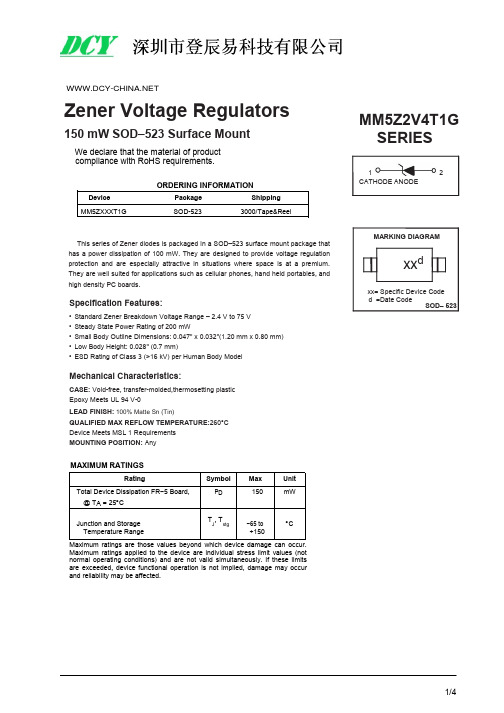
Zener Voltage Regulators150mW SOD–523Surface MountWe declare that the material of product compliance with RoHS requirements.ORDERING INFORMATIONDevice Package Shipping MM5ZXXXT1GSOD-5233000/Tape&ReelThis series of Zener diodes is packaged in a SOD–523surface mount package that has a power dissipation of 100mW.They are designed to provide voltage regulation protection and are especially attractive in situations where space is at a premium.They are well suited for applications such as cellular phones,hand held portables,and high density PC boards.Specification Features:•Standard Zener Breakdown Voltage Range –2.4V to 75V •Steady State Power Rating of 200mW•Small Body Outline Dimensions:0.047"x 0.032"(1.20mm x 0.80mm)•Low Body Height:0.028"(0.7mm)•ESD Rating of Class 3(>16kV)per Human Body ModelMechanical Characteristics:CASE:Void-free,transfer-molded,thermosetting plastic Epoxy Meets UL 94V-0LEAD FINISH:100%Matte Sn (Tin)QUALIFIED MAX REFLOW TEMPERATURE:260°C Device Meets MSL 1Requirements MOUNTING POSITION:AnyMAXIMUM RATINGSRatingSymbol Max Unit Total Device Dissipation FR−5Board,P D150mW@T A =25︒C Junction and Storage T J,Tstg−65to ︒CTemperature Range+150Maximum ratings are those values beyond which devicedamage can occur.Maximum ratings applied to the device are individual stress limit values (not normal operating conditions)and are not valid simultaneously.If these limits are exceeded,device functional operation is not implied,damage may occur and reliability may be affected.MM5Z2V4T1G SERIES12CATHODE ANODEMARKING DIAGRAMxx dxx=Specific Device Code d =Date CodeSOD–523MM5Z2V4T1G SERIES ELECTRICAL CHARACTERISTICS I(T A=25︒C unless otherwise noted,I FV F=0.9V Max.@I F=10mA for all types)Symbol ParameterVZ Reverse Zener Voltage@I ZT IZT Reverse Current VZVRVZ ZT Maximum Zener Impedance@I I R VFZT IZTIZK Reverse CurrentZZK Maximum Zener Impedance@I ZKIR Reverse Leakage Current@V RV R Reverse VoltageI F Forward Current Zener Voltage Regulator V F Forward Voltage@I FQV Z Maximum Temperature Coefficient of V ZC Max.Capacitance@V R=0and f=1MHz100(%)80DISS IP ATI ON 60 40POWER20255075100125150TEMPERATURE(︒C)Figure1.Steady State Power Derating MM5Z2V4T1G SERIESELECTRICAL CHARACTERISTICS (T A =25︒C unless otherwise noted,V F =0.9V Max.@I F =10mA for all types)Zener Voltage (Note 1)Zener Impedance Leakage CurrentQ V Z C ZZT(mV/k)@V =0V(Volts)@I@I ZT Z@II @VRZZKR@IZTf =1MHzDevice ZTZKRDevice Marking Min Nom Max mA W W mA m A Volts Min Max pF MM5Z2V4T1G 00 2.2 2.4 2.651001000 1.050 1.0−3.50450MM5Z2V7T1G 01 2.5 2.7 2.951001000 1.020 1.0−3.50450MM5Z3V0T1G 02 2.8 3.0 3.251001000 1.010 1.0−3.50450MM5Z3V3T1G 05 3.1 3.3 3.55951000 1.05 1.0−3.50450MM5Z3V6T1G 06 3.4 3.6 3.85901000 1.05 1.0−3.50450MM5Z3V9T1G 07 3.7 3.9 4.15901000 1.03 1.0−3.5−2.5450MM5Z4V3T1G 08 4.0 4.3 4.65901000 1.03 1.0−3.50450MM5Z4V7T1G 09 4.4 4.7 5.0580800 1.03 2.0−3.50.2260MM5Z5V1T1G 0A 4.8 5.1 5.4560500 1.02 2.0−2.7 1.2225MM5Z5V6T1G 0C 5.2 5.6 6.0540400 1.01 2.0−2.0 2.5200MM5Z6V2T1G 0E 5.8 6.2 6.6510100 1.03 4.00.4 3.7185MM5Z6V8T1G 0F 6.4 6.87.2515160 1.02 4.0 1.2 4.5155MM5Z7V5T1G 0G 7.07.57.9515160 1.01 5.0 2.5 5.3140MM5Z8V2T1G 0H 7.78.28.7515160 1.00.7 5.0 3.2 6.2135MM5Z9V1T1G 0K 8.59.19.6515160 1.00.27.0 3.87.0130MM5Z10VT1G 0L 9.41010.6520160 1.00.18.0 4.58.0130MM5Z11VT1G 0M 10.41111.6520160 1.00.18.0 5.49.0130MM5Z12VT1G 0N 11.41212.752580 1.00.18.0 6.010130MM5Z13VT1G 0P 12.413.2514.153080 1.00.18.07.011120MM5Z15VT1G 0T 14.31515.8530200 1.00.0510.59.213110MM5Z16VT1G 0U 15.316.217.1240200 1.00.0511.210.414105MM5Z18VT1G 0W 16.81819.1245225 1.00.0512.612.416100MM5Z20VT1G 0Z 18.82021.2255225 1.00.0514.014.41885MM5Z22VT1G 1020.82223.3255250 1.00.0515.416.42085MM5Z24VT1G 1122.824.225.6270120 1.00.0516.818.42280MM5Z27VT1G 1225.12728.9280300 1.00.0518.921.425.370MM5Z30VT1G 14283032280300 1.00.0521.024.429.470MM5Z33VT1G 18313335280300 1.00.0523.227.433.470MM5Z36VT1G 19343638290500 1.00.0525.230.437.470MM5Z39VT1G 203739412130500 1.00.0527.333.441.245MM5Z43VT1G 214043461150500 1.00.0530.137.646.640MM5Z47VT1G 1A 4447501170500 1.00.0532.942.051.840MM5Z51VT1G 1C 4851541180500 1.00.0535.746.657.240MM5Z56VT1G 1D 5256601200500 1.00.0539.252.263.840MM5Z62VT1G 1E 5862661215500 1.00.0543.458.871.635MM5Z68VT1G 1F 6468721240500 1.00.0547.665.679.835MM5Z75VT1G1G70757912555001.00.0552.573.488.6351.Zener voltage is measured with a pulse test current I Z at an ambient temperature of 25︒C.MM5Z2V4T1G SERIESSC-79/SOD-523DIMENSIONS (mm are the original dimensions)UNIT A b p c D E H E V m m0.70.350.2 1.30.9 1.70.150.50.250.11.10.71.5Note1.The marking bar indicates the cathode.OUTLINE REFERENCES EUROPEAN ISSUE DATEVERSION IECJEDECEIAJ PROJECTIONSOD523SC-7998-11-25。
MMSZ5240中文资料
1/20/99
元器件交易网
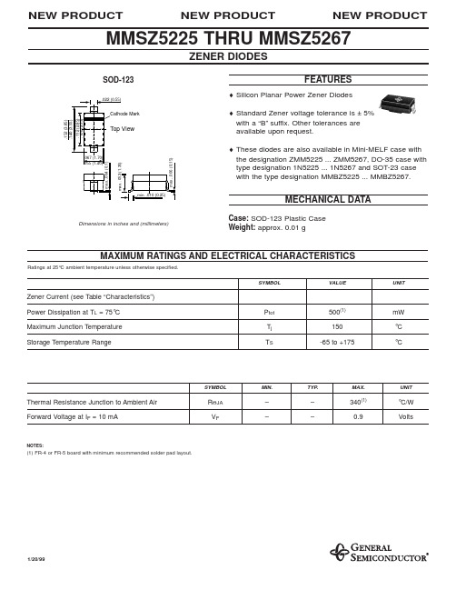
MMSZ5225 THRU MMSZ5267
ELECTRICAL CHARACTERISTICS
Ratings at 25°C ambient temperature unless otherwise specified.
Type
Marking Code
MECHANICAL DATA
Case: SOD-123 Plastic Case Weight: approx. 0.01 g
Dimensions in inches and (millimeters)
MAXIMUM RATINGS AND ELECTRICAL CHARACTERISTICS
Ratings at 25°C ambient temperature unless otherwise specified.
-0.075 -0.070 -0.065 -0.060 -0.055 ±0.030 ±0.030 +0.038 +0.038 +0.045 +0.050 +0.058 +0.062 +0.065 +0.068 +0.075 +0.076 +0.077 +0.079 +0.082 +0.082 +0.083 +0.084 +0.085 +0.086 +0.086 +0.087 +0.087 +0.089 +0.090 +0.091 +0.091 +0.092 +0.093 +0.094 +0.095 +0.095 +0.096 +0.096 +0.097 +0.097 +0.097 +0.098
MM5Z5V1中文资料

Cathode
Anode
WEITRON
元器件交易网
MM5Z2V4 Series
WE IT R ON
E L E C T R IC A L C HA R A C T E R IS T IC S (T A = 25 C unles s otherwis e noted, V F = 0.9 V Max. @ I F = 10 mA for all types )
Symbol
VZ I ZT Z ZT IR VR IF VF θV Z C R evers e C urrent
Parameter
R evers e Zener Voltage @ IZT
Maximum Zener Impedance @ I ZT R evers e Leakage C urrent @ V R R evers e Voltage F orward C urrent F orward Voltage @ I F Maximum Temperature C oefficient of V Z Max. C apacitance @ V R = 0 and f = 1 MHz
WEITRON
(TA=25 C Unless Otherwise Noted)
Symbol
PD R θJA VF Tj,TSTG
Value
100 625 0.9 -65 to+150
Unit
mW C/W V C
ELECTRICAL CHARACTERISTICS
(T A = 25 C unles s otherwis e noted, V F = 0.9 V Max. @ I F = 10 mA) I IF
Device Marking 00 01 02 05 06 07 08 09 0A 0C 0E 0F 0G 0H 0K 0L 0M 0N 0P 0T 0U 0W 0Z 10 11 12 14 18 19 20 21 1A 1C 1D 1E 1F 1G
MMSZ5230中文资料

1/20/99
元器件交易网
MMSZ5225 THRU MMSZ5267
ELECTRICAL CHARACTERISTICS
Ratings at 25°C ambient temperature unless otherwise specified.
Type
Marking Code
-0.075 -0.070 -0.065 -0.060 -0.055 ±0.030 ±0.030 +0.038 +0.038 +0.045 +0.050 +0.058 +0.062 +0.065 +0.068 +0.075 +0.076 +0.077 +0.079 +0.082 +0.082 +0.083 +0.084 +0.085 +0.086 +0.086 +0.087 +0.087 +0.089 +0.090 +0.091 +0.091 +0.092 +0.093 +0.094 +0.095 +0.095 +0.096 +0.096 +0.097 +0.097 +0.097 +0.098
1.0 1.0 1.0 1.0 1.0 2.0 2.0 3.0 3.5 4.0 5.0 6.0 6.5 6.5 7.0 8.0 8.4 9.1 9.9 10 11 12 13 14 14 15 17 18 19 21 21 23 25 27 30 33 36 39 43 46 47 52 56
NOTES: (1) The Zener Impedance is derived from the 1kHz AC voltage which results when an AC current having an RMS value equal to 10% of the Zener current (IZT or IZK) is superimposed on IZT or IZK. Zener Impedance is measured at two points to insure a sharp knee on the breakdown curve and to eliminate unstable units. (2) Measured with device junction in thermal equilibrium.
MMSZ5_稳压管

TAK CHEONG®SEMICONDUCTOR500mW SOD-123 SURFACE MOUNTFlat Lead Surface Mount Plastic Package Zener Voltage RegulatorsGreen ProductAbsolute Maximum RatingsT A = 25°C unless otherwise notedSymbol Parameter Value UnitsP D Power Dissipation500 mW T STGStorage Temperature Range -65 to +150°C T OPROperating Temperature Range-65 to +150°CThese ratings are limiting values above which the serviceability of the diode may be impaired.Specification Features:Wide Zener Voltage Range Selection, 2.4V to 75V VZ Tolerance Selection of ±5% (C Series) Flat Lead SOD-123 Plastic Package Surface Device Type Mounting RoHS Compliant Green EMCMatte Tin(Sn) Lead FinishBand Indicates CathodeElectrical CharacteristicsT A = 25°C unless otherwise noted V Z @ I ZT (Volts)Device TypeDevice MarkingMin Nom MaxI ZT (mA)Z ZT @ I ZT(Ω) Max I ZK (mA)Z ZK @ I ZK (Ω) Max I R @ V R (μA) Max V R (Volts) MMSZ2V4CW 2V4Z 2.28 2.4 2.52 5 100 1 564 45 1 MMSZ2V7CW 2V7Z 2.57 2.7 2.84 5 100 1 564 18 1 MMSZ3V0CW 3V0Z 2.85 3.0 3.15 5 100 1 564 9 1 MMSZ3V3CW 3V3Z 3.14 3.3 3.47 5 95 1 564 4.5 1 MMSZ3V6CW 3V6Z 3.42 3.6 3.78 5 90 1 564 4.5 1 MMSZ3V9CW 3V9Z 3.71 3.9 4.10 5 90 1 564 2.7 1 MMSZ4V3CW 4V3Z 4.09 4.3 4.52 5 90 1 564 2.7 1 MMSZ4V7CW 4V7Z 4.47 4.7 4.94 5 80 1 470 2.7 2 MMSZ5V1CW 5V1Z 4.85 5.1 5.36 5 60 1 451 1.8 2 MMSZ5V6CW 5V6Z 5.32 5.6 5.88 5 40 1 376 0.9 2 MMSZ6V2CW 6V2Z 5.89 6.2 6.51 5 10 1 141 2.7 4 MMSZ6V8CW 6V8Z 6.46 6.8 7.14 5 15 1 75 1.8 4 MMSZ7V5CW 7V5Z 7.11 7.5 7.86 5 15 1 75 0.9 5 MMSZ8V2CW 8V2Z 7.79 8.2 8.61 5 15 1 75 0.63 5 MMSZ9V1CW 9V1Z 8.65 9.1 9.56 5 15 1 94 0.45 6 MMSZ10VCW 10VZ 9.50 10 10.50 5 20 1 141 0.18 7 MMSZ11VCW 11VZ 10.45 11 11.55 5 20 1 141 0.09 8 MMSZ12VCW 12VZ 11.40 12 12.60 5 25 1 141 0.09 8 MMSZ13VCW 13VZ 12.35 13 13.65 5 30 1 160 0.098MMSZ15VCW 15VZ 14.25 15 15.75 5 30 1 188 0.045 10.5 MMSZ16VCW 16VZ 15.20 16 16.8054011880.045 11.2ELECTRICAL SYMBOLM M S Z 2V 4C W t h r o u g h M M S Z 75CathodeAnodeSOD-123 Flat LeadTAK CHEONGSEMICONDUCTORElectrical CharacteristicsT A = 25°C unless otherwise noted V Z @ I ZT (Volts)Device TypeDevice MarkingMin Nom MaxI ZT (mA)Z ZT @ I ZT (Ω) Max I ZK (mA) Z ZK @ I ZK (Ω) MaxI R @ V R (μA) Max V R (Volts) MMSZ18VCW 18VZ 17.10 18 18.90 5 45 1 212 0.045 12.6 MMSZ20VCW 20VZ 19.00 20 21.00 5 55 1 212 0.045 14.0 MMSZ22VCW 22VZ 20.90 22 23.10 5 55 1 235 0.045 15.4 MMSZ24VCW 24VZ 22.80 24 25.20 5 70 1 235 0.045 16.8 MMSZ27VCW 27VZ 25.65 27 28.35 5 80 0.5 282 0.045 18.9 MMSZ30VCW 30VZ 28.50 30 31.50 5 80 0.5 282 0.045 21.0 MMSZ33VCW 33VZ 31.35 33 34.65 5 80 0.5 306 0.045 23.0 MMSZ36VCW 36VZ 34.20 36 37.80 5 90 0.5 329 0.045 25.2 MMSZ39VCW 39VZ 37.05 39 40.95 5 130 0.5 329 0.045 27.3 MMSZ43VCW 43VZ 40.85 43 45.15 5 150 0.5 353 0.045 30.1 MMSZ47VCW 47VZ 44.65 47 49.35 5 170 0.5 353 0.045 33.0 MMSZ51VCW 51VZ 48.45 51 53.55 5 180 0.5 376 0.045 35.7 MMSZ56VCW 56VZ 53.20 56 58.80 5 200 0.5 400 0.045 39.2 MMSZ62VCW 62VZ 58.90 62 65.10 5 215 0.5 423 0.045 43.4 MMSZ68VCW 68VZ 64.60 68 71.40 5 240 0.5 447 0.045 47.6 MMSZ75VCW 75VZ 71.25 75 78.7552550.54700.04552.5V F Forward Voltage = 900mV Maximum @ I F = 10 mA for all typesNotes:1. The Zener Voltage (V Z ) is tested under pulse condition of 10mS.2. The device numbers listed have a standard tolerance on the nominal zener voltage of ±5%.3.For detailed information on price, availability and delivery of nominal zener voltages between the voltages shown and tighter voltage tolerances, contact your nearest Tak Cheong Electronics representative.4.The zener impedance is derived from the 60-cycle ac voltage, which results when an ac current having an rms value equal to 10% of the dc zener current (I ZT or I ZK ) is superimposed to I ZT or I ZK.TAK CHEONGSEMICONDUCTOR RATING AND CHARACTERISTIC CURVESFig.1 TYPICAL FORWARD VOLTAGE Fig.2 EFFECT OF ZENER VOLTAGE ON ZENER IMPEDANCE Fig.3 MAXIMUM NONREPETITIVE SURGE Fig.4 TYPICAL CAPACITANCEFig.5 ZENER BREAKDOWN CHARACTERISTICS Fig.6 ZENER BREAKDOWN CHARACTERISTICSTAK CHEONGSEMICONDUCTOR Fig.7 TYPICAL LEAKGE CURRENTTAK CHEONGSEMICONDUCTORFlat Lead SOD-123 Package Outline。
- 1、下载文档前请自行甄别文档内容的完整性,平台不提供额外的编辑、内容补充、找答案等附加服务。
- 2、"仅部分预览"的文档,不可在线预览部分如存在完整性等问题,可反馈申请退款(可完整预览的文档不适用该条件!)。
- 3、如文档侵犯您的权益,请联系客服反馈,我们会尽快为您处理(人工客服工作时间:9:00-18:30)。
MM5Z2V4 Series Surface Mount Zener Diodes
Features: *100mw Power Dissipation *Ideal for Surface Mountted Application *Zener Breakdown Voltage Range 2.4V to 75V *ESD Rating of Class 3(>kv)per Human Body Model Mechanical Data: *Case : SOD-523 Molded plastic *Terminals: Solderable per MIL-STD-202, Method 208 *Polarity: Cathode Indicated by Polarity Band *Marking: Marking Code (See Table on Page 3)
VZ VR IR V F I ZT
V
Zener V oltage Regulator
Device Marking
Item MM5Z2V4 Series Marking XX=Specific Device Code (See Table on page3) Equivalent Circuit Diagram
P IN 1. C A T HODE 2. A NODE
WEITRON
元器件交易网
MM5Z2V4 Series
Maximum Ratings and Electrical Characteristics
Characteristics
mA 1.0 1.0 1.0 1.0 1.0 1.0 1.0 1.0 1.0 1.0 1.0 1.0 1.0 1.0 1.0 1.0 1.0 1.0 1.0 1.0 1.0 1.0 1.0 1.0 1.0 1.0 1.0 1.0 1.0 1.0 1.0 1.0 1.0 1.0 1.0 1.0 1.0
Devic e MM5Z2V 4 MM5Z2V 7 MM5Z3V 0 MM5Z3V 3 MM5Z3V 6 MM5Z3V 9 MM5Z4V 3 MM5Z4V 7 MM5Z5V 1 MM5Z5V 6 MM5Z6V 2 MM5Z6V 8 MM5Z7V 5 MM5Z8V 2 MM5Z9V 1 MM5Z10V MM5Z11V MM5Z12V MM5Z13V MM5Z15V MM5Z16V MM5Z18V MM5Z20V MM5Z22V MM5Z24V MM5Z27V MM5Z30V MM5Z33V MM5Z36V MM5Z39V MM5Z43V MM5Z47V MM5Z51V MM5Z56V MM5Z62V MM5Z68V MM5Z75V
Ω
1000 1000 1000 1000 1000 1000 1000 800 500 200 100 160 160 160 160 160 160 80 80 80 80 80 100 100 120 300 300 300 500 500 500 500 500 500 500 500 500
SMALL SIGNAL ZENER DIODES 100m WATTS
1 2
SOD-523
SOD-523 Outline Dimensions
Unit:mm
S OD-523
Dim A B C D E J K Min 1.10 0.70 0.50 0.25 0.15 0.07 1.50 Max 1.30 0.90 0.70 0.35 0.25 0.20 1.70
WEITRON
(TA=25 C Unless Otherwise Noted)
Symbol
PD R θJA VF Tj,TSTG
Hale Waihona Puke Value100 625 0.9 -65 to+150
Unit
mW C/W V C
ELECTRICAL CHARACTERISTICS
(T A = 25 C unles s otherwis e noted, V F = 0.9 V Max. @ I F = 10 mA) I IF
Zener Voltage (Note 1) V Z (Volts ) Min 2.2 2.5 2.8 3.1 3.4 3.7 4.0 4.4 4.8 5.2 5.8 6.4 7.0 7.7 8.5 9.4 10.4 11.4 12.4 14.3 15.3 16.8 18.8 20.8 22.8 25.1 28 31 34 37 40 44 48 52 58 64 70 Nom 2.4 2.7 3.0 3.3 3.6 3.9 4.3 4.7 5.1 5.6 6.2 6.8 7.5 8.2 9.1 10 11 12 13.25 15 16.2 18 20 22 24.2 27 30 33 36 39 43 47 51 56 62 68 75 Max 2.6 2.9 3.2 3.5 3.8 4.1 4.6 5.0 5.4 6.0 6.6 7.2 7.9 8.7 9.6 10.6 11.6 12.7 14.1 15.8 17.1 19.1 21.2 23.3 25.6 28.9 32 35 38 41 46 50 54 60 66 72 79 @ I ZT mA 5 5 5 5 5 5 5 5 5 5 5 5 5 5 5 5 5 5 5 5 2 2 2 2 2 2 2 2 2 2 1 1 1 1 1 1 1 Zener Impedanc e Z ZT @ I ZT Z ZK @ I ZK L eakage C urrent IR @ VR uA 50 20 10 5 5 3 3 3 2 1 3 2 1 0.7 0.2 0.1 0.1 0.1 0.1 0.05 0.05 0.05 0.05 0.05 0.05 0.05 0.05 0.05 0.05 0.05 0.05 0.05 0.05 0.05 0.05 0.05 0.05 Volts 1.0 1.0 1.0 1.0 1.0 1.0 1.0 2.0 2.0 2.0 4.0 4.0 5.0 5.0 7.0 8.0 8.0 8.0 8.0 10.5 11.2 12.6 14.0 15.4 16.8 18.9 21.0 23.2 25.2 27.3 30.1 32.9 35.7 39.2 43.4 47.6 52.5 VZ (mV /k) @ I ZT Min -3.5 -3.5 -3.5 -3.5 -3.5 -3.5 -3.5 -3.5 -2.7 -2.0 0.4 1.2 2.5 3.2 3.8 4.5 5.4 6.0 7.0 9.2 10.4 12.4 14.4 16.4 18.4 21.4 24.4 27.4 30.4 33.4 37.6 42.0 46.6 52.2 58.8 65.6 73.4 Max 0 0 0 0 0 -2.5 0 0.2 1.2 2.5 3.7 4.5 5.3 6.2 7.0 8.0 9.0 10 11 13 14 16 18 20 22 25.3 29.4 33.4 37.4 41.2 46.6 51.8 57.2 63.8 71.6 79.8 88.6 C @ V R =0 f=1MHz pF 450 450 450 450 450 450 450 260 225 200 185 155 140 135 130 130 130 130 120 110 105 100 85 85 80 70 70 70 70 45 40 40 40 40 35 35 35
1 2
Cathode
Anode
WEITRON
元器件交易网
MM5Z2V4 Series
WE IT R ON
E L E C T R IC A L C HA R A C T E R IS T IC S (T A = 25 C unles s otherwis e noted, V F = 0.9 V Max. @ I F = 10 mA for all types )
Total Power Dissipation on FR-5 Board (1) @TA=25 C Thermal Resistance Junction to Ambient Air (1) Forward Voltage @ IF=10mA Junction and Storage Temperature Range NOTES:1.FR-4 Minimun Pad
1. Zener voltage is meas ured with a puls e tes t current I Z at an ambient temperature of 25 C .
WEITRON
Symbol
VZ I ZT Z ZT IR VR IF VF θV Z C R evers e C urrent
Parameter
R evers e Zener Voltage @ IZT
Maximum Zener Impedance @ I ZT R evers e Leakage C urrent @ V R R evers e Voltage F orward C urrent F orward Voltage @ I F Maximum Temperature C oefficient of V Z Max. C apacitance @ V R = 0 and f = 1 MHz
Device Marking 00 01 02 05 06 07 08 09 0A 0C 0E 0F 0G 0H 0K 0L 0M 0N 0P 0T 0U 0W 0Z 10 11 12 14 18 19 20 21 1A 1C 1D 1E 1F 1G
Ω
100 100 100 95 90 90 90 80 60 40 10 15 15 15 15 20 20 25 30 30 40 45 55 55 70 80 80 80 90 130 150 170 180 200 215 240 255