2354EC配套素材
2353.2354简易手册

JMA-2353/2354 简易手册先说一下多功能旋钮,以下简称“M”,以后涉及到的操作按此进行不再重复。
1)按M,出现软键菜单,转动M,选择项目。
下面4个软键对应使用。
2)再按M相当于确认键(ENTER),返回或退出用消除键(CLEAR)。
大部分的设置和操作都可用多功能(M)实现,回去就用CLEAR (消除)。
M+CLEAR是这个型号雷达的常用操作手段,M键多加操练,无需说明书可操作自如。
使用前此部分内容主要供安装人员,使用者可跳过。
1)按说明书正确安装连接显示器和天线后,确认电源为直流24V,电源插头白接正黑接负。
面板换上中文面板,显示器右侧面贴上对应的型号铭牌(JMA-2353或JMA-2354)。
2)接入GPS、罗径和AIS等信号GPS信号接入雷达GPS端(6芯)3和4罗径信号接入雷达EXTI端(8芯)3和4AIS信号接入雷达EXTI端(8芯)5和6(注意串口波特率设置)◆罗径信号如是0183信号,在调整菜单→接口装置→艏向设备→选择罗径。
◆若无罗径信号,在调整菜单→接口装置→艏向设备→选择全球定位系统。
◆按菜单键→测试→线路监视,可检查以上信号是否正常。
3)初始设置按住MENU直到代码输入窗口跳出,按M→转动M选择第1项→进入基本调整。
a)更改语言为中文(不需要改的跳过)选择第5项→更改语言为Chineseb)方位调整(调船首线)在显示航向向上(HUP)模式下调整,选择第1项方位调整→转动M调整船首线→正确后按M确认。
c)距离调整(调零海里)选择第2项距离调整→转动M调整→正确后按M确认。
d)调谐调整(调图像)量程设为48mm或以上,选择第3项→转动M使回波最佳→按M确认。
e)天线高度调整(天线离水面的距离)一定要调,涉及到海浪抑制(近程增益)的效果,选择第4项天线高度→转动M选择正确的天线高度→按M确认。
注意:调整菜单和使用功能内容较多,在明白情况下调整和使用。
简化使用,复杂菜单可先置之不用。
TLC1543
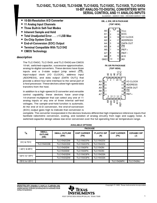
IMPORTANT NOTICETexas Instruments (TI) reserves the right to make changes to its products or to discontinue any semiconductor product or service without notice, and advises its customers to obtain the latest version of relevant information to verify, before placing orders, that the information being relied on is current.TI warrants performance of its semiconductor products and related software to the specifications applicable at the time of sale in accordance with TI’s standard warranty. Testing and other quality control techniques are utilized to the extent TI deems necessary to support this warranty. Specific testing of all parameters of each device is not necessarily performed, except those mandated by government requirements.Certain applications using semiconductor products may involve potential risks of death, personal injury, or severe property or environmental damage (“Critical Applications”).TI SEMICONDUCTOR PRODUCTS ARE NOT DESIGNED, INTENDED, AUTHORIZED, OR WARRANTED TO BE SUITABLE FOR USE IN LIFE-SUPPORT APPLICATIONS, DEVICES OR SYSTEMS OR OTHER CRITICAL APPLICATIONS.Inclusion of TI products in such applications is understood to be fully at the risk of the customer. Use of TI products in such applications requires the written approval of an appropriate TI officer. Questions concerning potential risk applications should be directed to TI through a local SC sales office.In order to minimize risks associated with the customer’s applications, adequate design and operating safeguards should be provided by the customer to minimize inherent or procedural hazards.TI assumes no liability for applications assistance, customer product design, software performance, or infringement of patents or services described herein. Nor does TI warrant or represent that any license, either express or implied, is granted under any patent right, copyright, mask work right, or other intellectual property right of TI covering or relating to any combination, machine, or process in which such semiconductor products or services might be or are used.Copyright © 1995, Texas Instruments Incorporated。
3-4素材

江西生物科技职业学院学生姓名:张晓专业班级:××××××论文名称:多媒体课件制作指导教师:××××××目录前言 (1)1. 光纤通信的发展概况及动向 (1)1.1 发展概况 (1)1.2 发展动向 (1)2. 多媒体CAI的认识 (2)2.1 超媒体结构 (2)2.2 表现力强 (2)2.3 交互性强 (2)2.4 可以进行网上传输 (3)3. 软件开发平台的介绍 (3)3.1 硬件平台介绍 (3)3.2 软件平台介绍 (3)3.2.1 软件平台概述 (3)3.2.2 多媒体软件开发工具---Authorware 5。
0 (4)4. 软件的制作过程 (5)4.1 教学设计 (5)4.2 编写脚本 (6)4.3 媒体制作 (6)4.3.1 在Authorware中搭建程序的整体框架 (6)4.3.2 软件的素材积累 (6)4.3.3 框架内容的充实和完善 (6)5. 软件制作过程中的体会 (8)结束语 (9)文档名称摘要本文简要介绍了光纤通信发展的历史及现状,较全面的向大家展现了制作 "光缆开剥与接续"多媒体课件的过程。
与此同时,还对课件制作过程中使用的工具和器材及作者的心得体会作了基本介绍,希望能给读者以启发。
关键词光纤通信软件开发制作过程开剥接续封合前言光纤通信自问世以来,通过其通信容量大、传输距离长、抗电磁干扰、保密性好、重量轻、资源丰富等优点,已经广泛应用于市内局间中继,长途通信和海底通信等公用通信网以及铁道、电力等专用通信网,同时在公用电话、广播和计算机专用网中得到应用。
并已逐渐用于用户系统。
光缆将取代过去用户系统无法实现宽频信息传输的传统线路,这样便可提供高质量的电视图像和高速数据等新业务,以满足人们广泛的生活和业务的需要。
光缆线路,是光纤通信系统组成的重要部分。
PMBT3904,215;PMBT3904,235;中文规格书,Datasheet资料

Product data sheet Supersedes data of 1999 Apr 272004 Jan 12NPN switching transistor PMBT3904FEATURES•Collector current capability I C = 200 mA •Collector-emitter voltage V CEO = 40 V.APPLICATIONS•General switching and amplification.DESCRIPTIONNPN switching transistor in a SOT23 plastic package. PNP complement: PMBT3906.MARKINGNote1.* = p : Made in Hong Kong.* = t : Made in Malaysia.* = W : Made in China.QUICK REFERENCE DATA PINNINGTYPE NUMBER MARKING CODE(1) PMBT3904*1ASYMBOL PARAMETER MAX.UNIT V CEO collector-emitter voltage40VI C collector current (DC)200mAPIN DESCRIPTION1base2emitter3collectorORDERING INFORMATIONTYPE NUMBERPACKAGENAME DESCRIPTION VERSIONPMBT3904−plastic surface mounted package; 3 leads SOT23NPN switching transistorPMBT3904LIMITING VALUESIn accordance with the Absolute Maximum Rating System (IEC 60134).Note1.Transistor mounted on an FR4 printed-circuit board.THERMAL CHARACTERISTICS Note1.Transistor mounted on an FR4 printed-circuit board.CHARACTERISTICST amb = 25 °C unless otherwise specified.SYMBOL PARAMETERCONDITIONS MIN.MAX.UNITV CBO collector-base voltage open emitter −60V V CEO collector-emitter voltage open base −40V V EBO emitter-base voltage open collector−6VI C collector current (DC)−200mA I CM peak collector current −200mA I BM peak base current −100mA P tot total power dissipation T amb ≤ 25 °C; note 1−250mW T stg storage temperature −65+150°C T j junction temperature−150°C T amb operating ambient temperature−65+150°CSYMBOL PARAMETERCONDITIONS VALUE UNIT R th(j-a)thermal resistance from junction to ambientnote 1500K/WSYMBOL PARAMETERCONDITIONSMIN.MAX.UNIT I CBO collector cut-off current I E = 0; V CB = 30 V −50nA I EBO emitter cut-off current I C = 0; V EB = 6 V−50nAh FEDC current gainV CE = 1 V; see Fig.2; note 1I C = 0.1 mA 60−I C = 1 mA 80−I C = 10 mA 100300I C = 50 mA 60−I C = 100 mA30−V CEsat collector-emitter saturation voltageI C = 10 mA; I B = 1 mA −200mV I C = 50 mA; I B = 5 mA −300mV V BEsat base-emitter saturation voltage I C = 10 mA; I B = 1 mA 650850mV I C = 50 mA; I B = 5 mA−950mV C c collector capacitance I E = I e = 0; V CB = 5 V; f = 1 MHz −4pF C eemitter capacitanceI C = I c = 0; V BE = 500 mV; f = 1 MHz−8pFNPN switching transistor PMBT3904Note1.Pulse test: t p ≤ 300 µs; δ ≤ 0.02.f T transition frequency I C = 10 mA; V CE = 20 V; f = 100 MHz300−MHz Fnoise figureI C = 100 µA; V CE = 5 V; R S = 1 k Ω; f = 10 Hz to 15.7 kHz −5dBSwitching times (between 10% and 90% levels); see Fig.3t d delay time I Con = 10 mA; I Bon = 1 mA; I Boff = −1 mA−35ns t r rise time −35ns t s storage time −200ns t f fall time−50nsSYMBOL PARAMETERCONDITIONSMIN.MAX.UNITNPN switching transistor PMBT3904NPN switching transistor PMBT3904NPN switching transistor PMBT3904 PACKAGE OUTLINENPN switching transistorPMBT3904DATA SHEET STATUSNotes1.Please consult the most recently issued document before initiating or completing a design.2.The product status of device(s) described in this document may have changed since this document was publishedand may differ in case of multiple devices. The latest product status information is available on the Internet at URL . DOCUMENT STATUS (1)PRODUCT STATUS (2)DEFINITIONObjective data sheet Development This document contains data from the objective specification for product development.Preliminary data sheet Qualification This document contains data from the preliminary specification. Product data sheet ProductionThis document contains the product specification.DISCLAIMERSGeneral ⎯ Information in this document is believed to be accurate and reliable. However, NXP Semiconductors does not give any representations or warranties,expressed or implied, as to the accuracy or completeness of such information and shall have no liability for the consequences of use of such information.Right to make changes ⎯ NXP Semiconductors reserves the right to make changes to informationpublished in this document, including without limitation specifications and product descriptions, at any time and without notice. This document supersedes and replaces all information supplied prior to the publication hereof.Suitability for use ⎯ NXP Semiconductors products are not designed, authorized or warranted to be suitable for use in medical, military, aircraft, space or life support equipment, nor in applications where failure or malfunction of an NXP Semiconductors product can reasonably be expected to result in personal injury, death or severe property or environmental damage. NXP Semiconductors accepts no liability for inclusion and/or use of NXP Semiconductors products in such equipment orapplications and therefore such inclusion and/or use is at the customer’s own risk.Applications ⎯ Applications that are described herein for any of these products are for illustrative purposes only. NXP Semiconductors makes no representation or warranty that such applications will be suitable for the specified use without further testing or modification.Limiting values ⎯ Stress above one or more limiting values (as defined in the Absolute Maximum Ratings System of IEC 60134) may cause permanent damage to the device. Limiting values are stress ratings only and operation of the device at these or any other conditions above those given in the Characteristics sections of this document is not implied. Exposure to limiting values for extended periods may affect device reliability.Terms and conditions of sale ⎯ NXP Semiconductors products are sold subject to the general terms and conditions of commercial sale, as published at /profile/terms, including those pertaining to warranty, intellectual property rightsinfringement and limitation of liability, unless explicitly otherwise agreed to in writing by NXP Semiconductors. In case of any inconsistency or conflict between information in this document and such terms and conditions, the latter will prevail.No offer to sell or license ⎯ Nothing in this document may be interpreted or construed as an offer to sell products that is open for acceptance or the grant, conveyance or implication of any license under any copyrights, patents or other industrial or intellectual property rights.Export control ⎯ This document as well as the item(s) described herein may be subject to export controlregulations. Export might require a prior authorization from national authorities.Quick reference data ⎯ The Quick reference data is an extract of the product data given in the Limiting values and Characteristics sections of this document, and as such is not complete, exhaustive or legally binding.NXP SemiconductorsCustomer notificationThis data sheet was changed to reflect the new company name NXP Semiconductors. No changes were made to the content, except for the legal definitions and disclaimers.Contact informationFor additional information please visit: For sales offices addresses send e-mail to: salesaddresses@© NXP B.V. 2009All rights are reserved. Reproduction in whole or in part is prohibited without the prior written consent of the copyright owner.The information presented in this document does not form part of any quotation or contract, is believed to be accurate and reliable and may be changed without notice. No liability will be accepted by the publisher for any consequence of its use. Publication thereof does not convey nor imply any license under patent- or other industrial or intellectual property rights.Printed in The Netherlands R75/04/pp9 Date of release: 2004 Jan 12Document order number: 9397 750 12461分销商库存信息:NXPPMBT3904,215PMBT3904,235。
OB2354_DataSheet_Raiser_080124

to turn off
n VTH_OC
Internal Current Limiting
FB=3.3V
0.72 0.77 0.82 V
O Threshold Voltage
Oscillator
controller with a high voltage power MOSFET. It
Current
is optimized for high performance, low standby power, and cost effective off-line flyback converter applications in sub 20W range. OB2354 offers complete protection coverage with
RθJA (℃/W)
Pin Configuration
DIP8
75
The OB2354 is offered in DIP8 package as shown
Note: Drain Pin Connected to 100mm2 PCB copper clad.
below.
tial to Raiser Ordering Information
270
ns
rigblanking time
ZSENSE_IN
Input Impedance
40
Kohm
-B TD_OC
Over Current
From Over Current Occurs
120
nSec
Detection and
till the Gatedrive output start
Control Delay
医学英语课程思政教学素材资源库建设

0引言2020《》(〔2020〕3),,。
ESP()。
,[1]。
,,,[2]。
,,。
,,,、,,“”,。
,,,。
1医学英语课程思政教学素材资源库建设原则1.1准确性原则,[3]。
,“”“”“”,,。
1.2实用性原则,,,。
、、,。
医学英语课程思政教学素材资源库建设熊璟(南昌医学院,江西南昌330004)【摘要】“新文科”大背景下,医学院校开设的医学英语课程承载着重要的育人功能。
针对当前医学英语课程中思政教学素材资源匮乏的问题,文章探讨了医学英语课程思政教学素材资源库的建设,阐述了医学英语课程思政教学素材资源库建设中应遵循“准确性”“实用性”及“系统性”三大原则,尝试构建了以“理想信念”“医师职业精神”及“医学生个人发展”为一级元素指标的医学英语课程思政元素结构体系,并指出了医学英语课程思政教学素材资源库建设包含的具体内容。
【关键词】医学英语;课程思政;教学素材资源库中图分类号:R-4;G641;H319.3文献标识码:A DOI:10.19694/ki.issn2095-2457.2022.18.28※基金项目:教育部高教司2021第二批产学合作协同育人项目(202102093012)。
作者简介:璟熊,讲师,硕士,研究方向为英语教学。
97Science&Technology Vision科技视界1.3系统性原则,。
,,、、。
2医学英语课程思政元素结构体系构建、、,。
,,。
,,“”、“”“”(1)。
3医学英语课程思政教学素材资源库建设内容,、、。
A A1、。
A2,。
,、、A3、B B1,、B2,,B3,,。
,B4“”“”,B5。
“”,,, B6。
、、。
,B7,B8。
C C1,, C2。
,、,C3,,,。
C4,表1医学英语课程思政元素结构体系98Science&Technology Vision 科技视界、、。
3.1医学英语思政课件库,,、,,。
( ),,、,,。
3.2医学英语思政图片视频库。
e5对照 材料牌号.性能表.硬度与强度近似换算

18CrMo4
15XM 20XM 30XM 35XM 38XM 12XMф
15CrMo5 20CrMo4
34CrMo4 42CrMo4
34CrMo4 42CrMo4
35CrMoV 35XMф 5 13CrMoV 12X1Mф 4· 2 24CrMoV 25X2Mф A 5· 5 25X2M1ф A 21CrVMo 20X3MBф W12 41CrA1M 41CrA1Mo74 38XM1ф A o7 20Xф 21CrV4 40Xф A 42CrV6 51CrV4 50Xф A 50CrV4 15Xг 16MnCr5 20MnCr5 20Xг 20MnCr5 40Xг 20Xг с 25Xг с 30Xг с 30Xг с A 35Xг с A 25Xг M 20CrMo5 38Xг M 18Xг T 30MnCrTi 30Xг T 4 20XH 20NiCr6 40XH 40NiCr6 45XH 45NiCr6 50XH 12XH2 14NiCr10 15CrNi13 12XH3A 14NiCr14 20XH3A 22NiCr14 30XH3A 31NiCr14 37XH3 35NiCr18
20Cr4 34Cr4 41Cr
15X 15XA 20X 30X 35X 40X 45X 50X 38XC 12XM
15Cr3 20Cr4 28Cr4 34Cr4 41Cr4
12CrMo44
合金结构钢 合金结构钢 合金结构钢 合金结构钢 合金结构钢 合金结构钢 合金结构钢 合金结构钢 合金结构钢 合金结构钢 合金结构钢 合金结构钢 合金结构钢 合金结构钢 合金结构钢 合金结构钢 合金结构钢 合金结构钢 合金结构钢 合金结构钢 合金结构钢 合金结构钢 合金结构钢 合金结构钢 合金结构钢 合金结构钢 合金结构钢 合金结构钢 合金结构钢 合金结构钢 合金结构钢 合金结构钢 合金结构钢 合金结构钢 合金结构钢 合金结构钢 合金结构钢
2354中文资料

● Slot technology, Lizt wire recommended for proximity and skin effects reduction
● Mains insulation according to IEC60065 and IEC60950 safety standards
元器件交易网
Consumer Products
CONSUMER PRODUCTS
Pulse offers a complete range of Switch-Mode Transformers in various technologies (slot, layer and triple insulation wire) used for power supplies in television, set-top boxes, satellite receivers, DVD players, telephone chargers, and white goods. Pulse also offers a new range of specific magnetics for LCD TV power supplies and inverters to meet the growing, worldwide demand for flat-screen televisions. These innovative, components are manufactured in state-of-the-art, modern facilities. Switch-Mode Transformers, as well as new LCD components are produced in one of four different factories in China, depending on the technology. The products mentioned in this section serve as an overview of Pulse’s Consumer magnetics product line. For more information about Consumer products, contact Pulse Consumer Division Applications Engineering via e-mail at consumer@.
- 1、下载文档前请自行甄别文档内容的完整性,平台不提供额外的编辑、内容补充、找答案等附加服务。
- 2、"仅部分预览"的文档,不可在线预览部分如存在完整性等问题,可反馈申请退款(可完整预览的文档不适用该条件!)。
- 3、如文档侵犯您的权益,请联系客服反馈,我们会尽快为您处理(人工客服工作时间:9:00-18:30)。
编号:
作者姓名
所在单位
论文名称
待发表刊物名称
论文所涉及科研
项目名称
本人承诺:论文内容不涉及国家秘密和企事业秘密,否则,由此带来法律责任由作者本人和导师负责!
作者签字:导师签字:
年 月日年 月日
所在学院
意见
负责人签章:年 月 日
研究生院
意见
负责人签章:年 月日
科技处
意见
负责人签章:年 月 日
保密办公室
意见
负责人签章:年 月 日
保密委员会审批意见
负责人签章:年 月 日
备注:1、此表由保密办公室统一编号、备案
2、此表一式二份,论文提交人和校保密办公室各一份。