THX203H Datasheet_REV.G(翻译件终稿)
AMP02FSZ,AMP02FPZ,AMP02EPZ,AMP02FSZ-RL,AMP02FS-REEL,AMP02FS,AMP02FP,AMP02EP, 规格书,Datasheet 资料

Due to the AMP02’s design, its bandwidth remains very high over a wide range of gain. Slew rate is over 4 V/µs, making the AMP02 ideal for fast data acquisition systems. A reference pin is provided to allow the output to be referenced to an external dc level. This pin may be used for offset correction or level shifting as required. In the 8-lead package, sense is internally connected to the output. For an instrumentation amplifier with the highest precision, consult the AMP01 data sheet.
NC = NO CONNECT
V+
+IN RG –IN
3 – 1 6 5 4 REFERENCE OUT
G=
V– VOUT 50k⍀ = (+IN) – (–IN) RG
(
)
+1
FOR SOL CONNECT SENSE TO OUTPUT
Figure 1. Basic Circuit Connections
One Technology Way, P.O. Box 9106, Norwood, MA 02062-9106, U.S.A. Tel: 781/329-4700 Fax: 781/326-8703 © Analog Devices, Inc., 2002. All rights reserved.
WT32-ETH01 Wi-Fi 模组数据手册说明书

WT32-ETH01DATASHEETVersion1.123October,2019Disclaimer and Copyright NoticeInformation in this paper,including URL references,is subject to change without prior notice.This document is provided“as is”with no warranties whatsoever,including any warranty of merchantability, non-infringement,fitness for any particular purpose,or any warranty otherwise arising out of any proposal, specification or sample.All liability,including liability for infringement of any patent rights,relating to use of information in this document is disclaimed.No licenses,either express or implied,by estoppel or otherwise,to any intellectual property rights are granted herein.The Wi-Fi Alliance Member logo is a trademark of the Wi-Fi Alliance.All trade names,trademarks and registered trademarks mentioned in this document are property of their respective owners,and are hereby acknowledged.Revision HistoryContentsWT32-ETH01 (1)1.Overview (6)2.Features (6)3.Hardware Specifications (8)3.1System Block Diagram (8)3.2Product Images (8)3.3Pin Descriptions (9)3.4Power Supply Characteristics (10)3.4.1Supply Voltage (10)3.4.2Power Supply Modes (10)4.Instructions (11)4.1Power-on Instruction (11)4.2Indicator Instruction (11)4.3Usage Instruction (11)4.4Network Port Indicator Instruction (11)5.Interface Descriptions (12)6.Product Functions (12)6.1Default parameters (12)6.2Basic Functions (13)6.2.1Set IP/Subnet Mask/Gateway (13)6.2.2Restore Factory Settings (13)6.2.3Firmware upgrades (14)6.2.4AT Command Function Settings (14)6.2.5Data Transmission Function (14)6.3Socket Function (14)6.3.1TCP Client (14)6.3.2TCP Server (15)6.3.3UDP Client (15)6.3.4UDP Server (15)6.4Serial Port Function (15)6.4.1At Command Settings (15)6.5Bluetooth Function (15)6.5.1Bluetooth Data Transmission (15)6.6Wifi Function (16)6.6.1Internet Access (16)6.7Cable Network Access Function (16)6.7.1Internet Access (16)1.OverviewWT32-ETH01is an embedded serial port to Ethernet module based on ESP32series launched by Wireless-Tag Technology Co.Limited.Integrating an optimized TCP/IP protocol stack,it makes it easy for users to accomplish the network access of embedded devices and greatly reduces the development time cost.Moreover,the module is designed to be compatible with half pads and through-hole connectors.As the board width of it is the generic width,the module can be directly welded to boards,or connectors,or even breadboards,which is convenient for users to apply in different scenes.Esp32series IC is the SOC integrated with2.4GHz Wi-Fi and Bluetooth dual modes,with ultra-high RF performance,stability,versatility,reliability,and ultra-low power consumption.2.FeaturesTable1:Product specificationsCategory Items Product specificationsWi-Fi RF certifications FCC/CE/RoHSProtocols802.11b/g/n/e/i(802.11n,Up to150Mbps)A-MPDU and A-MSDU aggregation,0.4_s guardinterval supportFrequency range 2.4~2.5GHzBluetooth Protocols Bluetooth v4.2BR/EDR and BLE standards Radio NZIF receiver with-97dBm sensitivityHardware Network portspecificationsRJ45,10/100Mbps,Cross-direct connection adaptive Serial baud rate80~5000000On-board flash32MbitOperatingvoltage5V or3.3VOperatingcurrentAverage:80mASupply current Minimum:500mAOperatingtemperature-40°C~+85°CAmbienttemperatureNormal temperaturePackaging Half pad/Through-hole connector(Optional)SoftwareWi-Fi mode Station/softAP/SoftAP+station/P2PWi-Fi securitymechanismsWPA/WPA2/WPA2-Enterprise/WPS Encryption types AES/RSA/ECC/SHAFirmwareupdateRemote OTA upgrade via network SoftwaredevelopmentSDK used for further development NetworkingprotocolIPv4、TCP/UDPIP accessmethodsStatic IP、DHCP(Default)Transparenttransmission modesTCP Server/TCP Client/UDP Server/UDP Client UserconfigurationsAT+commands set3.Hardware Specifications3.1System Block DiagramFigure1:System Block Diagram 3.2Product ImagesFigure2:Product Images3.3Pin DescriptionsTable1:Debugging/Burning InterfacesPin Name Description1EN1Reserved debugging/burning interface;Active-high enable2GND Reserved debugging/burning interface;GND33V3Reserved debugging/burning interface;3V34TXD Reserved debugging/burning interface;IO1,TXD05RXD Reserved debugging/burning interface;IO3,RXD06IO0Reserved debugging/burning interface;IO0Table2:IO DescriptionsPin Name Description1EN1Active-high enable2CFG IO32,CFG3485_EN IO33,RS485Enable pin4RXD IO5,RXD25TXD IO17,TXD26GND GND73V323V3Power supply8GND GND95V25V Power supply10LINK Network connection indicator pin11GND GND12IO393IO39,Input only13IO363IO36,Input only14IO15IO1515I014IO1416IO12IO1217IO35IO35,Input only18IO4IO419IO2IO220GND GNDNote1:The module enables high level by default.Note2:Power supply makes a binary choice between3V3and5V.Note3:IO39,IO35and IO36only support input.3.4Power Supply Characteristics3.4.1Supply VoltageYou can make a binary choice between3V3and5V for power supply voltage of the module.3.4.2Power Supply ModesUsers can choose from the following modes flexibly according to their needs:1)Through hole(Welding pins):Power supply with Dupont line connection;●Power supply with breadboard connection;2)Half pad(Directly welded to the board):Power supply of user board.4.Instructions4.1Power-on InstructionIf the Dupont line connection is used:Find the3V3or5V power input port,and connect the corresponding voltage to it;when LED1indicator lights up,it indicates that power is on.4.2Indicator Instruction●LED1:Power light,when the power supply is normal,the indicator light is on;●LED3:Serial port indicator,RXD2(IO5)When there is data flow,the indicator light is on;●LED4:Serial port indicator,TXD2(IO17)When there is data flow,the indicator light is on;4.3Usage InstructionUsers can choose from three ways of use according to their needs:1)Through hole(Welding pins):Dupont line connection;2)Through hole(Welding pins):breadboard connection;3)Half pad:Users can directly weld the module on their own board.4.4Network Port Indicator InstructionTable3:Network Port Indicator DescriptionsNetwork PortIndicatorFunction DescriptionGreen Indicator Connection statusindicationwhen properly connected to the network,the green light is on.Yellow Indicator Data indication The indicator flashes when the module receives or sends data, including receiving network broadcast package.5.Interface Descriptions6.Product Functions6.1Default parameters ItemsDescriptions Port Baud Rate115200Serial port parametersNone/8/1Transparent Transmission Channel Serial to Ethernet transparenttransmission channel6.2Basic Functions6.2.1Set IP/Subnet Mask/Gateway1.IP address is the identity representation of the module in the LAN,which is unique in the LAN,so it can not be repeated with other devices in the same LAN.There are two ways to obtain the IP address of the module:static IP and DHCP/dynamic IP.a.Static IPStatic IP needs to be set manually by the user.In the process of setting,attention should be paid to write IP, subnet mask and gateway at the same time.Static IP is suitable for scenarios where IP and devices need to be counted and correspond to each other.You should pay attention to the correspondence of IP address,subnet mask and gateway when setting.To use static IP,you need to set each module and ensure that the IP address is not repeated with other network devices in the LAN.b.DHCP/Dynamic IPThe main function of DHCP/Dynamic IP is to dynamically obtain IP address,gateway address,DNS server address and other information from the gateway host,so as to avoid the tedious steps of setting IP address.It is applicable to scenarios where there is no requirement for IP,and it is not required to have a one-to-one correspondence between IP and module.Note:The module cannot be set to DHCP when directly connected to the computer.Generally,the computer does not have the ability to assign IP addresses.If the module is set as DHCP directly connected to the computer,it will cause the module to be in the state of waiting for IP address allocation all the time,which will cause the module to fail to perform normal transmission.The module default static IP:192.168.0.72.The subnet mask is mainly used to determine the network number and host number of the IP address,indicate the number of subnets,and determine whether the module is in the subnet.The subnet mask must be set properly.The commonly used class C subnet mask is255.255.255.0.The network number is the first24bits,the host number is the last8bits,and the number of subnets is255.If the module IP is within the range of255,it is considered that the module IP is in the subnet.3.Gateway refers to the network number of the current IP address of the module.If the module connects to the external network by accessing devices such as routers,the gateway is the IP address of the router.If the setting is wrong,the external network cannot be connected correctly.If you do not connect to devices such as routers, you do not need to set it.It’s OK by default.6.2.2Restore Factory Settings1.Restore factory settings by AT command:restore factory settings via AT+RESTORE.2.Restore factory settings by hardware:CFG to ground,restart the module.6.2.3Firmware upgradesOTA remote upgrade is the way for modules to upgrade firmware,through which more application functions can be obtained.a.Firmware upgrade can be connected to the network through wired network or wifi.b.Operate GPIO2to ground,restart the module,and enter OTA upgrade mode.c.After the upgrade is completed,disconnect GPIO2from the ground,restart the module,and it enters the normal working mode.OTA firmware upgrade instructions:when the firmware is being downloaded,the serial port TXD indicator flashes quickly;when the download is being upgraded,the serial port TXD indicator is always on;when the upgrade is successful,the serial port TXD and RXD indicators are always on;when the upgrade fails,the serial port TXD indicator flashes slowly.6.2.4AT Command Function SettingsUsers can set functions of the module by inputting AT commands through serial ports.Refer to the ESP32AT instruction set for details.6.2.5Data Transmission FunctionThe module has four data transmission ports:Serial port,Wifi,Ethernet and Bluetooth.Users can use AT commands to combine the four data ports in pairs for data transmission.Use AT+PASSCHANNEL command to set/query the module's transparent transmission channel.After the setting is complete,the module needs to be restarted to take effect.6.3Socket FunctionThe Socket working mode of the module is divided into four types:TCP Client,TCP Server,UDP Client,and UDP Server,which can be set by AT command.For AT command operation,please refer to esp32wired module AT command routine v1.2.6.3.1TCP Client1.TCP Client provides client connection for TCP network services.It initiates connection request and establish connection to the server to realize the interaction between serial port data and server data.According to the relevant provisions of TCP protocol,TCP client has the difference between connection and disconnection,so as to ensure the reliable exchange of ually used for data interaction between devices and servers,it is the most common way of networking communication.2.When the module connects TCP server as a TCP client,it needs to pay attention to the parameters such as the target IP/domain name and the target port number.Target IP can be of a local device in the same LAN.It canalso be an IP address from a different LAN or an IP address across the public network.If connecting to a server across the public network,the server is required to have a public IP.6.3.2TCP ServerIt is usually used for communication with TCP client in LAN.It is suitable for the scenario where there is no server in the LAN and there are multiple computers or mobile phones requesting data from the server.The same as TCP Client,TCP server has the difference between connection and disconnection to ensure reliable exchange of data.6.3.3UDP ClientUDP Client is a connectionless transport protocol,providing transaction-oriented simple and unreliable information transmission services.There is no connection establishment or disconnection,and data can be sent to each other only by specifying IP and port.It is usually used in data transmission scenarios where there is no requirement for the packet loss rate,the data packets are small and the transmission frequency is relatively fast, and the data is transferred to the specified IP.6.3.4UDP ServerUDP Server means that the source IP address is not verified on the basis of ordinary UDP.After receiving a UDP packet,the destination IP is changed to the data source IP and port number.When sending data,send it to the IP and port number of the most recent communicationThis mode is usually used in data transmission scenarios where multiple network devices need to communicate with the module and do not want to use TCP due to the high speed and frequency.6.4Serial Port Function6.4.1At Command SettingsUsers can input AT commands through serial ports to set functions for a module.6.4.2Transmitting Serial DataThe user makes the module enter the data transmission mode through AT command.The module can directly transfer serial port data to the corresponding data transmission end(wifi,Ethernet or Bluetooth)through the set passthrough channel.6.5Bluetooth Function6.5.1Bluetooth Data TransmissionThrough the existing Bluetooth function of the module,the module can obtain Bluetooth data,and through the set pass-through channel,the Bluetooth data can be directly transferred to the corresponding data transmission end(wifi,Ethernet or serial port).6.6Wifi Function6.6.1Internet AccessThe module wifi is connected to the Internet or LAN through a router.The user configures the socket function through the AT command.The module can establish a TCP/UDP connection and then access the user's designated server.6.7Cable Network Access FunctionStable network connection can be obtained through wired network to ensure stable network data acquisition.6.7.1Internet AccessThe module is connected to the Internet or LAN through a wired network.The user configures the socket function through the AT command.The module can establish a TCP/UDP connection and then access the user's designated server.。
0034.3114,0034.3124,0034.3119,0034.3123,0034.3127,0034.3117,0034.3118,0034.3120规格书,Datasheet 资料

Melting I²t 10.0 Intyp.
[A²s]
0.0012
0.0019
l
0.0027 l
l
0.0363 l
l
l
0.0401 l
l
l
0.057 l
l
l
0.107 l
l
l
0.064 l
l
l
0.23 l
l
l
0.256 l
l
l
0.238 l
l
l
0.544 l
l
l
0.768 l
l
l
3l
l
l
4.35 l
Voltage Drop 1.0 In max. [mV]
Voltage Drop 1.0 In typ. [mV]
Power Dissipation 1.5 In max. [mW]
Power Dissipation 1.5 In
typ. [mW]
0.02
250 1)
0.032
250 1)
0.04
Fuses
芯天下--/
Non resettable fuses
Time-Current-Curves
100000 10000 1000 100 10 1 0.1 0.01 0.001 1
Multiple of Rated Current In
0.02–0.1 A 0.125–20 A
Standards - IEC 60127-2/3 - UL 248-14 - CSA C22.2 no. 248.14
Approvals - VDE Certificate Number: 40016601 - UL File Number: E41599
英飞凌 FF225R65T3E3 XHP 3 模块 数据表
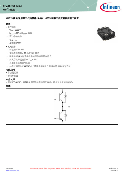
XHP ™3 模块 采用第三代沟槽栅/场终止IGBT3和第三代发射极控制二极管特性•电气特性-V CES = 6500 V-I C nom = 225 A / I CRM = 450 A -高动态稳定性-低 V CEsat -沟槽栅IGBT3•机械特性-封装的 CTI > 600-加强绝缘封装,10.4kV 交流 60 秒-碳化硅铝 (AlSiC) 基板提供更高的温度循环能力-扩大存储温度范围至 T stg = -55°C -高爬电距离和电气间隙-外壳材料符合EN45545-2 “铁路车辆防火”标准中的 R23 (HL3) 等级可选应用•牵引变流器•中压变流器产品认证•根据 IEC 60747、60749 和 60068标准的相关测试,符合工业应用的要求。
描述FF225R65T3E3XHP ™3 模块内容描述 . . . . . . . . . . . . . . . . . . . . . . . . . . . . . . . . . . . . . . . . . . . . . . . . . . . . . . . . . . . . . . . . . . . . . . . . . . . . . . . . . . . . . . . . .1特性 . . . . . . . . . . . . . . . . . . . . . . . . . . . . . . . . . . . . . . . . . . . . . . . . . . . . . . . . . . . . . . . . . . . . . . . . . . . . . . . . . . . . . . . . .1可选应用 . . . . . . . . . . . . . . . . . . . . . . . . . . . . . . . . . . . . . . . . . . . . . . . . . . . . . . . . . . . . . . . . . . . . . . . . . . . . . . . . . . . .1产品认证 . . . . . . . . . . . . . . . . . . . . . . . . . . . . . . . . . . . . . . . . . . . . . . . . . . . . . . . . . . . . . . . . . . . . . . . . . . . . . . . . . . . .1内容 . . . . . . . . . . . . . . . . . . . . . . . . . . . . . . . . . . . . . . . . . . . . . . . . . . . . . . . . . . . . . . . . . . . . . . . . . . . . . . . . . . . . . . . . .2 1封装 . . . . . . . . . . . . . . . . . . . . . . . . . . . . . . . . . . . . . . . . . . . . . . . . . . . . . . . . . . . . . . . . . . . . . . . . . . . . . . . . . . . . . . . . .3 2IGBT, 逆变器 . . . . . . . . . . . . . . . . . . . . . . . . . . . . . . . . . . . . . . . . . . . . . . . . . . . . . . . . . . . . . . . . . . . . . . . . . . . . . . . . .3 3二极管,逆变器 . . . . . . . . . . . . . . . . . . . . . . . . . . . . . . . . . . . . . . . . . . . . . . . . . . . . . . . . . . . . . . . . . . . . . . . . . . . . . . .5 4特征参数图表 . . . . . . . . . . . . . . . . . . . . . . . . . . . . . . . . . . . . . . . . . . . . . . . . . . . . . . . . . . . . . . . . . . . . . . . . . . . . . . . .6 5电路拓扑图 . . . . . . . . . . . . . . . . . . . . . . . . . . . . . . . . . . . . . . . . . . . . . . . . . . . . . . . . . . . . . . . . . . . . . . . . . . . . . . . . .10 6封装尺寸 . . . . . . . . . . . . . . . . . . . . . . . . . . . . . . . . . . . . . . . . . . . . . . . . . . . . . . . . . . . . . . . . . . . . . . . . . . . . . . . . . . .11 7模块标签代码 . . . . . . . . . . . . . . . . . . . . . . . . . . . . . . . . . . . . . . . . . . . . . . . . . . . . . . . . . . . . . . . . . . . . . . . . . . . . . . .12修订历史 . . . . . . . . . . . . . . . . . . . . . . . . . . . . . . . . . . . . . . . . . . . . . . . . . . . . . . . . . . . . . . . . . . . . . . . . . . . . . . . . . . .13免责声明 . . . . . . . . . . . . . . . . . . . . . . . . . . . . . . . . . . . . . . . . . . . . . . . . . . . . . . . . . . . . . . . . . . . . . . . . . . . . . . . . . . .141封装表 1绝缘参数特征参数代号标注或测试条件数值单位绝缘测试电压V ISOL RMS, f = 50 Hz, t = 60 s10.4kV 局部放电熄弧电压V isol RMS, f = 50 Hz, Q PD typ. 10 pC 5.1kV DC 稳定性V CE(D)T vj=25°C, 100 Fit3800V 模块基板材料AlSiC爬电距离d Creep端子至散热器53.0mm 爬电距离d Creep端子至端子53.0mm 电气间隙d Clear端子至散热器36.0mm 电气间隙d Clear端子至端子26.0mm 相对电痕指数CTI > 600表 2特征值特征参数代号标注或测试条件数值单位最小值典型值最大值杂散电感,模块L sCE25nH 模块引线电阻,端子-芯片R AA'+CC'T C=25°C, 每个开关0.33mΩ模块引线电阻,端子-芯片R CC'+EE'T C=25°C, 每个开关0.42mΩ储存温度T stg-55125°C 模块安装的安装扭距M根据相应的应用手册进行安装M6, 螺丝 4.25 5.75Nm端子安装扭矩M根据相应的应用手册进行安装M3, 螺丝0.9 1.1Nm M8, 螺丝810重量G700g 2IGBT, 逆变器表 3最大标定值特征参数代号标注或测试条件数值单位集电极-发射极电压V CES T vj = -50 °C5900VT vj = 125 °C6500连续集电极直流电流I CDC T vj max = 125 °C T C = 80 °C225A 集电极重复峰值电流I CRM t p受限于 T vj op450A 栅极-发射极峰值电压V GES±20V表 4特征值特征参数代号标注或测试条件数值单位最小值典型值最大值集电极-发射极饱和电压V CE sat I C = 225 A, V GE = 15 V T vj = 25 °C 3.00 3.40VT vj = 125 °C 3.70 4.20栅极阈值电压V GEth I C = 33 mA, V CE = V GE, T vj = 25 °C 5.406 6.60V 栅极电荷Q G V GE = ±15 V, V CE = 3600 V10.5µC 内部栅极电阻R Gint T vj = 25 °C0.67Ω输入电容C ies f = 100 kHz, T vj = 25 °C, V CE = 25 V, V GE = 0 V65.6nF 反向传输电容C res f = 100 kHz, T vj = 25 °C, V CE = 25 V, V GE = 0 V1nF 集电极-发射极截止电流I CES V CE = 6500 V, V GE = 0 V T vj = 25 °C5mA 栅极-发射极漏电流I GES V CE = 0 V, V GE = 20 V, T vj = 25 °C400nA开通延迟时间(感性负载)t don I C = 225 A, V CE = 3600 V,V GE = ±15 V, R Gon = 4.7 ΩT vj = 25 °C0.240µs T vj = 125 °C0.240上升时间(感性负载)t r I C = 225 A, V CE = 3600 V,V GE = ±15 V, R Gon = 4.7 ΩT vj = 25 °C0.070µs T vj = 125 °C0.080关断延迟时间(感性负载)t doff I C = 225 A, V CE = 3600 V,V GE = ±15 V, R Goff = 22 ΩT vj = 25 °C 6.000µs T vj = 125 °C 6.400下降时间(感性负载)t f I C = 225 A, V CE = 3600 V,V GE = ±15 V, R Goff = 22 ΩT vj = 25 °C0.950µs T vj = 125 °C 2.000开通损耗能量 (每脉冲)E on I C = 225 A, V CE = 3600 V,Lσ = 85 nH, V GE = ±15 V,R Gon = 4.7 Ω, di/dt =2200 A/µs (T vj = 125 °C)T vj = 25 °C1230mJ T vj = 125 °C1710关断损耗能量 (每脉冲)E off I C = 225 A, V CE = 3600 V,Lσ = 85 nH, V GE = ±15 V,R Goff = 22 Ω, dv/dt =2100 V/µs (T vj = 125 °C)T vj = 25 °C875mJ T vj = 125 °C1170短路数据I SC V GE≤ 15 V, V CC = 4500 V,V CEmax=V CES-L sCE*di/dt t P≤ 10 µs,T vj=125 °C1300A结-外壳热阻R thJC每个 IGBT29.1K/kW 外壳-散热器热阻R thCH每个 IGBT21.3K/kW 允许开关的温度范围T vj op-50125°C3二极管,逆变器表 5最大标定值特征参数代号标注或测试条件数值单位反向重复峰值电压V RRM T vj = -50 °C5900VT vj = 125 °C6500连续正向直流电流I F225A 正向重复峰值电流I FRM t P = 1 ms450A I2t-值I2t t P = 10 ms, V R = 0 V T vj = 125 °C45.2kA²s 最大损耗功率P RQM T vj = 125 °C1000kW 最小开通时间t onmin10µs表 6特征值特征参数代号标注或测试条件数值单位最小值典型值最大值正向电压V F I F = 225 A, V GE = 0 V T vj = 25 °C 3.10 3.55VT vj = 125 °C 2.85 3.25反向恢复峰值电流I RM V R = 3600 V, I F = 225 A,V GE = -15 V, -di F/dt =2200 A/µs (T vj = 125 °C)T vj = 25 °C405A T vj = 125 °C365恢复电荷Q r V R = 3600 V, I F = 225 A,V GE = -15 V, -di F/dt =2200 A/µs (T vj = 125 °C)T vj = 25 °C255µC T vj = 125 °C505反向恢复损耗(每脉冲)E rec V R = 3600 V, I F = 225 A,V GE = -15 V, -di F/dt =2200 A/µs (T vj = 125 °C)T vj = 25 °C450mJ T vj = 125 °C1070结-外壳热阻R thJC每个二极管51.3K/kW 外壳-散热器热阻R thCH每个二极管24.2K/kW 允许开关的温度范围T vj op-50125°C5电路拓扑图Beispiel: PrimePACK-3+ CostdownCommon Collektorxx.03.2019 mit WW, Jürgen Esch36NTC 9,11,13T23,4D29651T1D187202.08.2021 Beispiel für A.Schulz10: NC图 1FF225R65T3E3XHP ™3 模块5 电路拓扑图6 封装尺寸6封装尺寸图 27 模块标签代码7模块标签代码图 3修订历史修订历史修订版本发布日期变更说明V1.02017-12-19Target datasheetV1.12018-04-17Target datasheetV2.02018-04-23Preliminary datasheetn/a2020-09-01Datasheet migrated to a new system with a new layout and new revisionnumber schema: target or preliminary datasheet = 0.xy; final datasheet =1.xy1.102020-12-111.112022-04-12Final datasheet商标所有参照产品或服务名称和商标均为其各自所有者的财产。
33811资料

12 11 10 9
Figure 3. 33811 Pin Connections Table 1. 33811 Pin Definitions A functional description of each pin can be found in the Functional Pin Description section beginning on page 11.
元器件交易网
PIN CONNECTIONS
PIN CONNECTIONS
VDD D_GND SO SI CS SCLK RESET VSPI 1 2 3 4 5 6 7 8 16 15 14
13
A_GND N/C SOLM1 SOLM2 SOLM3 SOLM4 SOLM5 VPWR
33811
SOLENOID MONITOR
EG SUFFIX (PB_FREE) 98ASB42567B 16-PIN SOICW
ORDERING INFORMATION
Device PCZ33811EG/R2 Temperature Range (TA) -40°C to 125°C Package 16 SOICW
© Freescale Semiconductor, Inc., 2007. All rights reserved.
元器件交易网
INTERNAL BLOCK DIAGRAM
INTERNAL BLOCK DIAGRAM
VPWR VDD
VPWR, VDD, 5.0 V Oscillator and Clock Generator
Pin Number 1 2 3 Pin Name VDD D_GND SO Pin Function Power Ground Output Formal Name Digital Voltage Supply Digital Ground Serial Output Data Definition The VDD pin is the digital logic supply voltage used internally in the IC. Digital ground for the internal control circuits of the IC. This ground should be used for decoupling of the VDD supply. The SO output pin is used to transmit serial data from the device to the MCU. The SO pin remains tri-state until selected by the active low CS. The serial output data is available to be latched by the MCU on the rising edge of SCLK. The SO data transitions on falling edge of the SCLK. The SI input pin is used to receive serial data from the MCU. The serial input data is latched on the rising edge of SCLK, and the input data transitions on the falling edge of SCLK. The Chip Select input pin is an active low signal sent by the MCU to indicate that the device is being addressed. This input requires CMOS logic levels and has an internal active pull-up current source. The SCLK input pin is used to clock in and out the serial data on the SI and SO pins while being addressed by the CS. The SCLK signal consists of a 50% duty cycle with CMOS logic levels. Input data is latched by the device on the rising edge of SCLK while output data is changed on the falling edge. SCLK is ignored by the device while CS is high. The RESET pin, when pulled high, clears any fault bits and causes the Serial Output pin to be tri-stated. The RESET pin operates at the CMOS levels dictated by the VDD line and the state of the VSPI pin. The VSPI pin determines the voltage levels for the SPI interface. It must be connected to the same voltage supply (+5 volts or +3.3 Volts) as the MCU’s SPI interface.
THX203H中文详细资料

● 斜坡电流驱动:指功率管基极驱动 OB 开电流是 IS 的函数,当 IS=0V 时 OB 开电流约
40mA,然后 OB 开电流随 IS 线性增加,当 IS 增加到 0.6V 时 OE 开电流约 120mA。
电气参数 (Ta=25℃,Vcc=5.5-7.5V, Ct=680PF, RS=1Ω)
项目
测试条件
● 启动电压:上述 VCC 振荡的最大 VCC 值。
● 再启动电压:上述 VCC 振荡的最小 VCC 值。
● 振荡器关闭电压:上述 VCC 振荡下降沿,使振荡器停振的 VCC 值。
● 静态电流:正常阶段,FB 由 1.0K 电阻接地,VCC 电源电流。
● 振荡器上拉/下拉电流:正常阶段,FB=2.5V,CT=1.25V,CT 处上拉/下拉电流。
Page 3 of 5
THX203H
电参数定义
高性能电流模式 PWM 开关电源控制器 深圳市天籁实业有限公司
2007.01.06
公章
● 启动接受电流:启动阶段 OB 输入 0.5mA 时 OC 点电流。
● 启动静态电流:VCC 接滤波电容和可调电流源,CT 接 680PF,其它引脚悬空,能使
VC 振荡时(即能完成 THX203H 启动的)最小电流源电流。
电源控制器可工作于典型的反激电路拓扑中,构成简洁
的 AD/DC 转换器。IC 内部的启动电路被设计成一种独
特的电流吸入方式,可利用功率开关管本身的放大作用
完成启动,这显著地降低了启动电阻的功率消耗;而在
输出功率较小时 IC 将自动降低工作频率,从而实现了
极低的待机功耗。在功率管截止时,内部电路将功率管
OB
功率管基极,启动电流输入,外接启动电阻
SHT3x中文资料简介

Datasheet SHT3x-DIS Humidity and Temperature SensorSHT3x-DIS湿度和温度传感器说明书Fully calibrated, linearized, and temperature compensated digital output.完全校准,线性化和温度补偿的数字输出。
Wide supply voltage range, from 2.4 V to 5.5 V.宽电源电压范围:2.4 V至5.5V。
I2C Interface with communication speeds up to 1 MHz and two user selectable addresses.I2C接口,通信速度高达1 MHz,并且具有两个用户可选地址。
Typical accuracy of 1.5 %RH and 0.1 °C for SHT35.SHT35的典型精度为1.5%RH和0.1°C。
Very fast start-up and measurement time.快速的启动和测量时间。
Tiny 8-Pin DFN package.Tiny 8引脚DFN封装。
Product Summary产品概要SHT3x-DIS是Sensirion的下一代温度和湿度传感器。
它基于新的CMOSens®传感器芯片,该芯片是Sensirion新型湿度和温度平台的核心。
与之前的产品相比,SHT3x-DIS具有更高的智能性,可靠性和更高的精度指标。
它的功能包括增强的信号处理,两个独特的、可选的I2C地址以及高达1 MHz的通信速度。
DFN封装的尺寸为2.5 x 2.5 mm2,同时保持0.9 mm的高度。
这允许将SHT3x-DIS集成到各种各样的应用程序中。
此外,2.4 V至5.5 V的宽电源电压范围确保了与各种组装情况的兼容性。
总而言之,SHT3x-DIS融合了15年的湿度传感器行业领导者Sensirion的知识。
CR03Adatasheet

C
IGT (µA)
1 ~ 30
20 ~ 50
40 ~ 100
The above values do not include the current flowing through the 1kΩ resistance between the gate and cathode.
Limits Typ. — — — — — — 1.5 —
8 6 4 2 0 100 2 3 4 5 7 101 2 3 4 5 7 102
CONDUCTION TIME (CYCLES AT 60Hz)
Feb.1999
MITSUBISHI SEMICONDUCTOR 〈THYRISTOR〉
CR03AM
LOW POWER USE NON-INSULATED TYPE, GLASS PASSIVATION TYPE
12.5 MIN
2
3 1
VOLTAGE CLASS
TYPE NAME
1 T1 TERMINAL 2 T2 TERMINAL 3 GATE TERMINAL
CIRCUMSCRIBE CIRCLE φ0.7
1.25 1.25
1.3 3.9 MAX
• IT (AV) ........................................................................ 0.3A • VDRM ..............................................................400V/600V • IGT ......................................................................... 100µA
- 1、下载文档前请自行甄别文档内容的完整性,平台不提供额外的编辑、内容补充、找答案等附加服务。
- 2、"仅部分预览"的文档,不可在线预览部分如存在完整性等问题,可反馈申请退款(可完整预览的文档不适用该条件!)。
- 3、如文档侵犯您的权益,请联系客服反馈,我们会尽快为您处理(人工客服工作时间:9:00-18:30)。
T H X T H X T H X T H X T H X T H X T H X T H X T H X T H X T H X T H X T H X T H X T H X T H X T H X T H X
Meanwhile, the perfect function of overload and saturation prevention is provided inside of IC, which can keep away some abnormal status, such as overload, saturation of transformer, and output short circuit, so as to improve the reliability of the power supply. The current limit and clock frequency can be set up by exterior components. Now the standard encapsulation and the environmental protection leadless encapsulation that meets European standard of DIP8 are supplied.
- 2 -
THX203H Introduction
PWM Controller of High-performance Current Mode
PWM controller of high-performance current mode is specially designed for AC/DC transformer with high performance and price ratio, which supplies continuous output power of 12W within the range of wide-voltage between 85V and 265V, the output power of peak value can be up to 18W. The combination of optimized reasonable circuit design and bipolar facture technology with high performance and price ratio economizes the whole cost ultimately. The power controller can be applied to the typical flyback circuit topology so as to form a simple AC/DC transformer. The startup circuit inside IC is designed as a particular current inhalation way, so it can start up with the magnification function of the power switch tube itself, which lessens the power consumption for starting the resistance remarkably; when the output power is lower, IC will reduce the working frequency automatically, therefore, the standby power consumption becomes extremely low. When the power tube is closed, the interior circuit will bias it reversely, utilize the characteristic of high pressure resistance CB of bipolar transistor directly, and improve its pressure resistance capacity to the high voltage of 700V, which ensures the security of the power tube.
THX Micro-elec.
THX203H
PWM Controller of High-performancy
Date Dec. 1, 2008 Feb.10,2009 Nov.18,2009 Mar.18, 2010 Sep.14, 2011 Release Notes Amend an error Correct temperature date Update logo Modify the transformer parameters Modify the peak current and average current Revised James James James James James Edition C D E F G
Data Sheet
THXTHXTHXTHXTHXTHXTHXTHXTHXTHXTHXTHXTHXTHXTHXTHXTHXTHXT
Release date: 2011.09.16 Document Number: SPEC203H1003G1 Version: G
THX203H 【Switching Power Controller IC】
Nanjing Tonghuaxin Micro-electronics Co., Ltd.
- 3 -
THX203H
PWM Controller of High-performance Current Mode
Characteristics
� � � � � � � � � � � � � Built-in 700V (-8V to 800V) and high-voltage power switch, very few external components With the modulation of lock pulse width, the testing is according to the pulse limit current. With the function of output frequency reduction, the non-output power consumption can be less than 0.3W. Inner-built ramp and anti-feedback compensation function The independent upper-limit current testing controller deals with over-current and over-load of the controller real-timely. The period emission pole is turned off and it outputs by deflected voltage, and the pressure resistance of the power tube is improved. Set-in current limit resistance with temperature compensation, which makes the current limit precise Set-in heat protection circuit Startup is accomplished with the magnification function of the switch power tube, and the power consumption of startup resistance is reduced more than10 times. Few peripheral components Low startup and operating current VCC over-voltage automatic limit Continuous wide-voltage output power reaches 12W, and the output power of peak value arrives at 18W.
Contents
Introduction, characteristics and application field······································································ 3 Reference frame of interior circuit······························································································4 Description of pins’ function·······································································································4 Ultimate parameters···················································································································· 5 Recommended working condition······························································································ 5 Electric parameters······················································································································5 Principal Discription··················································································································· 7 Definition of Electric Parameters································································································8 Application information··············································································································9 Typical application circuit·········································································································11 Components Listing·················································································································· 12 Making coils for transformer ·································································································· 13 Test data···································································································································· 14 Wave-form of main experimental units·····················································································15 Parameters of thermal resistance and junction temperature······················································19 Dimensional chart of encapsulation··························································································20 Contact Information·················································································································· 21 Nanjing Tonghuaxin Micro-electronics Co., Ltd.