15-000463;中文规格书,Datasheet资料
STTH6003CW;中文规格书,Datasheet资料
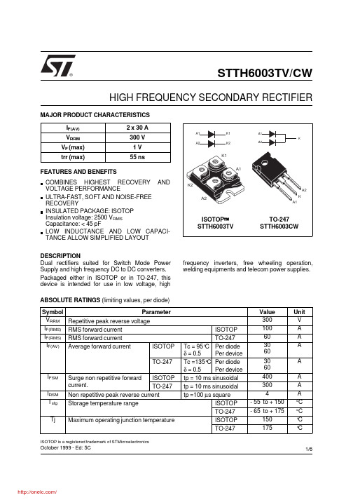
STTH6003TV/CWOctober 1999 - Ed: 5CHIGH FREQUENCY SECONDARY RECTIFIER®Dual rectifiers suited for Switch Mode Power Supply and high frequency DC to DC converters.Packaged either in ISOTOP or in TO-247, this device is intended for use in low voltage, high frequency inverters, free wheeling operation,welding equipments and telecom power supplies.DESCRIPTIONCOMBINES HIGHEST RECOVERY AND VOLTAGE PERFORMANCEULTRA-FAST, SOFT AND NOISE-FREE RECOVERYINSULATED PACKAGE: ISOTOP Insulation voltage: 2500 V RMS Capacitance: < 45 pFLOW INDUCTANCE AND LOW CAPACI-TANCE ALLOW SIMPLIFIED LAYOUT FEATURES AND BENEFITSSymbol ParameterValue Unit V RRM Repetitive peak reverse voltage 300V I F(RMS)RMS forward current ISOTOP 100A I F(RMS)RMS forward current TO-24760A I F(AV)Average forward current ISOTOPTc = 95°C δ = 0.5Per diode Per device 3060A TO-247Tc =135°C δ = 0.5Per diode Per device 3060A I FSM Surge non repetitive forward current.ISOTOP tp = 10 ms sinusoidal 400A TO-247tp = 10 ms sinusoidal 300A I RSMNon repetitive peak reverse current tp =100 µs square4A T stg Storage temperature rangeISOTOP - 55 to + 150°C TO-247- 65 to + 175°C TjMaximum operating junction temperatureISOTOP 150°C TO-247175°CABSOLUTE RATINGS (limiting values, per diode)I F(AV) 2 x 30 A V RRM 300 V V F (max) 1 V trr (max)55 nsMAJOR PRODUCT CHARACTERISTICSA1K1K2A2A1A2K1K2ISOTOP ™STTH6003TV ISOTOP is a registered trademark of STMicroelectronicsA1K A2A1A2KTO-247STTH6003CW1/6Symbol Parameter Tests conditionsMin.Typ.Max.Unit I R *Reverse leakage currentV R = 300 VTj = 25°C 60µATj = 125°C60600V F **Forward voltage dropI F = 30 ATj = 25°C 1.25V Tj = 125°C0.851Pulse test : * tp = 5 ms, δ < 2 % ** tp = 380 µs, δ < 2%To evaluate the maximum conduction losses use the following equation:P = 0.75 x I F(AV) + 0.008 x I F 2(RMS)STATIC ELECTRICAL CHARACTERISTICS (per diode)Symbol ParameterValue Unit R th (j-c)Junction to caseISOTOP Per diodeTotal 1.40.75°C/WTO-247Per diode Total 10.55R th (c)Coupling0.1When the diodes 1 and 2 are used simultaneously:∆Tj (diode 1) = P (diode 1) x R th(j-c) (per diode) + P (diode 2) x R th(C)THERMAL RESISTANCES Symbol Tests conditionsMin.Typ.Max.Unit trrI F = 0.5 A Irr = 0.25 A I R = 1A Tj = 25°C40nsI F= 1 A dI F /dt = - 50 A/µs V R = 30 V 55tfr I F = 30 A dI F /dt = 200 A/µs Tj = 25°C 350ns V FP V FR = 1.1 x V F max.5V S factor Vcc = 200 V I F = 30 A Tj = 125°C0.3-I RMdI F /dt = 200 A/µs11A RECOVERY CHARACTERISTICS STTH6003TV/CW2/65101520253035400510152025303540IF(av) (A)P1(W)Tδ=tp/Ttpδ= 1δ= 0.5δ= 0.2δ= 0.1δ= 0.05Fig. 1: Conduction losses versus average current (per diode).0.20.40.60.81.01.21.41.61.82.02.22.42.6110100VFM(V)IFM(A)Tj=125°C T ypical valuesTj=25°C Maximum valuesTj=125°C Maximum valuesFig. 2: Forward voltage drop versus forward current (maximum values , per diode).05010015020025030035040045050020406080100120140160180trr(ns)VR=200V Tj=125°CIF=2*IF(av)IF=IF(av)IF=0.5*IF(av)dIF/dt(A/µs)Fig. 5: Reverse recovery time versus dI F /dt (90%confidence, per diode).50100150200250300350400450500246810121416182022dIF/dt(A/µs)IRM(A)VR=200V Tj=125°CIF=2*IF(av)IF=IF(av)IF=0.5*IF(av)Fig. 4: Peak reverse recovery current versus dI F /dt (90% confidence, per diode).1E-31E-21E-11E+01E+10.00.20.40.60.81.0tp(s)Zth(j-c)/Rth(j-c)Tδ=tp/TtpSingle pulse δ= 0.5δ= 0.2δ= 0.1Fig. 3a: Relative variation of thermal impedance junction to case versus pulse duration (ISOTOP).1E-41E-31E-21E-11E+00.00.20.40.60.81.0Zth(j-c)/Rth(j-c)Tδ=tp/Ttptp(s)Single pulseδ= 0.5δ= 0.2δ= 0.1Fig. 3b: Relative variation of thermal impedance junction to case versus pulse duration (TO-247).STTH6003TV/CW3/62550751001250.00.20.40.60.81.01.21.41.61.82.02.22.4Tj(°C)IRMS factorFig. 7: Relative variation of dynamic parameters versus junction temperature (reference: Tj = 125°C).50100150200250300350400450500246810VFP(V)IF=IF(av)Tj=125°CdIF/dt(A/µs)Fig. 8: Transient peak forward voltage versus dI F /dt (90% confidence, per diode).050100150200250300350400450500100200300400500tfr(ns)IF=IF(av)VFR=1.1*VFmaxTj=125°CdIF/dt(A/µs)Fig. 9: Forward recovery time versus dI F /dt (90%confidence, per diode).0501001502002503003504004505000.00.10.20.30.40.50.6S factor VR=200V Tj=125°CdIF/dt(A/µs)Fig. 6: Softness factor (tb/ta) versus dI F /dt (typical values, per diode).STTH6003TV/CW4/6PACKAGE MECHANICAL DATA ISOTOPREF.DIMENSIONS Millimeters Inches Min.Max.Min.Max.A11.8012.200.4650.480 A18.909.100.3500.358 B7.88.200.3070.323 C0.750.850.0300.033 C2 1.95 2.050.0770.081 D37.8038.20 1.488 1.504 D131.5031.70 1.240 1.248 E25.1525.500.990 1.004 E123.8524.150.9390.951 E224.80 typ.0.976 typ.G14.9015.100.5870.594 G112.6012.800.4960.504 G2 3.50 4.300.1380.169 F 4.10 4.300.1610.169 F1 4.60 5.000.1810.197 P 4.00 4.300.1570.69P1 4.00 4.400.1570.173 S30.1030.30 1.185 1.193STTH6003TV/CW5/6Information furnished is believed to be accurate and reliable. However, STMicroelectronics assumes no responsibility for the consequences of use of such information nor for any infringement of patents or other rights of third parties which may result from its use. No license is granted by implication or otherwise under any patent or patent rights of STMicroelectronics. Specifications mentioned in this publication are subject to change without notice. This publication supersedes and replaces all information previously supplied.STMicroelectronics products are not authorized for use as critical components in life support devices or systems without express written ap-proval of STMicroelectronics.The ST logo is a registered trademark of STMicroelectronics © 1999 STMicroelectronics - Printed in Italy - All rights reserved.STMicroelectronics GROUP OF COMPANIESAustralia - Brazil - China - Finland - France - Germany - Hong Kong - India - Italy - Japan - MalaysiaMalta - Morocco - Singapore - Spain - Sweden - Switzerland - United Kingdom - U.S.A.PACKAGE MECHANICAL DATA TO-247F2F1V2L4L2L1L3DLL5MEHVVADia.F3F4G = =F(x3)REF.DIMENSIONSMillimeters Inches Min.Typ.Max.Min.Typ.Max.A 4.85 5.150.1910.203D 2.20 2.600.0860.102E 0.400.800.0150.031F 1.00 1.400.0390.055F1 3.000.118F2 2.000.078F3 2.00 2.400.0780.094F4 3.00 3.400.1180.133G 10.900.429H 15.4515.750.6080.620L 19.8520.150.7810.793L1 3.70 4.300.1450.169L218.500.728L314.2014.800.5590.582L434.60 1.362L5 5.500.216M 2.00 3.000.0780.118V 5°5°V260°60°Dia. 3.55 3.650.1390.143Ordering code Marking Package Weight Base qty Delivery modeSTTH6006TV1STTH6006TV ISOTOP 27gwithout screws10with screwsTubeSTTH6006CW STTH6006CW TO-247 4.36g30TubeCooling method: by conduction (C)Recommended torque value (ISOTOP): 1.3 N.m.Recommended torque value (TO-247°: 0.8 N.m.Maximum torque value (ISOTOP): 1.5 N.m.Maximum torque value (TO-247): 1.0 N.m.Epoxy meets UL 94,V0STTH6003TV/CW6/6分销商库存信息: STMSTTH6003CW。
4684;中文规格书,Datasheet资料

Pomona®All dimensions are in inches. Tolerances (except noted): .xx = ±.02” (,51 mm), .xxx = ± .005” (,127 mm).All specifications are to the latest revisions. Specifications are subject to change without notice.Registered trademarks are the property of their respective companies. Made in USA6/9/99Pomona ACCESS 90601 (800) 444-6785 or (425) 446-6010 SY/EH/LS More drawings available at Page 1 of 1 Model 4684 Adapter – BNC Female To Banana Plug With Ground LeadSales: 800-490-2361 Fax: 888-403-3360 Technical Assistance: 800-241-2060 FEATURES:• Permits BNC male to be used with equipment having standard banana jacks.• Allows the ground jack to be located up to 63,5 (2.50) away from the output/input jack.MATERIALS:Upper Conn: BNC FemaleFinish: Body – Tarnish resistant.Center Contact – Gold plated per requirements of MIL-C-39012.Insulation: Polypropylene molded to connector, plug body and wire.Color: Red.Marking: “POMONA 4684.”Ground Lead: In-line Banana Plug. Spring – Beryllium Copper per QQ-C-533, Alloy 172,Cond. H.T.Material: Body – Brass per QQ-B-626, Alloy 360, ½ Hard.Finish: Nickel plated per QQ-N-290, Class 2, 200/300 microinches.Wire: 18 AWG, stranding 65 x 36 t.c., PVC insulated, 3.66 (.144) O.D.Color: BlackBanana Plug Insulation: Polypropylene molded to plug body and wire.Color: Black.Lower Conn: Banana PlugMaterial: Spring – Beryllium Copper per QQ-C-533, Alloy 172, Cond. H.T.Body – Brass per QQ-B-626, Alloy 360, ½ Hard.Finish: Nickel plated per QQ-N-290, Class 2, 200/300 microinches.RATINGS:Operating Temperature: +55º C. (+131º F.) Max.Voltage: Hand-held Testing: 30VAC/60VEDC Max.Hand Free Testing in Controlled Voltage Environments: 500 VRMS Max.ORDERING INFORMATION: Model 4684/分销商库存信息: POMONA4684。
热解碳涂层石墨产品说明书
化学品安全技术说明书物品名称: 热解碳涂层石墨; Pyrolytic Carbon Coated Graphite 修正日期: 2022-07-15 符合GB/T 16483和GB/T 17519标准SDS ID: 0152 (CHINA)版本 3.0物品名称热解碳涂层石墨; Pyrolytic Carbon Coated Graphite供应商的详细情况当地信息 (Local information):艾微美科材国际贸易(上海)有限公司ATMI International Trading Co,LTD上海市科苑路88号德国中心二号楼523-533室Unit 523-533, Tower 2, German Center, No.88 Keyuan Road, Shanghai 201203, China 邮政编码:201203Zip Code: 201203电话:86-21-80236500Telephone: 86-21-80236500应急电话:Emergency Call:86-21-80236500 (上海)1-703-527-3887 (国际)86-532-83889090 (中国,24 小时应急电话)电子邮箱:********************************产品用途半导体和工业应用使用限制不明。
分类标准对其未作要求标签要素象形图分类标准对其未作要求信号词分类标准对其未作要求危险性说明分类标准对其未作要求。
防范说明预防措施分类标准对其未作要求。
事故响应分类标准对其未作要求。
安全储存分类标准对其未作要求。
废弃处置按照地方/区域/国家/国际规章处置内装物/容器。
物理和化学危险无相关数据健康危害无相关数据环境危害无相关数据分类未包括的其它危险性不明。
吸入如果发生不利影响,转移到无污染的地方。
如果没有呼吸给人工呼吸。
立即就医。
接触皮肤用肥皂和水清洗皮肤至少15分钟同时脱去污染了的衣服和鞋子。
DSEI60-06A;中文规格书,Datasheet资料

166 W
0.8...1.2 Nm
6
g
Symbol
IR
VF
VT0 rT RthJC RthCH trr IRM
Conditions
Characteristic Values typ. max.
VR = VRRM VR = 0.8·VRRM VR = 0.8·VRRM
TVJ = 25°C TVJ = 25°C TVJ = 125°C
IXYS reserves the right to change limits, test conditions and dimensions
© 2007 IXYS All rights reserved
/
0549
2-2
Dimensions TO-247 AD
C
D
t = 8.3 ms (60 Hz), sine
TC = 25°C mounting torque typical
Maximum Ratings
100 A 60 A
550 A 600
480 A 520Biblioteka 1510 A2s 1490
1150 A2s 1120
-55...+150 °C 150 °C
-55...+150 °C
Fast Recovery Epitaxial Diode (FRED)
DSEI60-06A DSEI60-06AT
IFAV = 60 A VRRM = 600 V trr = 35 ms
VRSM V
600 600
VRRM V
600 600
Type
DSEI 60-06A DSEI 60-06AT
A
0736440216;中文规格书,Datasheet资料

This document was generated on 08/09/2012PLEASE CHECK FOR LATEST PART INFORMATIONPart Number:73644-0216Status:ActiveOverview:HDM®Description:2.00mm Pitch HDM® Board-to-Board Backplane Header, Vertical, SMC, Press-Fit,Guide Post Location B, Polarizing Key Position N/A, 72 CircuitsDocuments:3D ModelTest Summary TS-73670-990 (PDF)Drawing (PDF)RoHS Certificate of Compliance (PDF)Agency CertificationCSA LR19980ULE29179GeneralProduct Family Backplane Connectors Series73644Application BackplaneCommentsStandard Press-Fit Component Type PCB Header OverviewHDM®Product Name HDM®Style N/AUPC800755022940PhysicalCircuits (Loaded)72Circuits (maximum)72Color - ResinBlack, Natural Durability (mating cycles max)250First Mate / Last Break No Flammability94V-0Guide to Mating Part Yes Keying to Mating Part NoneMaterial - MetalPhosphor Bronze, Stainless Steel Material - Plating MatingGold Material - Plating Termination GoldMaterial - Resin High Temperature Thermoplastic Net Weight5.610/g Number of Columns 12Number of Pairs Open Pin Field Number of Rows 6Orientation Vertical PC Tail Length 3.50mm PCB Locator No PCB RetentionYes PCB Thickness - Recommended 2.50mm Packaging TypeTube Pitch - Mating Interface2.00mm Pitch - Termination Interface 2.00mm Plating min - Mating0.762µm Plating min - Termination 0.051µm Polarized to PCB No StackableNo Surface Mount Compatible (SMC)YesTemperature Range - Operating-55°C to +105°CSeriesimage - Reference onlyEU RoHSChina RoHSELV and RoHS Compliant REACH SVHCContains SVHC: No Low-Halogen Status Not ReviewedNeed more information on product environmental compliance?Email productcompliance@For a multiple part number RoHS Certificate of Compliance, click herePlease visit the Contact Us section for any non-product compliance questions.Search Parts in this Series 73644SeriesMates With73632 HDM PLUS® Board-to-Board Daughtercard Receptacle. 73780 HDM®Board-to-Board Daughtercard Receptacle Application Tooling | FAQTooling specifications and manuals are found by selecting the products below.Crimp Height Specifications are then contained in the Application Tooling Specification document.GlobalDescription Product #Extraction Tool 0621001000Backplane Insertion Signal Contact Tool0621001400Flat Rock Tooling for Pneumatic Press0622013700Termination Interface: Style Through Hole - Compliant PinElectricalCurrent - Maximum per Contact1AData Rate 1.0 GbpsReal Signals (per 25mm)75Shielded NoVoltage - Maximum250V ACMaterial InfoReference - Drawing NumbersSales Drawing SDA-73644-****Test Summary TS-73670-990HDM and High Density Metric are trademarks of Amphenol CorporationThis document was generated on 08/09/2012PLEASE CHECK FOR LATEST PART INFORMATION分销商库存信息: MOLEX 0736440216。
0440670802;中文规格书,Datasheet资料

This document was generated on 08/20/2012PLEASE CHECK FOR LATEST PART INFORMATIONPart Number:44067-0802Status:ActiveOverview:Micro-Fit 3.0™ ConnectorsDescription:3.00mm Pitch Micro-Fit 3.0™ Wire-to-Board Header, Dual Row, Vertical for up to 3.56mm Thick PCB, 8 Circuits, 0.38µm Gold (Au) Selective PlatingDocuments:3D ModelTest Summary TS-43045-002 (PDF)Drawing (PDF)RoHS Certificate of Compliance (PDF)Product Specification PS-43045 (PDF)GeneralProduct Family PCB Headers Series44067Application Power, Wire-to-BoardComments High Temperature, Polarization Key to PCB OverviewMicro-Fit 3.0™ Connectors Product Name Micro-Fit 3.0™UPC800753925571PhysicalBreakawayNo Circuits (Loaded)8Circuits (maximum)8Color - ResinBlack Durability (mating cycles max)30First Mate / Last Break No Glow-Wire Compliant No Guide to Mating Part No Keying to Mating Part None Lock to Mating PartYes Material - Plating MatingGold Material - Plating Termination TinMaterial - Resin High Temperature Thermoplastic Net Weight1.241/g Number of Rows 2Orientation Vertical PC Tail Length 4.01mm PCB Locator Yes PCB RetentionYes PCB Thickness - Recommended 3.60mm Packaging TypeTray Pitch - Mating Interface3.00mm Pitch - Termination Interface 3.00mm Plating min - Mating0.381µm Plating min - Termination 2.540µm Polarized to PCB Yes Shrouded Fully StackableNo Surface Mount Compatible (SMC)YesTemperature Range - Operating -40°C to +105°CTermination Interface: StyleThrough Hole - Kinked Pin ElectricalCurrent - Maximum per Contact 5A Voltage - Maximum250VSeriesimage - Reference onlyEU RoHSChina RoHSELV and RoHS Compliant REACH SVHCContains SVHC: No Low-Halogen Status Low-HalogenNeed more information on product environmental compliance?Email productcompliance@For a multiple part number RoHS Certificate of Compliance, click herePlease visit the Contact Us section for any non-product compliance questions.Search Parts in this Series 44067SeriesMates With43025 Micro-Fit™ HeaderSolder Process DataDuration at Max. Process Temperature (seconds)30Lead-free Process Capability SMC & Wave Capable (TH only)Max. Cycles at Max. Process Temperature3Process Temperature max. C260Material InfoReference - Drawing NumbersProduct Specification PS-43045Sales Drawing SD-44067-001Test Summary TS-43045-002This document was generated on 08/20/2012PLEASE CHECK FOR LATEST PART INFORMATION分销商库存信息: MOLEX 0440670802。
ZXMS6004DGTA;中文规格书,Datasheet资料

60V N-channel self protected enhancement mode Intellifet MOSFETSummaryContinuous drain source voltage60 VOn-state resistance500 mΩNominal load current (V IN = 5V) 1.3 AClamping energy490mJDescriptionThe ZXMS6004DG is a self protected low side MOSFET with logic levelinput. It integrates over-temperature, over-current, over-voltage (activeclamp) and ESD protected logic level functionality. The ZXMS6004DG isideal as a general purpose switch driven from 3.3V or 5Vmicrocontrollers in harsh environments where standard MOSFETs arenot rugged enough.Features•Compact high power dissipation package•Low input current•Logic Level Input (3.3V and 5V)•Short circuit protection with auto restart •Over voltage protection (active clamp)•Thermal shutdown with auto restart •Over-current protection•Input Protection (ESD)•High continuous current rating Ordering informationDevice Part mark Reel size(inches)Tape width(mm)Quantity per reelZXMS66004DGTA ZXMS6004D712 embossed3,000 unitsApplication information•Especially suited for loads with a high in-rush current such as lamps and motors.•All types of resistive, inductive and capacitive loads in switching applications.•μC compatible power switch for 12V and 24V DC applications.•Automotive rated.•Replaces electromechanical relays and discrete circuits.•Linear Mode capability - the current-limiting protection circuitry is designed to de-activate at low V DS to minimise on state power dissipation. The maximum DC operating current is therefore determined by the thermal capability of the package/board combination, rather than by the protection circuitry. This does not compromise the product’s ability to self-protect at low V DS.Absolute maximum ratingsThermal resistanceNOTES(a)For a device surface mounted on a 15mm x 15mm single sided 1oz weight copper on 1.6mm FR4 board, in still air conditions.(b)F or a device surface mounted on 50mm x 50mm single sided 2oz weight copper on 1.6mm FR4 board in still air conditions.(c)Thermal resistance from junction to the mounting surface of the drain pin.ParameterSymbol Limit Unit Continuous Drain-Source voltageV DS 60V Drain-Source voltage for short circuit protection V DS(SC)36V Continuous input voltage V IN -0.5 ... +6V Continuous input current -0.2V ≤V IN ≤6VV IN <-0.2V or V IN >6VI INNo limit │I IN │≤2mAOperating temperature range T j ,-40 to +150°C Storage temperature range T stg -55 to +150°C Power dissipation at T A =25°C (a)Linear derating factorP D 1.310.4W mW/°C Power dissipation at T A =25°C (b) Linear derating factorP D 3.024W mW/°C Pulsed drain current @ V IN =3.3V I DM 2A Pulsed drain current @ V IN =5VI DM 2.5A Continuous source current (Body Diode) (a)I S 1A Pulsed dource current (Body Diode) I SM 5A Unclamped single pulse inductive energy, Tj=25°C, I D =0.5A, V DD =24VE AS 490mJ Electrostatic discharge (Human body model)V ESD 4000V Charged device modelV CDM 1000VParameterSymbo Value Unit Junction to ambient (a)R θJA 96°C/W Junction to ambient (b)R θJA 42°C/W Junction to case (c)R θJC12°C/WRecommended operating conditionsThe ZXMS6004DG is optimised for use with µC operating from 3.3V and 5V supplies.CharacteristicsSymbolDescriptionMinMaxUnitsV IN Input voltage range0 5.5V T A Ambient temperature range-40125°C V IH High level input voltage for MOSFET to be on 3 5.5V V IL Low level input voltage for MOSFET to be off00.7V V PPeripheral supply voltage (voltage to which load is referred)36VElectrical characteristics (at T amb = 25°C unless otherwise stated).Notes:(d)The drain current is restricted only when the device is in saturation (see graph ‘typical output characteristic’). This allows the device to be used in the fully on state without interference from the current limit. The device is fully protected at all drain currents, as the low power dissipation generated outside saturation makes current limit unnecessary.ParameterSymbol Min Typ Max Unit ConditionsStatic Characteristics Drain-Source clamp voltage V DS(AZ)606570V I D =10mA Off-state drain Ccrrent I DSS 500nA V DS =12V, V IN =0V Off-state drain current I DSS 1μA V DS =36V, V IN =0V Input threshold voltage V IN(th)0.71 1.5V V DS =V GS , I D =1mA Input current I IN 60100μA V IN =+3V Input currentI IN120200μA V IN =+5V Input current while over temperature active400μA V IN =+5VStatic Drain-Source on-state resistanceR DS(on)400600m ΩV IN =+3V, I D =0.5A Static Drain-Source on-state resistanceR DS(on)350500m ΩV IN =+5V, I D =0.5A Continuous drain current (a) I D 0.9A V IN =3V; T A =25°C Continuous drain cCurrent(a)I D 1.0A V IN =5V; T A =25°C Continuous drain current (b)I D 1.2A V IN =3V; T A =25°C Continuous drain current (b)I D 1.3AV IN =5V; T A =25°C Current limit I D(LIM)0.7 1.7A V IN =+3V,Current limit (c)I D(LIM)12.2A V IN =+5VDynamic characteristics Turn-on delay time t d(on)5μs V DD =12V, I D =0.5A, V GS =5VRise timet r 10μs Turn-off delay time t d(off)45μs Fall time f f15μsElectrical characteristics - continuedNote:(a)Over-temperature protection is designed to prevent device destruction under fault conditions. Fault conditions are considered as “outside” normal operating range, so this part is not designed to withstand over-temperature for extended periods..ParameterSymbolMinTypMaxUnitConditionsOver-temperature protection Thermal overload trip temperature (a)TJT150175°C Thermal hysteresis (a)10°CTypical characteristicsPackage information - SOT223Note: Controlling dimensions are in millimeters. Approximate dimensions are provided in inchesDim.Millimeters Inches limeters InchesMin.Max.Min.Max.Min.Max.Min.Max.A - 1.8-0.071D 6.30 6.700.2480.264A10.020.10.00080.004e 2.30 BSC 0.0905 BSC A2 1.55 1.650.06100.0649e1 4.60 BSC 0.181 BSC b 0.660.840.0260.033E 6.707.300.2640.287b2 2.90 3.100.1140.122E1 3.30 3.700.1300.146C0.230.330.0090.013L0.90-0.355-Sales officesThe Americas3050 E. Hillcrest Drive Westlake Village,CA 91362-3154Tel: (+1) 805 446 4800 Fax: (+1) 805 446 4850EuropeKustermann-ParkBalanstraße 59,D-81541 MünchenGermanyTel: (+49) 894 549 490Fax: (+49) 894 549 4949Taiwan7F, No. 50,Min Chuan RoadHsin-TienTaipei, TaiwanTel: (+886) 289 146 000Fax: (+886) 289 146 639ShanghaiRm. 606, No.1158Changning RoadShanghai, ChinaTel: (+86) 215 241 4882Fax (+86) 215 241 4891ShenzhenANLIAN Plaza, #4018Jintian RoadFutian CBD,Shenzhen, ChinaTel: (+86) 755 882 849 88Fax: (+86) 755 882 849 99Korea6 Floor, Changhwa B/D,1005-5 Yeongtong-dong,Yeongtong-gu, Suwon-si,Gyeonggi-do, Korea 443-813Tel: (+82) 312 731 884Fax: (+82) 312 731 885DefinitionsProduct changeDiodes Incorporated reserves the right to alter, without notice, specifications, design, price or conditions of supply of any product or service. Customers are solely responsible for obtaining the latest relevant information before placing orders.Applications disclaimerThe circuits in this design/application note are offered as design ideas. It is the responsibility of the user to ensure that the circuit is fit for the user’s application and meets with the user’s requirements. No representation or warranty is given and no liability whatsoever is assumed by Diodes Inc. with respect to the accuracy or use of such information, or infringement of patents or other intellectual property rights arising from such use or otherwise. Diodes Inc. does not assume any legal responsibility or will not be held legally liable (whether in contract, tort (including negligence), breach of statutory duty, restriction or otherwise) for any damages, loss of profit, business, contract, opportunity or consequential loss in the use of these circuit applications, under any circumstances.Life supportDiodes Zetex products are specifically not authorized for use as critical components in life support devices or systems without the express written approval of the Chief Executive Officer of Diodes Incorporated. As used herein:A. Life support devices or systems are devices or systems which:1.are intended to implant into the bodyor2.support or sustain life and whose failure to perform when properly used in accordance with instructions for use provided in thelabeling can be reasonably expected to result in significant injury to the user.B. A critical component is any component in a life support device or system whose failure to perform can be reasonably expected tocause the failure of the life support device or to affect its safety or effectiveness.ReproductionThe product specifications contained in this publication are issued to provide outline information only which (unless agreed by the company in writing) may not be used, applied or reproduced for any purpose or form part of any order or contract or be regarded as a representation relating to the products or services concerned.Terms and ConditionsAll products are sold subjects to Diodes Inc. terms and conditions of sale, and this disclaimer (save in the event of a conflict between the two when the terms of the contract shall prevail) according to region, supplied at the time of order acknowledgement.For the latest information on technology, delivery terms and conditions and prices, please contact your nearest Diodes Zetex sales office.Quality of productDiodes Zetex Semconductors Limited is an ISO 9001 and TS16949 certified semiconductor manufacturer.To ensure quality of service and products we strongly advise the purchase of parts directly from Diodes Inc. or one of our regionally authorized distributors. For a complete listing of authorized distributors please visit: or Diodes Inc. does not warrant or accept any liability whatsoever in respect of any parts purchased through unauthorized sales channels.ESD(Electrostatic discharge)Semiconductor devices are susceptible to damage by ESD. Suitable precautions should be taken when handling and transporting devices. The possible damage to devices depends on the circumstances of the handling and transporting, and the nature of the device. The extent of damage can vary from immediate functional or parametric malfunction to degradation of function or performance in use over time. Devices suspected of being affected should be replaced.Green complianceDiodes Inc. is committed to environmental excellence in all aspects of its operations which includes meeting or exceeding regulatory requirements with respect to the use of hazardous substances. Numerous successful programs have been implemented to reduce the use of hazardous substances and/or emissions.All Diodes Zetex components are compliant with the RoHS directive, and through this it is supporting its customers in their compliance with WEEE and ELV directives.Product status key:“Preview”Future device intended for production at some point. Samples may be available“Active”Product status recommended for new designs“Last time buy (LTB)”Device will be discontinued and last time buy period and delivery is in effect“Not recommended for new designs”Device is still in production to support existing designs and production“Obsolete”Production has been discontinuedDatasheet status key:“Draft version”This term denotes a very early datasheet version and contains highly provisional information, whichmay change in any manner without notice.“Provisional version”This term denotes a pre-release datasheet. It provides a clear indication of anticipated performance.However, changes to the test conditions and specifications may occur, at any time and without notice.“Issue”This term denotes an issued datasheet containing finalized specifications. However, changes tospecifications may occur, at any time and without notice.分销商库存信息: DIODESZXMS6004DGTA。
74435561100;中文规格书,Datasheet资料

74435561100
DATUM / DATE : 2009-11-02 Gurtspezifikation / Tape specification:
G H
SPEICHERDROSSEL WE-HCI POWER-CHOKE WE-HCI
I Rollenspezifikation / tape and reel specification:
74435561100
DATUM / DATE : 2009-11-02
SPEICHERDROSSEL WE-HCI POWER-CHOKE WE-HCI
H Induktivitätskurve / Inductance curve:
Induktivität vs Strom (typ.) Inductance vs Current (typ.)
08-09-29
Geprüft / checked
Kontrolliert / approved
Datum / date
D-74638 Waldenburg · Max-Eyth-Strasse 1 - 3 · Germany · Telefon (+49) (0) 7942 - 945 - 0 · Telefax (+49) (0) 7942 - 945 - 400 http://www.we-online.de
12,00
10,00
8,00
L (µH)
6,00
4,00
2,00
0,00 0 5 10 15 Current (A) 20 25 30 35
Freigabe erteilt / general release:
..................................................................................
- 1、下载文档前请自行甄别文档内容的完整性,平台不提供额外的编辑、内容补充、找答案等附加服务。
- 2、"仅部分预览"的文档,不可在线预览部分如存在完整性等问题,可反馈申请退款(可完整预览的文档不适用该条件!)。
- 3、如文档侵犯您的权益,请联系客服反馈,我们会尽快为您处理(人工客服工作时间:9:00-18:30)。
C
+ 0,1 n1 - 0 (15x)
2,74 `0,1 5,49 `0,1 8,23 `0,1
C
RECOMMENDED PANEL CUT-OUT
i 0,26 A
b
28,8 `0,1
B
B
11,4 `0,1
B
n3,1 `0,05 (2x)
,4 ` R3
10° `1°
i 0,26 B
3 0 ,1
33,32 `0,1
0,4 11,93 + - 0,3 0,4 11,5 + - 0,3
(5:1)
D
D
0,4 8,6 + - 0,3
c
0,17 6,13 + - 0,08 0,25 3,6 + -0
8+ - 0,23
0,02
0,3 47,7 + -0 0,13 33,32 + - 0,12 0 24,79 + - 0,25
APPROVAL # FREIGABE # DEBLOCAGE # AUTORIZACION
APPROVAL # FREIGABE # DEBLOCAGE # AUTORIZACION # APPROVAL
CUSTOMER APPROVAL DATE:
DO NOT ALTER CAD DRAWING BY HAND
CONEC 15-000463
tolerance
dim. in mm
date
drawn appd. norm d-old
scale: material: title:
5:1 see sheet 1
A
APPROVAL # FREIGABE # DEBLOCAGE # AUTORIZACION
A
name
NAME:
TITLE:
09.09.08 15.09.08
THIS DRAWING MAY NOT BE COPIED OR REPRODUCED IN ANY WAY, AND MAY NOT BE PASSED ON TO A THIRD PARTY WITHOUT WRITTEN PERMISSION. OWNERSHIP AND COPYRIGHT OF CONEC GmbH
21.09.09 26.09.08
HS HS
d-old
15K1A268
part no:
A3 sh: 1 (s# FREIGABE # DEBLOCAGE # AUTORIZACION # APPROVAL
rev. description
D
date
name
C
A
THIS DRAWING MAY NOT BE COPIED OR REPRODUCED IN ANY WAY, AND MAY NOT BE PASSED ON TO A THIRD PARTY WITHOUT WRITTEN PERMISSION. OWNERSHIP AND COPYRIGHT OF CONEC GmbH
Schmidt Fischer
D-SUB FEMALE
15pos. SOLDER PIN STRAIGHT with rear spacer clip and hexlocking screw dwg no: Inventor 10 DINR
COMPANY NAME:
5xc 3xb a
Ä3435 Ä 3129 Origin
Schmidt Fischer
P.C.B. HOLE DRILLINGS
PANEL CUT-OUT D-SUB Female 15pos. Solder pin straight dwg no: Inventor 10 DINR
COMPANY NAME:
1xb a
Ä 3129 Origin
26.09.08
F
E
D
C
B
A
b
c
NOTES:
1. FOR WAVESOLDERING (SOLDER BATH TEMPERATURE 265°C FOR 8 SEC. AND SOLDER PREHEAT 150°C FOR 180 SEC.) 2. IP RATING: IP 67 3. SEALED TO WITHSTAND PRESSURE UP TO 1,45 PSI FOR 30 MINUTES AFTER HIGH TEMPERATURE EXPOSURE 4. METALSHELL: ZINC DIE CAST; min. 50µin NICKEL PLATING over COPPER 5. INSULATORS: PBT GF UL 94 V-0, BLACK 6. O-RING: SILICONE PER ASTM D2000 70 SHORE A 7. SEALING COMPOUND: EPOXY RESIN UL 94 V-0; BLACK 8. CONTACTS: COPPER ALLOY PLATING (SEE PART NO): o PLEASE ADD 1 for 30µin HARD GOLD over min. 50µin NICKEL o PLEASE ADD 3 for 8µin HARD GOLD over min. 50µin NICKEL 9. REAR SPACER CLIPS: COPPER ALLOY; min. 200µin TIN over 80µin NICKEL PCB-HOLE: n3,1`0,1; PCB THICKNISS 1,6mm 10. HEXLOCKING SCREWS: STAINLESS STEEL 11. PCB-HOLE DRILLINGS and RECOMMENDED PANEL CUT-OUT ON SHEET 2 12. RECOMMENDED TORQUE FOR MOUNTING SCREW 35Ncm (3.1 in.LB) / max.67Ncm (6 in.LB) 13. CONNECTOR IS PART MARKED: 15-00046o CONEC ABC
tolerance
dim. in mm
date
drawn appd. norm
scale: material: title:
2:1 (5:1)
APPROVAL # FREIGABE # DEBLOCAGE # AUTORIZACION
see notes
A
A
name
NAME:
TITLE:
09.09.08 15.09.08
15-00046 o
/
F
E
B
F
E
D
C
B
A
D
D
P.C.B. HOLE DRILLINGS
0,13 33,32 + - 0,12
9,6 `0,1 6,86 `0,1 4,11 `0,1
1,42 `0,1 2,84 `0,1
n3,1 `0,1 (2x)
1,37 `0,1
1
c
C
C
0,3 21,1 + -0
10°
n0,64 `0,05 (15x)
c
B
O-RING
SEALING COMPOUND
15-00046o CONEC ABC
B
SEE NOTE 13
b
4,6 9,4
4-40 UNC
4-40 UNC
c
SW 4,8
AT ALL TIMES WATER RESISTANT CONNECTORS NOT IN USE SHOULD BE COVERED WITH A CONEC WATER RESISTANT CAP OR WATER TIGHT HOOD.
HS
15K1A268
part no:
A3 sh: 2
A
APPROVAL # FREIGABE # DEBLOCAGE # AUTORIZACION # APPROVAL
rev. description
D
date
name
C
see sheet 1
/
F
E
B
分销商库存信息:
APPROVAL # FREIGABE # DEBLOCAGE # AUTORIZACION
APPROVAL # FREIGABE # DEBLOCAGE # AUTORIZACION # APPROVAL
CUSTOMER APPROVAL DATE:
DO NOT ALTER CAD DRAWING BY HAND