TD82795 datasheet
EG8405datasheet_V1.0
3W防失真、超低EMI立体声D类音频功放版本变更记录3W防失真、超低EMI立体声D类音频功放目录1. 特点 (3)2. 概述 (3)3. 应用领域 (4)4. 引脚 (4)4.1. 引脚定义 (4)4.2. 引脚描述 (4)5. 结构框图 (5)6. 典型应用电路 (6)7. 电气特性 (6)7.1 极限参数 (6)7.2 典型参数 (7)7.3 直流特性 (7)7.4 交流特性 (7)7.5 模拟特性 (8)8. 应用信息 (8)8.1工作模式 (8)8.2防失真功能(NCN) (9)8.3电源退耦 (10)8.4输入电容 (10)8.5模拟基准旁路电容(C BYP) (10)8.6电源开启/关闭时噼噗噪声 (11)8.7欠压锁定(UVLO) (11)8.8短路电流保护(SCP) (11)8.9过温保护(OTP) (11)8.10电磁辐射(EMI) (11)9. 封装尺寸 (12)3W防失真、超低EMI立体声D类音频功放EG8405芯片数据手册V1.01. 特点⏹防失真功能⏹宽的工作电源2.5V-5.5V⏹超优异的全带宽EMI抑制性能⏹免LC滤波器数字调制,直接驱动扬声器⏹高输出功率:3.0W@PVDD=VDD=5.0V,R L=4Ω,THD+N=10%⏹高效率:88%@PVDD=VDD=5.0V, R L=4Ω,P O=1W⏹低THD+N:0.1%@PVDD=VDD=5.0V, R L=4Ω,P O=1W⏹通道隔离度:80dB@f IN=1KHz,A V=18dB⏹高信噪比SNR: 90dB@ PVDD=VDD=5.0V, A V=18dB⏹优异的“噼噗-咔嗒”(Pop-Click)噪声抑制性能⏹关断功能⏹过流保护功能⏹过热保护功能⏹欠压保护功能⏹无铅SOP16封装2. 概述EG8405是一款带防失真功能且具有超低EMI的立体声免输出滤波器D类音频功率放大器。
在电源电压5V、THD+N=10%、4Ω负载的条件下,输出高达3W的功率,在性能与AB类放大器相媲美的同时,效率高达88%。
LM7905_DataSheet
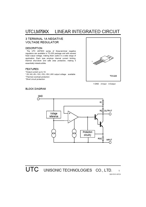
UTC LM79XXLINEAR INTEGRATED CIRCUITUTC UNISONIC TECHNOLOGIES CO., LTD.1QW-R101-007,B3 TERMINAL 1A NEGATIVE VOLTAGE REGULATORDESCRIPTIONThe UTC LM79XX series of three-terminal negativeregulators are available in TO-220 package and with several fixed output voltage, making them useful in a wide range of application. Each type employs internal current limiting, thermal shut-down and safe area protection, making it essentially indestructible.FEATURES*Output current up to 1A*-5V;-6V;-8V;-12V;-15V;-18V;-24V output voltage available *Thermal overload protection *Short circuit protection1:GND 2:Input 3:OutputBLOCK DIAGRAMUTC LM79XXLINEAR INTEGRATED CIRCUITUTC UNISONIC TECHNOLOGIES CO., LTD.2QW-R101-007,BABSOLUTE MAXIMUM RATINGS (Ta=25°C) PARAMETER SYMBOLVALUE UNITInput voltageVi -35 V Thermal resistance junction-airR θ JA 65 °C /W Thermal resistance junction-casesR θ JC 5 °C /W Operating Temperature Topr 0 ~ +125 °C Storage TemperatureTstg-65 ~ +150°CUTC7905 ELECTRICAL CHARACTERISTICS(Refer to test circuits, 0<Tj<125°C ,Io=500mA,Vi=-10V,Ci=33uF,Co=1uF, unless otherwise specified)PARAMETER SYMBOL TEST CONDITIONS MIN TYP MAX UNITTj=25°C-4.80-5.0 -5.20 V Output voltageVo 5.0mA<Io<1.0A,Po<15W Vi=-7V to -20V -4.75 -5.25VLine regulation ∆Vo Tj =25°C,Vi=-7V to -25V 10 100 mV Tj=25°C,Vi=-8V to -12VmV Load regulation ∆Vo Tj =25°C,Io=5.0mA to 1.5A10 100 mV Tj=25°C,Io=250mA to 750mA 3 50 mV Quiescent current I Q Tj=25°C3 6 mA Quiescent current change ∆I QIo=5mA to 1.0A 0.05 0.5 mA Vi=-7V to -25V 0.1 1.3 mA Output voltage drift ∆Vo/∆T Io =5mA -0.4 mV/°C Output noise voltage V N f=10hz to 100kHz,Ta=25°C 100 µV Ripple rejection RR f=120Hz, Vi=-8V to -18V 54 60 dB Dropout voltage Vo Io=1.0A,Tj=25°C 2 V Short circuit current Isc Vi=-35V,Ta=25°C 300 mA peak current Ipk Tj=25°C2.2 AUTC7906 ELECTRICAL CHARACTERISTICS(Refer to test circuits, 0<Tj<125°C ,Io=500mA,Vi=-11V,Ci=2.2uF,Co=1uF,unless otherwise specified)PARAMETER SYMBOL TEST CONDITIONS MIN TYP MAX UNITTj=25°C-5.76-6.00 -6.24 V Output voltageVo5.0mA<Io<1.0A,Po<15W Vi=-8V to -21V -5.70 -6.30 VLine regulation ∆Vo Tj =25°C,Vi=-8V to -25V10 120 mVTj=25°C,Vi=-9V to -13V5 60 mV Load regulation ∆Vo Tj =25°C,Io=5.0mA to 1.5A10 120 mVTj=25°C,Io=250mA to 750mA 3 60 mV Quiescent currentI Q Tj=25°C3 6 mA Quiescent current change ∆I QIo=5mA to 1.0A 0.5 mAVi=-8V to -25V 1.3 mAOutput voltage drift ∆Vo/∆T Io =5mA -0.5 mV/°COutput noise voltage V N f=10hz to 100kHz,Ta=25°C 130 µV Ripple rejection RR f=120Hz, Vi=-9V to -19V 54 60 dB Dropout voltage Vo Io=1.0A,Tj=25°C 2 V Short circuit current Isc Vi=-35V,Ta=25°C 300 mA peak currentIpk Tj=25°C2.2 AUTC LM79XX LINEAR INTEGRATED CIRCUITUTC UNISONIC TECHNOLOGIES CO., LTD.3QW-R101-007,BUTC7908 ELECTRICAL CHARACTERISTICS(Refer to test circuits, 0<Tj<125°C ,Io=500mA,Vi=-14V,Ci=2.2uF,Co=1uF,unless otherwise specified)PARAMETER SYMBOL TEST CONDITIONS MIN TYP MAX UNITTj=25°C-7.68-8.0 -8.32 V Output voltageVo5.0mA<Io<1.0A,Po<15W Vi=-10.5V to -23V -7.60 -8.40 VLine regulation ∆Vo Tj =25°C,Vi=-10.5V to -25V 10 100 mV Tj=25°C,Vi=-11.5V to -17V5 80 mV Load regulation ∆Vo Tj =25°C,Io=5.0mA to 1.5A12 160 mV Tj=25°C,Io=250mA to 750mA4 80 mV Quiescent current I Q Tj=25°C3 6 mA Quiescent current change ∆I QIo=5mA to 1.0A 0.05 0.5 mA Vi=-11.5V to -25V 0.1 1.0 mA Output voltage drift ∆Vo/∆T Io =5mA -0.6 mV/°C Output noise voltage V N f=10hz to 100kHz,Ta=25°C 175 µV Ripple rejection RR f=120Hz, Vi=-11.5V to -21.5V 54 60 dB Dropout voltage Vo Io=1.0A,Tj=25°C 2 V Short citcuit current Isc Vi=-35V,Ta=25°C 300 mA peak current Ipk Tj=25°C2.2 AUTC7912 ELECTRICAL CHARACTERISTICS(Refer to test circuits, 0<Tj<125°C ,Io=500mA,Vi=-18V,Ci=2.2uF,Co=1uF,unless otherwise specified)PARAMETER SYMBOL TEST CONDITIONS MIN TYP MAX UNITTj=25°C-11.52-12.0 -12.48 V Output voltageVo5.0mA<Io<1.0A,Po<15W Vi=-14.5V to -27V -11.40 -12.60 V Line regulation ∆Vo Tj =25°C,Vi=-14.5V to -30V12 240 mVTj=25°C,Vi=-16V to -22V6 120 mV Load regulation ∆Vo Tj =25°C,Io=5.0mA to 1.5A12 240 mVTj=25°C,Io=250mA to 750mA 4 120 mV Quiescent currentI Q Tj=25°C3 6 mA Quiescent current change ∆I QIo=5mA to 1.0A 0.05 0.5 mAVi=-14.5V to -30V 0.1 1.0 mAOutput voltage drift ∆Vo/∆T Io =5mA -0.8 mV/°COutput noise voltage V N f=10hz to 100kHz,Ta=25°C 200 µV Ripple rejection RR f=120Hz, Vi=-15V to -25V 54 60 dB Dropout voltage Vo Io=1.0A,Tj=25°C 2 V Short circuit current Isc Vi=-35V,Ta=25°C 300 mA peak currentIpk Tj=25°C2.2 AUTC LM79XX LINEAR INTEGRATED CIRCUITUTC UNISONIC TECHNOLOGIES CO., LTD.4QW-R101-007,BUTC7915 ELECTRICAL CHARACTERISTICS(Refer to test circuits, 0<Tj<125°C , Io=500mA,Vi=-23V,Ci=2.2uF,Co=1uF,unless otherwise specified)PARAMETER SYMBOL TEST CONDITIONS MIN TYP MAX UNITTj=25°C-14.40-15.0 -15.60 V Output voltageVo5.0mA<Io<1.0A,Po<15W Vi=-17.5V to -30V -14.25 -15.75 VLine regulation ∆Vo Tj =25°C,Vi=-17.5V to -30V 12 300 mV Tj=25°C,Vi=-20V to -26V6 150 mV Load regulation ∆Vo Tj =25°C,Io=5.0mA to 1.5A 12 300 mV Tj=25°C,Io=250mA to 750mA 4 150 mV Quiescent current I Q Tj=25°C3 6 mA Quiescent current change ∆I QIo=5mA to 1.0A 0.05 0.5 mA Vi=-17.5V to -30.5V 0.1 1.0 mA Output voltage drift ∆Vo/∆T Io =5mA -0.9 mV/°C Output noise voltage V N f=10hz to 100kHz,Ta=25°C 250 µV Ripple rejection RR f=120Hz, Vi=-18.5V to -28.5V 54 60 dB Dropout voltage Vo Io=1.0A,Tj=25°C 2 V Short circuit current Isc Vi=-35V,Ta=25°C 300 mA peak current Ipk Tj=25°C2.2 AUTC7918 ELECTRICAL CHARACTERISTICS(Refer to test circuits, 0<Tj<125°C ,Io=500mA,Vi=-27V,Ci=2.2uF,Co=1uF,unless otherwise specified)PARAMETER SYMBOL TEST CONDITIONS MIN TYP MAX UNITTj=25°C-17.28-18.0 -18.72 V Output voltageVo5.0mA<Io<1.0A,Po<15W Vi=-21V to -33V -17.10 -18.90 V Line regulation ∆Vo Tj =25°C,Vi=-21V to -33V15 360 mVTj=25°C,Vi=-24V to -30V8 180 mV Load regulation ∆Vo Tj =25°C,Io=5.0mA to 1.5A15 360 mVTj=25°C,Io=250mA to 750mA 5.0 180 mV Quiescent currentI Q Tj=25°C3 6 mA Quiescent current change ∆I QIo=5mA to 1.0A 0.5 mAVi=-21V to -32V 1.0 mAOutput voltage drift ∆Vo/∆T Io =5mA -1 mV/°COutput noise voltage V N f=10hz to 100kHz,Ta=25°C 300 µV Ripple rejection RR f=120Hz, Vi=-22V to -32V 54 60 dB Dropout voltage Vo Io=1.0A,Tj=25°C 2 V Short circuit current Isc Vi=-35V,Ta=25°C 300 mA peak currentIpk Tj=25°C2.2 AUTC LM79XX LINEAR INTEGRATED CIRCUITUTC UNISONIC TECHNOLOGIES CO., LTD.5QW-R101-007,BUTC7924 ELECTRICAL CHARACTERISTICS(Refer to test circuits, 0<Tj<125°C ,Io=500mA,Vi=-33V,Ci=2.2uF,Co=1uF,unless otherwise specified)PARAMETER SYMBOL TEST CONDITIONS MIN TYP MAX UNITTj=25°C-23.04-24 -24.96 V Output voltageVo5.0mA<Io<1.0A,Po<15W Vi=-27V to -38V -22.80 -25.20 VLine regulation ∆Vo Tj 25°C,Vi=-27V to -38V15 480mVTj=25°C,Vi=-30V to -36V8 240 mV Load regulation ∆Vo Tj 25°C,Io=5.0mA to 1.5A15 480 mVTj=25°C,Io=250mA to 750mA 5.0 240 mV Quiescent currentI Q Tj=25°C3 6 mA Quiescent current change ∆I QIo=5mA to 1.0A 0.5 mAVi=-27V to -38V 1.0 mAOutput voltage drift ∆Vo/∆T Io =5mA -1 mV/°COutput noise voltage V N f=10hz to 100kHz,Ta=25°C 400 µV Ripple rejection RR f=120Hz, Vi=-28V to -38V 54 60 dB Dropout voltage Vo Io=1.0A,Tj=25°C 2 V Short circuit current Isc Vi=-35V,Ta=25°C 300 mA peak currentIpk Tj=25°C2.2 AAPPLICATION CIRCUITSFig.1 Fixed output regulatorFig.2 Split power supply(+-15V,1A)UTC LM79XX LINEAR INTEGRATED CIRCUITFig.3 Circuit for increasing output voltageUTC UNISONIC TECHNOLOGIES CO., LTD. 6QW-R101-007,B。
ADS7825P;ADS7825U;ADS7825UB;ADS7825U1K;ADS7825U1KE4;中文规格书,Datasheet资料

DESCRIPTION
The ADS7825 can acquire and convert 16 bits to within ±2.0 LSB in 25µs max while consuming only 50mW max. Laser-trimmed scaling resistors provide the standard industrial ±10V input range and channelto-channel matching of ±0.1%. The ADS7825 is a low-power 16-bit sampling A/D with a four channel input multiplexer, S/H, clock, reference, and a parallel/serial microprocessor interface. It can be configured in a continuous conversion mode to sequentially digitize all four channels. The 28-pin ADS7825 is available in a plastic 0.3" DIP and in a SOIC, both fully specified for operation over the industrial –40°C to +85°C range.
®
ADS7825
/
2
SPECIFICATIONS (CONT)
ELECTRICAL
At TA = –40°C to +85°C, fS = 40kHz, VS1 = VS2 = V S = +5V ±5%, using external reference, CONTC = 0V, unless otherwise specified. ADS7825P, U PARAMETER DIGITAL TIMING Bus Access Time Bus Relinquish Time Data Clock Internal Clock (Output only when transmitting data) External Clock POWER SUPPLIES VS1 = VS2 = VS Power Dissipation TEMPERATURE RANGE Specified Performance Storage Thermal Resistance (θJA) Plastic DIP SOIC CONDITIONS PAR/SER = +5V PAR/SER = +5V PAR/SER = 0V EXT/INT LOW EXT/INT HIGH MIN TYP MAX 83 83 0.5 0.1 +4.75 fS = 40kHz PWRD HIGH –40 –65 75 75 +5 50 +85 +150 T T T T 1.5 10 +5.25 50 T T T T T T T MIN ADS7825PB, UB TYP MAX T T T T T T UNITS ns ns MHz MHz V mW µW °C °C °C/W °C/W
7905资料

©2011 Fairchild Semiconductor CorporationRev. 1.0.1Features•No External Components Required •Output Current in Excess of 0.5A •Internal Thermal Overload•Internal Short Circuit Current Limiting •Output Transistor Safe Area Compensation•Output V oltages of -5V ,-6V ,-8V , -12V ,-15V ,-18V ,-24VDescriptionThe KA79MXX series of 3-Terminal medium currentnegative voltage regulators are monolithic integrated circuits designed as fixed voltage regulators. These regulators employ internal current limiting, thermal shutdown and safe area compensation making them essentially indestructible.TO-220D-PAK1. GND2. Input3. Output11Schematic DiagramQ1Q2Q3Q4Q5Q6Q7Q8Q9Q10Q11Q12Q13Q14Q15Q16Q17Q18Q19Q20Q21Q22Q23Q24Q25Q26Q27R1R2R3R4R5R6R7R8R9R10R11R12R13R15R14R16R17R18R19R20R21R22R23R24R25D1D2D3D4D5C1C2GNDOUTINKA79MXX3-Terminal 0.5A Negative Voltage RegulatorKA79MXX2Absolute Maximum RatingsElectrical Characteristics (KA79M05/KA79M05R)(Refer to test circuit, 0°C ≤T J ≤ +125°C, l O =350mA, V I =-10V,unless otherwise specified, C I =0.33μF,C O =0.1μF)Note:1. Load and line regulation are specified at constant junction temperature. Change in V O due to heating effects must be takeninto account separately. Pulse testing with low duty is used.ParameterSymbol Value Unit Input Voltage(for V O = -5V to -18V)(for V O = -24V)V I V I -35-40V V Thermal Resistance Junction-Cases R θJC 5°C/W Thermal Resistance Junction-Air R θJA 65°C/W Operating Temperature Range T OPR 0 ~ +125°C Storage Temperature RangeT STG-65 ~ +150°CParameter Symbol ConditionsMin.Typ.Max.UnitOutput VoltageV OT J = +25°C -4.8-5-5.2V I O = 5mA to 350mA V I = -V7 to -25V -4.75-5-5.25Line Regulation (Note1)ΔV O T J =+25°CV I = -7V to -25V -7.050mV V I = -8V to -25V- 2.030Load Regulation (Note1)ΔV O I O = 5mA to 500mA T J = +25°C -30100mV Quiescent Current I Q T J = +25°C - 3.0 6.0mAQuiescent Current Change ΔI Q I O = 5mA to 350mA --0.4mA I O = 200mA V I = -8V to -25V --0.4Output Voltage Drift ΔVo/ΔT I O = 5mA--0.2-mV/°C Output Noise Voltage V N f = 10Hz to 100kHz, T A = +25°C -40-μV Ripple Rejection RR f = 120HzV J = -8Vto -18V 5460-dB Dropout Voltage V D T J =+25°C, I O = 500mA - 1.1-V Short Circuit Current I SC T J = +25°C, V I = -35V -140-mA Peak CurrentI PKT J = +25°C-650-mAKA79MXX3Electrical Characteristics (KA79M06) (Continued)(Refer to test circuit, 0°C ≤T J ≤ +125°C, l O =350mA, V I = -11V,unless otherwise specified)Note:1. Load and line regulation are specified at constant junction temperature. Change in V O due to heating effects must be takeninto account separately. Pulse testing with low duty is used.Parameter SymbolConditionsMin.Typ.Max.UnitOutput VoltageV OT J = +25°C-5.75-6.0-6.25V I O = 5mA to 350mA V I = -8.0V to -25V -5.7-6.0-6.3Line Regulation (Note1)ΔV O T J =+25°C V I = -8Vto -25V -7.060mV V I = -9V to -19V - 2.040Load Regulation (Note1)ΔV O T J = +25°C I O = 5.0mA to 500mA -30120mV Quiescent Current I Q T J = +25°C-36mAQuiescent Current Change ΔI Q I O = 5mA to 350mA --0.4mA V I = -8V to -25V --0.4Output Voltage Drift ΔV O /ΔT I O = 5mA-0.4-mV/°C Output Noise Voltage V N f = 10Hz to 100kHz, T A = +25°C -50-μV Ripple Rejection RR f = 120Hz,V I = -9V to -19V 5460-dB Dropout Voltage V D I O = 500mA, T J = +25°C - 1.1-V Short Circuit Current I SC V I = -35V, T J = +25°C -140-mA Peak CurrentI PKT J = +25°C-650-mAKA79MXX4Electrical Characteristics (KA79M08/KA79M08R) (Continued)(Refer to test circuit, 0°C ≤ T J ≤ +125°C, l O =350mA, V I = -14V,unless otherwise specified)Note:1. Load and line regulation are specified at constant junction temperature. Change in V O due to heating effects must be takeninto account separately. Pulse testing with low duty is used.Parameter SymbolConditionsMin.Typ.Max.UnitOutput VoltageV OT J = +25°C-7.7-8.0-8.3V I O = 5mA to 350mA V I = -10.5V to -25V -7.6-8.0-8.4Line Regulation (Note1)ΔV O T J = +25°C V I = -10.5V to -25V -7.080mV V I = -11V to -21V - 2.050Load Regulation (Note1)ΔV O T J = +25°C I O = 5.0mA to 500mA -30160mV Quiescent Current I Q T J = +25°C -36mAQuiescent Current Change ΔI Q I O = 5mA to 350mA --0.4mA V I = -8V to -25V --0.4Output Voltage Drift ΔV O /ΔT I O = 5mA--0.6-mV/°C Output Noise Voltage V N f = 10Hz to 100kHz, T A = +25°C -60-μV Ripple Rejection RR f = 120Hz,V I = -9V to -19V 5459-dB Dropout Voltage V D I O = 500mA, T J = +25°C - 1.1-V Short Circuit Current I SC V I = -35V, T J = +25°C -140-mA Peak CurrentI PKT J = +25°C-650-mAKA79MXX5Electrical Characteristics (KA79M12) (Continued)(Refer to test circuit, 0°C ≤ T J ≤ +125°C, l O =350mA, V I = -19V,unless otherwise specified)Note:1. Load and line regulation are specified at constant junction temperature. Change in V O due to heating effects must be takeninto account separately. Pulse testing with low duty is used.Parameter SymbolConditionsMin.Typ.Max.UnitOutput VoltageV OT J = +25°C-11.5-12-12.5V I O = 5mA to 350mA V I = -14.5V to -30V -11.4-12-12.6Line Regulation (Note1)ΔV O T J =+25°C V I = -14.5V to -30V -8.080mV V I = -15V to -25V - 3.050Load Regulation (Note1)ΔV O T J = +25°C I O = 5.0mA to 500mA -30240mV Quiescent Current I Q T J = +25°C -36mAQuiescent Current Change ΔI Q I O = 5mA to 350mA --0.4mA V I = -14.5V to -30V --0.4Output Voltage Drift ΔV O /ΔT I O = 5mA--0.8-mV/°C Output Noise Voltage V N f = 10Hz to 100kHz, T A = +25°C -75-μV Ripple Rejection RR f = 120Hz,V I = -15V to -25V 5460-dB Dropout Voltage V D I O = 500mA, T J = +25°C - 1.1-V Short Circuit Current I SC V I = -35V, T J = +25°C -140-mA Peak CurrentI PKT J = +25°C-650-mAKA79MXX6Electrical Characteristics (KA79M15) (Continued)(Refer to test circuit, 0°C ≤ T J ≤ +125°C, l O =350mA, V I = -23V,unless otherwise specified)Note:1. Load and line regulation are specified at constant junction temperature. Change in V O due to heating effects must be takeninto account separately. Pulse testing with low duty is used.Parameter SymbolConditionsMin.Typ.Max.UnitOutput VoltageV OT J = +25°C-14.4-15-15.6V I O = 5mA to 350mA V I = -17.5V to -30V -14.25-15-15.75Line Regulation (Note1)ΔV O T J =+25°C V I = -17.5Vto -30V -9.080mV V I = -18V to -28V - 5.050Load Regulation (Note1)ΔV O T J = +25°C I O = 5.0mA to 500mA -30240mV Quiescent Current I Q T J = +25°C -36mAQuiescent Current Change ΔI Q I O = 5mA to 350mA --0.4mA V I = -17.5V to -28V --0.4Output Voltage Drift ΔV O /ΔT I O = 5mA--1.0-mV/°C Output Noise Voltage V N f = 10Hz to 100kHz, T A = +25°C -90-μV Ripple Rejection RR f = 120Hz,V I = -18.5V to -28.5V 5459-dB Dropout Voltage V D I O = 500mA, T J = +25°C - 1.1-V Short Circuit Current I SC V I = -35V, T J = +25°C -140-mA Peak CurrentI PKT J = +25°C-650-mAKA79MXX7Electrical Characteristics (KA79M18) (Continued)(Refer to test circuit, 0°C ≤ T J ≤ +125°C, l O =350mA, V I = -27V,unless otherwise specified)Note:1. Load and line regulation are specified at constant junction temperature. Change in V O due to heating effects must be takeninto account separately. Pulse testing with low duty is used.Parameter SymbolConditionsMin.Typ.Max.UnitOutput VoltageV OT J = +25°C-17.3-18-18.7V I O = 5mA to 350mA V I = -21V to -33V -17.1-18-18.9Line Regulation (Note1)ΔV O T J =+25°C V I = -21V to -33V -9.080mV V I = -24V to -30V - 5.080Load Regulation (Note1)ΔV O T J = +25°C I O = 5.0mA to 500mA -30360mV Quiescent Current I Q T J = +25°C -36mAQuiescent Current Change ΔI Q I O = 5mA to 350mA --0.4mA V I = -21V to -33V --0.4Output Voltage Drift ΔV O /ΔT I O = 5mA--1.0-mV/°C Output Noise Voltage V N f = 10Hz to 100kHz, T A = +25°C -110-μV Ripple Rejection RR f = 120Hz,V I = -22V to -32V 5459-dB Dropout Voltage V D I O = 500mA, T J = +25°C - 1.1-V Short Circuit Current I SC V I = -35V, T J = +25°C -140-mA Peak CurrentI PKT J = +25°C-650-mAKA79MXX8Electrical Characteristics (KA79M24) (Continued)(Refer to test circuit, 0°C ≤ T J ≤ +125°C, l O =350mA, V I = -33V,unless otherwise specified)Note:1. Load and line regulation are specified at constant junction temperature. Change in V O due to heating effects must be takeninto account separately. Pulse testing with low duty is used.Parameter SymbolConditionsMin.Typ.Max.UnitOutput VoltageV OT J = +25°C-23-24-25V I O = 5mA to 350mA V I = -27V to -38V -22.8-24-25.2Line Regulation (Note1)ΔV O T J =+25°C V I = -27V to -38V -9.080mV V I = -30V to -36V - 5.070Load Regulation (Note1)ΔV O T J = +25°C I O = 5.0mA to 500mA -30300mV Quiescent Current I Q T J = +25°C -36mAQuiescent Current Change ΔI Q I O = 5mA to 350mA --0.4mA V I = -27V to -38V --0.4Output Voltage Drift ΔV O /ΔT I O = 5mA--1.0-mV/°C Output Noise Voltage V N f = 10Hz to 100kHz, T A = +25°C -180-μV Ripple Rejection RR f = 120Hz,V I = -28V to -38V 5458-dB Dropout Voltage V D I O = 500mA, T J = +25°C - 1.1-V Short Circuit Current I SC V I = -35V, T J = +25°C -140-mA Peak CurrentI PKT J = +25°C-650-mAKA79MXX9Typical ApplicationsFigure 1.Fixed Output RegulatorFigure 2.Variable OutputNote:1. Required for stability. For value given, capacitor must be solid tantalum. 25μF aluminum electrolytic may be substituted.2. C 2 improves transient response and ripple rejection. Do not increase beyond 50μF.KA79MXX1.0uF2.0uF312V IV OKA79MXXV OV IR 2R 1C 3SOLIDTANTALUM1uF_+C 12.2uF SOLID TANTALUM_+C 225uF_+KA79MXXMechanical DimensionsPackageDimensions in millimetersTO-22010KA79MXX Mechanical Dimensions (Continued)PackageDimensions in millimetersD-PAK11KA79MXX1/24/11 0.0m 001Stock#DS400023© 2011 Fairchild Semiconductor CorporationLIFE SUPPORT POLICYFAIRCHILD’S PRODUCTS ARE NOT AUTHORIZED FOR USE AS CRITICAL COMPONENTS IN LIFE SUPPORT DEVICES OR SYSTEMS WITHOUT THE EXPRESS WRITTEN APPROVAL OF THE PRESIDENT OF FAIRCHILD SEMICONDUCTOR CORPORATION. As used herein:1.Life support devices or systems are devices or systemswhich, (a) are intended for surgical implant into the body, or (b) support or sustain life, and (c) whose failure to perform when properly used in accordance with instructions for use provided in the labeling, can bereasonably expected to result in a significant injury of the user.2. A critical component in any component of a life supportdevice or system whose failure to perform can bereasonably expected to cause the failure of the life support device or system, or to affect its safety or effectiveness.DISCLAIMERFAIRCHILD SEMICONDUCTOR RESERVES THE RIGHT TO MAKE CHANGES WITHOUT FURTHER NOTICE TO ANY PRODUCTS HEREIN TO IMPROVE RELIABILITY, FUNCTION OR DESIGN. FAIRCHILD DOES NOT ASSUME ANYLIABILITY ARISING OUT OF THE APPLICATION OR USE OF ANY PRODUCT OR CIRCUIT DESCRIBED HEREIN; NEITHER DOES IT CONVEY ANY LICENSE UNDER ITS PATENT RIGHTS, NOR THE RIGHTS OF OTHERS.Ordering InformationProduct NumberPackageOperating TemperatureKA79M05TO-2200 ~ +125°CKA79M06KA79M08KA79M12KA79M15KA79M18KA79M24KA79M05R D-PAK KA79M08R KA79M12R。
BL8052 datasheet v1.0

Symbol Vcc
Vout Icc fOSC RSW VIH VIL
Parameter Breakdown Supply Voltage
Output Voltage Supply Current Shutdown Current Oscillator Frequency Power Efficiency Vcc to Vout Switch Impedance Shutdown Input Threshold SHDN Pin Current
60 50 40 30 20 10 0 0 10 20 30 40 50 60 Vcc=5.5V Vcc=5V Vcc=4.75V Vcc=4.5V Vcc=3.2V
Iout(mA)
OUTPUT VOLTAGE vs. OUTPUT CURRENT
14 12 10
Vout(V)
8 6 4 2 0 0 10 20 30
RECOMMENDED WORK CONDITIONS
Parameter
Input Voltage Range Operating Junction Temperature(TJ)
Value
Max. 6V -20C –125C
ELECTRICAL CHARACTERISTICS For Each Channel
DESCRIPTION
Negative terminal for the first chargepump capacitor Positive terminal for the first chargepump capacitor Negative terminal for the second charge-pump capacitor Positive terminal for the second charge-pump capacitor Supply Voltage +12V Output Voltage. VOUT = VCC when in shutdown mode. Ground Active-high CMOS-logic level Shutdown Input. SHDN is internally pulled up to VCC. Connect to GND for normal peration. In shutdown mode, the charge pumps are turned off and VOUT = VCC.
2SD882;中文规格书,Datasheet资料

October 2007Rev 31/82SD882NPN medium power transistorFeatures■High current■Low saturation voltage ■Complement to 2SB772Applications■Voltage regulation ■Relay driver ■Generic switch ■Audio power amplifier ■DC-DC converterDescriptionThe device is a NPN transistor manufactured by using planar technology resulting in rugged high performance devices. The complementary PNP type is 2SB772.Table 1.Device summaryOrder code Marking Package Packing 2SD882D882SOT -32T ubeAbsolute maximum ratings2SD882 1 Absolute maximum ratingsTable 2.Absolute maximum ratingSymbol Parameter Value UnitV CBO Collector-base voltage (I E = 0) 60VV CEO Collector-emitter voltage (I B = 0) 30VV EBO Collector-base voltage (I C = 0) 5VI C Collector current3AI CM Collector peak current (t P < 5ms)6AI B Base current1AI BM Base peak current (t P < 5ms)2AP TOT T otal dissipation at T c = 25°C12.5WT STG Storage temperature-65 to 150°CT J Max. operating junction temperature150°CTable 3.Thermal dataSymbol Parameter Value UnitR thJ-case Thermal resistance junction-case max10°C/W 2/83/82 Electrical characteristics(T CASE = 25°C; unless otherwise specified)Table 4.Electrical characteristicsSymbol ParameterTest conditions Min.Typ.Max.Unit I CES Collector cut-off current(V BE = 0)V CE = 60 V 10µA I CEO Collector cut-off current (I B = 0)V CE = 30 V 100µA I EBOEmitter cut-off current (I C = 0)V EB = 5 V10µAV (BR)CEO(1)Collector-emitter breakdownvoltage (I B = 0 )I C = 10 mA 30VV (BR)CBO Collector-base breakdownvoltage(I E = 0 )I C = 100 µA60VV (BR)EBO Emitter-base breakdownvoltage(I C = 0 )I E = 100 µA5V V CE(sat)(1)Collector-emitter saturationvoltageI C = 1 A I B = 50 mAI C = 2 A I B = 100 mAI C = 3 A I B = 150 mA 0.40.71.1V V V V BE(sat)(1)1.Pulsed duration = 300 ms, duty cycle ≤1.5%.Base-emitter saturation voltage I C = 2 A I B = 100 mA 1.2Vh FE DC current gain I C = 100 mA V CE = 2 V I C = 1 A V CE = 2 V I C = 3 A V CE = 2 V 1008030300f TTransition frequencyI C = 0.1 A V CE = 10 V100MHzcharacteristics (curves) 2.1 Typical4/82SD882Package mechanical data 3 Package mechanical dataIn order to meet environmental requirements, ST offers these devices in ECOPACK®packages. These packages have a Lead-free second level interconnect . The category ofsecond level interconnect is marked on the package and on the inner box label, incompliance with JEDEC Standard JESD97. The maximum ratings related to solderingconditions are also marked on the inner box label. ECOPACK is an ST trademark.ECOPACK specifications are available at: 5/8Package mechanical data2SD8826/82SD882Revision history7/84 Revision historyTable 5.Document revision historyDate RevisionChanges09-Sep-20052Final datasheet. New template 02-Oct-20073Updated mechanical data2SD8828/8Please Read Carefully:Information in this document is provided solely in connection with ST products. STMicroelectronics NV and its subsidiaries (“ST”) reserve the right to make changes, corrections, modifications or improvements, to this document, and the products and services described herein at any time, without notice.All ST products are sold pursuant to ST’s terms and conditions of sale.Purchasers are solely responsible for the choice, selection and use of the ST products and services described herein, and ST assumes no liability whatsoever relating to the choice, selection or use of the ST products and services described herein.No license, express or implied, by estoppel or otherwise, to any intellectual property rights is granted under this document. If any part of this document refers to any third party products or services it shall not be deemed a license grant by ST for the use of such third party products or services, or any intellectual property contained therein or considered as a warranty covering the use in any manner whatsoever of such third party products or services or any intellectual property contained therein.UNLESS O THERWISE SET FO RTH IN ST’S TERMS AND CO NDITIO NS O F SALE ST DISCLAIMS ANY EXPRESS O R IMPLIED WARRANTY WITH RESPECT TO THE USE AND/O R SALE O F ST PRO DUCTS INCLUDING WITHO UT LIMITATIO N IMPLIED WARRANTIES OF MERCHANTABILITY, FITNESS FOR A PARTICULAR PURPOSE (AND THEIR EQUIVALENTS UNDER THE LAWS OF ANY JURISDICTION), OR INFRINGEMENT OF ANY PATENT, COPYRIGHT OR OTHER INTELLECTUAL PROPERTY RIGHT. UNLESS EXPRESSLY APPRO VED IN WRITING BY AN AUTHO RIZED ST REPRESENTATIVE, ST PRO DUCTS ARE NO T RECOMMENDED, AUTHORIZED OR WARRANTED FOR USE IN MILITARY, AIR CRAFT, SPACE, LIFE SAVING, OR LIFE SUSTAINING APPLICATIONS, NOR IN PRODUCTS OR SYSTEMS WHERE FAILURE OR MALFUNCTION MAY RESULT IN PERSONAL INJURY, DEATH, OR SEVERE PROPERTY OR ENVIRONMENTAL DAMAGE. ST PRODUCTS WHICH ARE NOT SPECIFIED AS "AUTOMOTIVE GRADE" MAY ONLY BE USED IN AUTOMOTIVE APPLICATIONS AT USER’S OWN RISK.Resale of ST products with provisions different from the statements and/or technical features set forth in this document shall immediately void any warranty granted by ST for the ST product or service described herein and shall not create or extend in any manner whatsoever, any liability of ST.ST and the ST logo are trademarks or registered trademarks of ST in various countries.Information in this document supersedes and replaces all information previously supplied.The ST logo is a registered trademark of STMicroelectronics. All other names are the property of their respective owners.© 2007 STMicroelectronics - All rights reservedSTMicroelectronics group of companiesAustralia - Belgium - Brazil - Canada - China - Czech Republic - Finland - France - Germany - Hong Kong - India - Israel - Italy - Japan - Malaysia - Malta - Morocco - Singapore - Spain - Sweden - Switzerland - United Kingdom - United States of America分销商库存信息: STM2SD882。
英飞凌 ICE5QRxx80BG 第五代准谐振集成电源IC 数据表
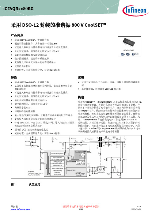
采用 DSO-12 封装的准谐振 800 V CoolSET ™产品亮点• 集成 800 V CoolMOS ™,雪崩能力强 • 创新型准谐振操作,其专有设计可降低 EMI• 可选进入和退出待机功率电平的增强型主动突发模式 • 主动突发模式,最低待机功率可小于 100 mW • 借助共源共栅配置实现快速启动 • 数字降频模式,提高整体系统效率 • 支持输入过压和欠压保护的可靠线路保护 • 完善的保护机制•无铅电镀、无卤模塑化合物,符合 RoHS 标准特性• 集成 800 V CoolMOS ™,雪崩能力强• 显著缩小高低压线路间的开关频率差,实现高效率和良好的 EMI 性能• 可选进入和退出待机功率电平的增强型主动突发模式 • 主动突发模式,最低待机功率可小于 100 mW • 借助共源共栅配置实现快速启动 • 数字降频技术,过零点可达 10 个 • 内置数字软启动 • 逐周期峰值电流限制• 最大导通/关断时间限制,以避免在启动和断电时产生噪音 • 支持输入过压和欠压保护的可靠线路保护•针对 VCC 过压、VCC 欠压、过载/开路、输入/输出过压及过温状况的自动重启模式保护• 受限的 VCC 短接至地的充电电流• 无铅电镀、无卤模塑化合物,符合 RoHS 标准应用• 适用于家用电器/白色家电、电视、电脑及服务器的辅助电源• 蓝光播放器、机顶盒和 LCD/LED 显示器描述准谐振 CoolSET ™ - (ICE5QRxx80BG) 是第五代准谐振集成电源 IC ,支持共源共栅配置,并针对离线开关模式电源进行了优化。
产品在单一封装中搭载了两个独立芯片,分别为控制器芯片和高压 MOSFET 芯片。
借助经改善的数字降频技术和专有的创新型准谐振操作,IC 可在实现低 EMI 效果时兼顾更高效率。
而增强型主动突发模式更是为待机功率范围的选择提供了灵活性。
此外, ICE5QRxx80BG 有宽的供电电压工作范围 (10.0~25.5 V), 功耗较低。
MP28275,DCDC降压芯片

TYPICAL APPLICATION (FOR NOTEBOOK)
Efficiency
VOUT=1.2V
1 IN BST 6
100
C4 0.1uF
90
EFFICIENCY (%)
L1 1.2uH
V IN=5V
C1 22uF 2, 3 SW 4, 5
80
VOUT 1.2V@5A R1 5K
70 60 50 40 30 20 10 0 0
1
MP28275 – 5A, 7V, SYNCHRONOUS STEP-DOWN CONVERTER WITH INTERNAL MOSFETS
ORDERING INFORMATION
Part Number* MP28275EL Package 3x4 QFN14 Top Marking MP28275 Free Air Temperature (TA) -20C to +85C
IN SW SW SW SW BST EN/SYNC EXPOSED PAD ON BACKSIDE
GND GND GND VCC NC PG FB
ABSOLUTE MAXIMUM RATINGS (1)
Supply Voltage VIN ......................................... 9V VSW ..........................-0.3V (-5V for<10ns) to 10V VBS ....................................................... VSW + 6V All Other Pins ..................................-0.3V to +6V Operating Temperature.............. -20C to +85C Continuous Power Dissipation (TA = +25°C) (2) ……………………………………………......2.6W Junction Temperature ...............................150C Lead Temperature ....................................260C Storage Temperature............... -65C to +15ommended Operating Conditions