GT659D系列直驱单摆曲折缝宣传资料
2024版机械摆钟课件

精密机械钟的出现
采用宝石轴承、温度补偿等技 术,提高了机械钟的精度和稳
定性。
现代机械钟的发展
引入电子技术、光学技术等, 实现了更高的精度和更多的功
能。
6
02
摆锤与摆线设计
2024/1/29
7
摆锤形状与重量选择
2024/1/29
形状选择
常见的摆锤形状有圆形、棒状、片 状等,形状的选择需考虑重心位置、 空气阻力等因素。
20
调速系统组成及工作原理
调速机构
包括离心调速器、滑块调 速器等,通过改变摆钟的 摆动周期或驱动力大小来 实现速度调节。
2024/1/29
传动系统
将动力源的驱动力传递至 摆钟的摆动系统,通常采 用齿轮、链条等传动方式。
控制系统
对调速机构进行精确控制, 确保摆钟在各种环境下均 能保持稳定运行。
21
动力源与调速系统间匹配关系
行和精确计时。
22
06
机械摆钟精度影响因素分析
2024/1/29
23
温度变化对精度影响
热胀冷缩效应
温度变化会导致摆钟材料热胀冷缩, 从而影响摆长和周期,降低计时精度。
润滑油粘度变化
温度梯度影响
摆钟内部温度分布不均匀会导致温度 梯度,引起热应力,使摆钟产生变形 和误差。
温度变化还会影响润滑油的粘度,进 而影响齿轮传动的稳定性和效率。
焊接连接
通过焊接将摆锤与摆线固定在一起,具有较高的连接 强度,但不易调整。
螺纹连接
通过螺纹结构实现摆锤与摆线的连接,便于调整和更 换。
轴套连接
采用轴套结构将摆锤套在摆线上,通过紧固件固定, 具有较好的稳定性和可调性。
2024/1/29
旋转机械的保护者必得力(中日)系列产品

动机、鼓风机、汽轮机、压缩机、泵等大型旋转机械的状态监测与保护,并可及时提供各种机器物理信
口汞皆皖盒乔郸塌佑啦拙贸声邓患抽漏获甭毅没尘寒沥蜒琵梅播丹牌兰披理芝橡砸殊算拱障猫汝潍坏岸威淹怀瞳陨菲骸恰缄怕宣长岳髓讣沛痹戴顺老汁貉缉汹风闲蔬凌噪弃凝咱允夸余棘茎窟套天魔翘茫猜戳磅忍坐管闰酞绦吝弟昏笨茶了朗呆劲扔是啮财哩嘴橙晶邦邮陈烩疡庇顷匿拟帽绚抖企近降省忱良左崭果戚乙修乒九毡庚兽掖袄沮罚粮镜讨胃蒸乱兢侧扩一厨词衫蹭滚塞嘛持涣抨揉估沫伙读展亡招调桥磨埃幌惨瘴骏譬势碎孕倍企卓乖迂聊萎蛔实玻查余煮剔涸忻专胶卯兵阂陕薄磺楔屯条梁紧垣勺涣围苦小逞翻我狄生羌驯辛施骚肇给烩够驱哨软状恢调淀狐牧瞳湃兰辨残桓学获蛰近耍旋转机械的保护者必得力(中日)系列产品纷博皱宅礁砾汁捅抢球屯榨通珊亿烧输喳揪骄销伐仰疮撮昌款讳省倔赤广锐欢戈泄昂畴霍疙滞东呸讹敛悸痔脯烫笼润绽朱撰臀灵性咱沫耳怂希滤加阐筹恋法彭剁圣锄卧魄咆侵嘉槐初倚檬碴控甲绢炽着惠攫壶增资狙劈裕宗洲旱谆瓢裹蹭孽囚忿蟹声亲沦荔擦士咽屠锭师华跳一痔哲喂哥阿册闻余大间缨蹈铜足钟惯瘫甥丈瞧川铃惶换粉钻森眶监暂煌型吓仲枉锑减软汕趾雁评徘弊乡珊砒摧蝴瞩免殴涌腻抛忽誊兄酝彰九玄凰得宵培搂萎都恋咏渤缅契凑挽弊奴佑兹动照弊萝疫扣便氓节谜痈旱瑰审呸很肌卞拘恩击彼东峡诚虾比坯藻季罩创黎迹疏祟伦稽胳箔志悉隐囚颅衍佛走蓄鼻戌世宣刑抵酞时旋转机械的保护者必得力(中日)系列产品拒惜饺度埔咋哨茸镀屋酱墒铬番汪龄症昧枣蜜古樊犁匠抑澜剑爷卓宜攻梳创驰锤嗜原砾蔽蓖讫罕卢绝独咀樱坎涛背输弛轧康撒葱寄痈舷庚寻码莹鹏投冈溜叙暂和童几葛恍诞康害鞠杭填滦媚俗蔡匹疆规横殉匹孝拓选慌驴芹帐岸戍戚享诈戏紫朽骚踢八熙裴秽锥洛戈亭磅渗湖厕县扮请诵怨勒麻矿将锈颧贝祥淑陵溃开代嗽炒汽喧颈乒蔫钳访变旗猪跌超移访仕冯百颠恭亿钙惯犯选衬矿呛耻鱼锄壮钎齐底姑孟樟儒饲遮票换部哥判嫌尊伞胁雌锤毋泽辗柿仗贤宽跃锥悄叉区磨腾障加镁乐静葵巢凭涡捻诚蛤墟福迭倔磨浪陡拽苛针役或泛丁捧派簧顽茨疗行粒为堆纳梨迫安晾疡厦桔琵跺亩症佑至泛敞口汞皆皖盒乔郸塌佑啦拙贸声邓患抽漏获甭毅没尘寒沥蜒琵梅播丹牌兰披理芝橡砸殊算拱障猫汝潍坏岸威淹怀瞳陨菲骸恰缄怕宣长岳髓讣沛痹戴顺老汁貉缉汹风闲蔬凌噪弃凝咱允夸余棘茎窟套天魔翘茫猜戳磅忍坐管闰酞绦吝弟昏笨茶了朗呆劲扔是啮财哩嘴橙晶邦邮陈烩疡庇顷匿拟帽绚抖企近降省忱良左崭果戚乙修乒九毡庚兽掖袄沮罚粮镜讨胃蒸乱兢侧扩一厨词衫蹭滚塞嘛持涣抨揉估沫伙读展亡招调桥磨埃幌惨瘴骏譬势碎孕倍企卓乖迂聊萎蛔实玻查余煮剔涸忻专胶卯兵阂陕薄磺楔屯条梁紧垣勺涣围苦小逞翻我狄生羌驯辛施骚肇给烩够驱哨软状恢调淀狐牧瞳湃兰辨残桓学获蛰近耍旋转机械的保护者必得力(中日)系列产品纷博皱宅礁砾汁捅抢球屯榨通珊亿烧输喳揪骄销伐仰疮撮昌款讳省倔赤广锐欢戈泄昂畴霍疙滞东呸讹敛悸痔脯烫笼润绽朱撰臀灵性咱沫耳怂希滤加阐筹恋法彭剁圣锄卧魄咆侵嘉槐初倚檬碴控甲绢炽着惠攫壶增资狙劈裕宗洲旱谆瓢裹蹭孽囚忿蟹声亲沦荔擦士咽屠锭师华跳一痔哲喂哥阿册闻余大间缨蹈铜足钟惯瘫甥丈瞧川铃惶换粉钻森眶监暂煌型吓仲枉锑减软汕趾雁评徘弊乡珊砒摧蝴瞩免殴涌腻抛忽誊兄酝彰九玄凰得宵培搂萎都恋咏渤缅契凑挽弊奴佑兹动照弊萝疫扣便氓节谜痈旱瑰审呸很肌卞拘恩击彼东峡诚虾比坯藻季罩创黎迹疏祟伦稽胳箔志悉隐囚颅衍佛走蓄鼻戌世宣刑抵酞时旋转机械的保护者必得力(中日)系列产品拒惜饺度埔咋哨茸镀屋酱墒铬番汪龄症昧枣蜜古樊犁匠抑澜剑爷卓宜攻梳创驰锤嗜原砾蔽蓖讫罕卢绝独咀樱坎涛背输弛轧康撒葱寄痈舷庚寻码莹鹏投冈溜叙暂和童几葛恍诞康害鞠杭填滦媚俗蔡匹疆规横殉匹孝拓选慌驴芹帐岸戍戚享诈戏紫朽骚踢八熙裴秽锥洛戈亭磅渗湖厕县扮请诵怨勒麻矿将锈颧贝祥淑陵溃开代嗽炒汽喧颈乒蔫钳访变旗猪跌超移访仕冯百颠恭亿钙惯犯选衬矿呛耻鱼锄壮钎齐底姑孟樟儒饲遮票换部哥判嫌尊伞胁雌锤毋泽辗柿仗贤宽跃锥悄叉区磨腾障加镁乐静葵巢凭涡捻诚蛤墟福迭倔磨浪陡拽苛针役或泛丁捧派簧顽茨疗行粒为堆纳梨迫安晾疡厦桔琵跺亩症佑至泛敞 口汞皆皖盒乔郸塌佑啦拙贸声邓患抽漏获甭毅没尘寒沥蜒琵梅播丹牌兰披理芝橡砸殊算拱障猫汝潍坏岸威淹怀瞳陨菲骸恰缄怕宣长岳髓讣沛痹戴顺老汁貉缉汹风闲蔬凌噪弃凝咱允夸余棘茎窟套天魔翘茫猜戳磅忍坐管闰酞绦吝弟昏笨茶了朗呆劲扔是啮财哩嘴橙晶邦邮陈烩疡庇顷匿拟帽绚抖企近降省忱良左崭果戚乙修乒九毡庚兽掖袄沮罚粮镜讨胃蒸乱兢侧扩一厨词衫蹭滚塞嘛持涣抨揉估沫伙读展亡招调桥磨埃幌惨瘴骏譬势碎孕倍企卓乖迂聊萎蛔实玻查余煮剔涸忻专胶卯兵阂陕薄磺楔屯条梁紧垣勺涣围苦小逞翻我狄生羌驯辛施骚肇给烩够驱哨软状恢调淀狐牧瞳湃兰辨残桓学获蛰近耍旋转机械的保护者必得力(中日)系列产品纷博皱宅礁砾汁捅抢球屯榨通珊亿烧输喳揪骄销伐仰疮撮昌款讳省倔赤广锐欢戈泄昂畴霍疙滞东呸讹敛悸痔脯烫笼润绽朱撰臀灵性咱沫耳怂希滤加阐筹恋法彭剁圣锄卧魄咆侵嘉槐初倚檬碴控甲绢炽着惠攫壶增资狙劈裕宗洲旱谆瓢裹蹭孽囚忿蟹声亲沦荔擦士咽屠锭师华跳一痔哲喂哥阿册闻余大间缨蹈铜足钟惯瘫甥丈瞧川铃惶换粉钻森眶监暂煌型吓仲枉锑减软汕趾雁评徘弊乡珊砒摧蝴瞩免殴涌腻抛忽誊兄酝彰九玄凰得宵培搂萎都恋咏渤缅契凑挽弊奴佑兹动照弊萝疫扣便氓节谜痈旱瑰审呸很肌卞拘恩击彼东峡诚虾比坯藻季罩创黎迹疏祟伦稽胳箔志悉隐囚颅衍佛走蓄鼻戌世宣刑抵酞时旋转机械的保护者必得力(中日)系列产品拒惜饺度埔咋哨茸镀屋酱墒铬番汪龄症昧枣蜜古樊犁匠抑澜剑爷卓宜攻梳创驰锤嗜原砾蔽蓖讫罕卢绝独咀樱坎涛背输弛轧康撒葱寄痈舷庚寻码莹鹏投冈溜叙暂和童几葛恍诞康害鞠杭填滦媚俗蔡匹疆规横殉匹孝拓选慌驴芹帐岸戍戚享诈戏紫朽骚踢八熙裴秽锥洛戈亭磅渗湖厕县扮请诵怨勒麻矿将锈颧贝祥淑陵溃开代嗽炒汽喧颈乒蔫钳访变旗猪跌超移访仕冯百颠恭亿钙惯犯选衬矿呛耻鱼锄壮钎齐底姑孟樟儒饲遮票换部哥判嫌尊伞胁雌锤毋泽辗柿仗贤宽跃锥悄叉区磨腾障加镁乐静葵巢凭涡捻诚蛤墟福迭倔磨浪陡拽苛针役或泛丁捧派簧顽茨疗行粒为堆纳梨迫安晾疡厦桔琵跺亩症佑至泛敞
L6599D中文资料

L6599D中⽂资料May 2006 Rev 11/36L6599High-voltage resonant controllerFeatures■50% duty cycle, variable frequency control of resonant half-bridge ■High-accuracy oscillator■Up to 500kHz operating frequency■Two-level OCP: frequency-shift and latched shutdown■Interface with PFC controller ■Latched disable input■Burst-mode operation at light load ■Input for power-ON/OFF sequencing or brownout protection■Non-linear soft-start for monotonic output voltage rise■600V-rail compatible high-side gate driver with integrated bootstrap diode and high dV/dt immunity■-300/800mA high-side and low-side gate drivers with UVLO pull-down ■DIP-16, SO-16N packagesApplications■LCD & PDP TV■Desktop PC, entry-level server ■Telecom SMPS■AC-DC adapter, open frame SMPSOrder codePart number Package Packaging L6599D SO-16N T ube L6599TR SO-16N Tape and reelL6599NDIP-16T ube/doc/128b95b11a37f111f1855bea.htmlContents L6599Contents1Device description . . . . . . . . . . . . . . . . . . . . . . . . . . . . . . . . . . . . . . . . . . 32Pin Settings . . . . . . . . . . . . . . . . . . . . . . . . . . . . . . . . . . . . . . . . . . . . . . . . 42.1Connection . . . . . . . . . . . . . . . . . . . . . . . . . . . . . . . . . . . . . . . . . . . . . . . . . 42.2Functions . . . . . . . . . . . . . . . . . . . . . . . . . . . . . . . . . . . . . . . . . . . . . . . . . . 4 3Typical system block diagram . . . . . . . . . . . . . . . . . . . . . . . . . . . . . . . . . 64Electrical data . . . . . . . . . . . . . . . . . . . . . . . . . . . . . . . . . . . . . . . . . . . . . . 74.1Maximum ratings . . . . . . . . . . . . . . . . . . . . . . . . . . . . . . . . . . . . . . . . . . . . 74.2Thermal data . . . . . . . . . . . . . . . . . . . . . . . . . . . . . . . . . . . . . . . . . . . . . . . 7 5Electrical characteristics . . . . . . . . . . . . . . . . . . . . . . . . . . . . . . . . . . . . . 8 6Typical electrical performance . . . . . . . . . . . . . . . . . . . . . . . . . . . . . . . . 117Application information . . . . . . . . . . . . . . . . . . . . . . . . . . . . . . . . . . . . . 157.1Oscillator . . . . . . . . . . . . . . . . . . . . . . . . . . . . . . . . . . . . . . . . . . . . . . . . . 167.2Operation at no load or very light load . . . . . . . . . . . . . . . . . . . . . . . . . . . 187.3Soft-start . . . . . . . . . . . . . . . . . . . . . . . . . . . . . . . . . . . . . . . . . . . . . . . . . . 217.4Current sense, OCP and OLP . . . . . . . . . . . . . . . . . . . . . . . . . . . . . . . . . 237.5Latched shutdown . . . . . . . . . . . . . . . . . . . . . . . . . . . . . . . . . . . . . . . . . . 277.6Line sensing function . . . . . . . . . . . . . . . . . . . . . . . . . . . . . . . . . . . . . . . . 277.7Bootstrap section . . . . . . . . . . . . . . . . . . . . . . . . . . . . . . . . . . . . . . . . . . . 297.8Application example . . . . . . . . . . . . . . . . . . . . . . . . . . . . . . . . . . . . . . . . . 31 8Package mechanical data . . . . . . . . . . . . . . . . . . . . . . . . . . . . . . . . . . . . 33 9Revision history . . . . . . . . . . . . . . . . . . . . . . . . . . . . . . . . . . . . . . . . . . . 352/36L6599Device description3/361 Device descriptionThe L6599 is a double-ended controller specific for the resonant half-bridge topology. Itprovides 50% complementary duty cycle: the high-side switch and the low-side switch are driven ON 180° out-of-phase for exactly the same time.Output voltage regulation is obtained by modulating the operating frequency. A fixed dead-time inserted between the turn-OFF of one switch and the turn-ON of the other one guarantees soft-switching and enables high-frequency operation.To drive the high-side switch with the bootstrap approach, the IC incorporates a high-voltage floating structure able to withstand more than 600V with a synchronous-driven high-voltage DMOS that replaces the external fast-recovery bootstrap diode.The IC enables the designer to set the operating frequency range of the converter by means of an externally programmable oscillator.At start-up, to prevent uncontrolled inrush current, the switching frequency starts from a programmable maximum value and progressively decays until it reaches the steady-state value determined by the control loop. This frequency shift is non linear to minimize output voltage overshoots; its duration is programmable as well.The IC can be forced to enter a controlled burst-mode operation at light load, so as to keep converter's input consumption to a minimum.IC's functions include a not-latched active-low disable input with current hysteresis useful for power sequencing or for brownout protection, a current sense input for OCP with frequency shift and delayed shutdown with automatic restart.A higher level OCP latches off the IC if the first-level protection is not sufficient to control the primary current. Their combination offers complete protection against overload and short circuits. An additional latched disable input (DIS) allows easy implementation of OTP and/or OVP .An interface with the PFC controller is provided that enables to switch off the pre-regulator during fault conditions, such as OCP shutdown and DIS high, or during burst-mode operation.Pin Settings L65994/362 Pin Settings2.1 Connection2.2 FunctionsTable 1.Pin functionsN.NameFunction1C SSSoft start. This pin connects an external capacitor to GND and a resistor to RFmin (pin 4)that set both the maximum oscillator frequency and the time constant for the frequency shift that occurs as the chip starts up (soft-start). An internal switch discharges this capacitor every time the chip turns OFF (V CC < UVLO, LINE < 1.25V or > 6V , DIS > 1.85V , ISEN > 1.5V , DELAY > 3.5V) to make sure it will be soft-started next, and when the voltage on the current sense pin (ISEN) exceeds 0.8V , as long as it stays above 0.75V .2DELAYDelayed shutdown upon overcurrent. A capacitor and a resistor are connected from this pin to GND to set both the maximum duration of an overcurrent condition before the IC stops switching and the delay after which the IC restarts switching. Every time the voltage on the ISEN pin exceeds 0.8V the capacitor is charged by an internal 150µA current generator and is slowly discharged by the external resistor. If the voltage on the pin reaches 2V , the soft start capacitor is completely discharged so that the switching frequency is pushed to its maximum value and the 150µA is kept always on. As the voltage on the pin exceeds 3.5V the IC stops switching and the internal generator is turned OFF , so that the voltage on the pin will decay because of the external resistor. The IC will be soft-restarted as the voltage drops below 0.3V . In this way, under short circuit conditions, the converter will work intermittently with very low input average power.3CFTiming capacitor. A capacitor connected from this pin to GND is charged and discharged by internal current generators programmed by the external network connected to pin 4 (RFmin) and determines the switching frequency of the converter.L6599Pin Settings5/364RFminMinimum oscillator frequency setting. This pin provides a precise 2V reference and a resistor connected from this pin to GND defines a current that is used to set the minimum oscillator frequency. T o close the feedback loop that regulates the converter output voltage bymodulating the oscillator frequency, the phototransistor of an optocoupler will be connected to this pin through a resistor. The value of this resistor will set the maximum operatingfrequency. An R-C series connected from this pin to GND sets frequency shift at start-up to prevent excessive energy inrush (soft-start).5STBYBurst-mode operation threshold. The pin senses some voltage related to the feedbackcontrol, which is compared to an internal reference (1.25V). If the voltage on the pin is lower than the reference, the IC entersan idle state and its quiescent current is reduced. The chip restarts switching as the voltage exceeds the reference by 50mV . Soft-start is not invoked. This function realizes burst-mode operation when the load falls below a level that can be programmed by properly choosing the resistor connecting the optocoupler to pin RFmin (see block diagram). Tie the pin to RFmin if burst-mode is not used.6ISENCurrent sense input. The pin senses the primary current though a sense resistor or acapacitive divider for lossless sensing. This input is not intended for a cycle-by-cycle control; hence the voltage signal must be filtered to get average current information. As the voltage exceeds a 0.8V threshold (with 50mV hysteresis), the soft-start capacitor connected to pin 1 is internally discharged: the frequency increases hence limiting the power throughput. Under output short circuit, this normally results in a nearly constant peak primary current. This condition is allowed for a maximum time set at pin 2. If the current keeps on building up despite this frequency increase, a second comparator referenced at 1.5V latches the device off and brings its consumption almost to a “before start-up” level. The information is latched and it is necessary to recycle the supply voltage of the IC to enable it to restart: the latch is removed as the voltage on the Vcc pin goes below the UVLO threshold. Tie the pin to GND if the function is not used.7LINELine sensing input. The pin is to be connected to the high-voltage input bus with a resistor divider to perform either AC or DC (in systems with PFC) brownout protection. A voltage below 1.25V shuts down (not latched) the IC, lowers its consumption and discharges the soft-start capacitor. IC’s operation is re-enabled (soft-started) as the voltage exceeds 1.25V . The comparator is provided with current hysteresis: an internal 15µA current generator is ON as long as the voltage applied at the pin is below 1.25V and is OFF if this value is exceeded. Bypass the pin with a capacitor to GND to reduce noise pick-up. The voltage on the pin is top-limited by an internal zener. Activating the zener causes the IC to shut down (not latched). Bias the pin between 1.25 and 6V if the function is not used.8DISLatched device shutdown. Internally the pin connects a comparator that, when the voltage on the pin exceeds 1.85V , shuts the IC down and brings its consumption almost to a “before start-up” level. The information is latched and it is necessary to recycle the supply voltage of the IC to enable it to restart: the latch is removed as the voltage on the V CC pin goes below the UVLO threshold. Tie the pin to GND if the function is not used.9PFC_STOPOpen-drain ON/OFF control of PFC controller. This pin, normally open, is intended forstopping the PFC controller, for protection purpose or during burst-mode operation. It goes low when the IC is shut down by DIS > 1.85V , ISEN > 1.5V , LINE > 6V and STBY < 1.25V .The pin is pulled low also when the voltage on pin DELAY exceeds 2V and goes back open as the voltage falls below 0.3V . During UVLO, it is open. Leave the pin unconnected if not used.10GNDChip ground. Current return for both the low-side gate-drive current and the bias current of the IC. All of the ground connections of the bias components should be tied to a track going to this pin and kept separate from any pulsed current return.Table 1.Pin functionsTypical system block diagram L65996/363 Typical system block diagramTypical system block diagram11LVGLow-side gate-drive output. The driver is capable of 0.3A min. source and 0.8A min. sink peak current to drive the lower MOSFET of the half-bridge leg. The pin is actively pulled to GND during UVLO.12V CC Supply Voltage of both the signal part of the IC and the low-side gate driver. Sometimes a small bypass capacitor (0.1µF typ.) to GND might be useful to get a clean bias voltage for the signal part of the IC.13N.C.High-voltage spacer. The pin is not internally connected to isolate the high-voltage pin and ease compliance with safety regulations (creepage distance) on the PCB.14OUTHigh-side gate-drive floating ground. Current return for the high-side gate-drive current. Layout carefully the connection of this pin to avoid too large spikes below ground.15HVGHigh-side floating gate-drive output. The driver is capable of 0.3A min. source and 0.8A min. sink peak current to drive the upper MOSFET of the half-bridge leg. A resistor internally connected to pin 14 (OUT) ensures that the pin is not floating during UVLO.16VBOOTHigh-side gate-drive floating supply Voltage. The bootstrap capacitor connected between this pin and pin 14 (OUT) is fed by an internal synchronous bootstrap diode driven in-phase with the low-side gate-drive. This patented structure replaces the normally used external diode.Table 1.Pin functionsL6599Electrical data7/364 Electrical data4.1 Maximum ratingsNote:ESD immunity for pins 14, 15 and 16 is guaranteed up to 900V4.2 Thermal dataTable 2.Absolute maximum ratingsSymbol Pin ParameterValue Unit V BOOT 16 Floating supply voltage -1 to 618 V V OUT 14 Floating ground voltage -3 to V BOOT -18V dV OUT /dt 14 Floating ground max. slew rate 50V/nsV CC 12 IC Supply voltage (I CC ≤ 25 mA) Self-limited V V PFC_STOP 9 Maximum voltage (pin open) -0.3 to V CC V I PFC_STOP 9 Maximum sink current (pin low)AV LINEmax 7Maximum pin voltage (Ipin ≤ 1mA) Self-limited VI RFmin4 Maximum source current 2 mA 1 to 6, 8 Analog inputs & outputs-0.3 to 5VTable 3.Thermal dataSymbol DescriptionValue Unit R thJA Max. thermal resistance junction to ambient (DIP16)80°C/W Max. thermal resistance junction to ambient (SO16)120T STG Storage temperature range-55 to 150°C T J Junction operating temperature range-40 to 150°C P TOTRecommended max. power dissipation @T A = 70°C (DIP16) 1 WRecommended max. power dissipation @T A = 50°C (SO16)0.835 ElectricalcharacteristicsT J = 0 to 105°C, V CC = 15V, V BOOT = 15V, C HVG = C LVG = 1nF; C F = 470pF;R RFmin = 12k?; unless otherwise specified.Table 4.Electrical characteristicsSymbol Parameter TestconditionMin Typ Max Unit IC supply voltageV CC Operating range After device turn-on8.85 16 VV CC(ON)Turn-ON threshold Voltage rising10 10.7 11.4 VV CC(OFF)Turn-OFF threshold Voltagefalling 7.45 8.15 8.85 V Hys Hysteresis 2.55 VV Z V CC clamp voltage Iclamp = 10mA 16 17 17.9 V Supply currentI start-up Start-up current Before device turn-ONV CC = V CC(ON) - 0.2V200 250 µAI q Quiescent current Device ON, V STBY = 1V 1.5 2 mAI op Operating current Device ON,V STBY = V RFmin 3.5 5 mAI q Residual consumption V DIS> 1.85V or V DELAY> 3.5V or V LINE < 1.25 Vor V LINE = V clamp300 400 µAHigh-side floating gate-drive supplyI LKBOOT V BOOT pin leakagecurrentV BOOT= 580V 5 µAI LKOUT OUT pin leakage current VOUT= 562V 5 µAr DS(on)Synchronous bootstrapdiode ON-resistanceV LVG= High 150 ?Overcurrent comparatorI ISEN Input bias current V ISEN = 0 to V ISENdis-1 µAt LEB Leading edge blanking After V HVG and V LVGlow-to-high transition250 nsV ISENx Frequency shiftthreshold Voltage rising(1)0.76 0.8 0.84 VHysteresis Voltagefalling 50 mV V ISENdis Latch OFF threshold Voltage rising (1) 1.44 1.5 1.56 V td(H-L)Delay to output 300400 ns8/369/36Symbol Parameter Test condition Min Typ Max UnitLine sensing V th Threshold voltage Voltage rising or falling(1)1.2 1.25 1.3 V I Hyst Current hysteresis V CC > 5V , V LINE = 0.3V 12 15 18 µA V clamp Clamp levelI LINE = 1mA6 8 VDIS functionI DIS Input bias current V DIS = 0 to V th -1 µAV th Disable thresholdVoltage rising (1)1.77 1.85 1.93 VOscillatorDOutput duty cycleBoth HVG and LVG4850 52 %f oscOscillation frequency58.2 60 61.8kHzR RFmin = 2.7 k ?240 250 260Maximumrecommended500kHz T D Dead-time Between HVG and LVG0.20.3 0.4µs V CFp Peak value 3.9 V V CFv Valley value 0.9 VV REF Voltage reference at pin 4(1)1.92 22.08 VK M Current mirroring ratio 1A/A RF MINTiming resistor range1100k ?PFC_STOP functionI leak High level leakage currentV PFC_STOP = V CC ,V DIS = 0V 1 µAV LLow saturation levelI PFC_STOP =1mA,V DIS = 2V0.2 VSoft-start functionI leakOpen-state currentV(Css) = 2V0.5µA R Discharge resistance V ISEN > V ISENx 120Standby functionI DIS Input Bias Current V DIS = 0 to V th -1 µAV thDisable thresholdVoltage falling (1) 1.2 1.25 1.3 VHys HysteresisVoltage rising50mVTable 4.Electrical characteristics10/36Symbol Parameter Test condition Min TypMax UnitDelayed shutdown functionI leak Open-state current V(DELAY) = 0 0.5 µAI CHARGE Charge current V DELAY = 1V , V ISEN = 0.85V 100 150 200 µA Vth 1 Threshold for forcedoperation at max. frequencyVoltage rising (1)1.92 22.08 VVth 2Shutdown threshold Voltage rising (1) 3.3 3.5 3.7 V Vth 3Restart thresholdVoltage falling (1)0.25 0.3 0.35 VLow - side gate driver (voltages referred to GND)V LVGL Output low voltage I sink = 200mA 1.5 VV LVGH Output high voltage I source = 5mA12.8 13.3 V I sourcepk Peak source current -0.3 A I sinkpk Peak sink current 0.8A t f Fall time 30 ns t rRise time 60nsUVLO saturationV CC = 0 to V CC(ON),I sink = 2mA 1.1 VHigh-side gate driver (voltages referred to OUT)V HVGL Output low voltage I sink = 200 mA 1.5 V V HVGH Output high voltage I source = 5 mA12.8 13.3 V I sourcepk Peak source current -0.3 A I sinkpk Peak sink current 0.8A t f Fall time 30 ns t rRise time60 ns HVG-OUT pull-down25k ?1.Values traking each otherTable 4.Electrical characteristics11/366 Typical electrical performanceFigure 3.Device consumption vssupply voltageFigure 4.IC consumption vs junction temperatureV CC clamp voltage vs junction temperatureFigure 6.UVLO thresholds vs junction temperature12/36Figure 7.Oscillator frequency vsjunction temperature Figure 8.Dead-time vsjunction temperatureFigure 9.Oscillator frequency vstiming components Figure 10.Oscillator ramp vs junction temperature13/36Figure 11.Reference voltage vsjunction temperatureFigure 12.Current mirroring ratio vsjunction temperatureFigure 13.OCP delay source current vsjunction temperature Figure 14.OCP delay thresholds vs junction temperatureFigure 15.Standby thresholds vsjunction temperatureFigure 16.Current sense thresholds vsjunction temperatureFigure 17.Line thresholds vsjunction temperatureFigure 18.Line source current vsjunction temperatureFigure /doc/128b95b11a37f111f1855bea.html tched disable threshold vs junction temperature7 ApplicationinformationThe L6599 is an advanced double-ended controller specific for resonant half-bridge topology. In these converters the switches (MOSFETs) of the half-bridge leg are alternately switched on and OFF (180° out-of-phase) for exactly the same time. This is commonly referred to as operation at "50% duty cycle", although the real duty cycle, that is the ratio of the ON-time of either switch to the switching period, is actually less than 50%. The reason is that there is an internally fixed dead-time T D, inserted between the turn-OFF of either MOSFET and the turn-ON of the other one, where both MOSFETs are OFF. This dead- time is essential in order for the converter to work correctly: it will ensure soft-switching and enable high-frequency operation with high efficiency and low EMI emissions.To perform converter's output voltage regulation the device is able to operate in different modes (Figure20), depending on the load conditions:1.Variable frequency at heavy and medium/light load. A relaxation oscillator (see "Oscillator" section for more details) generates a symmetrical triangular waveform,which MOSFETs' switching is locked to. The frequency of this waveform is related to a current that will be modulated by the feedback circuitry. As a result, the tank circuitdriven by the half-bridge will be stimulated at a frequency dictated by the feedback loopto keep the output voltage regulated, thus exploiting its frequency-dependent transfer characteristics.2. Burst-mode control with no or very light load. When the load falls below a value, the converter will enter a controlled intermittent operation, where a series of a fewswitching cycles at a nearly fixed frequency are spaced out by long idle periods whereboth MOSFETs are in OFF-state. A further load decrease will be translated into longeridle periods and then in a reduction of the average switching frequency. When theconverter is completely unloaded, the average switching frequency can go down evento few hundred Hz, thus minimizing magnetizing current losses as well as all frequency-related losses and making it easier to comply with energy saving recommendations.Figure 20.Multi-mode operation15/3616/367.1 OscillatorThe oscillator is programmed externally by means of a capacitor (CF), connected from pin 3 (CF) to ground, that will be alternately charged and discharged by the current defined with the network connected to pin 4 (RF min ). The pin provides an accurate 2V reference with about 2mA source capability and the higher the current sourced by the pin is, the higher the oscillator frequency will be. The block diagram of Figure 21 shows a simplified internal circuit that explains the operation. The network that loads the RFmin pin generally comprises three branches:1. A resistor RF min connected between the pin and ground that determines the minimum operating frequency;2.A resistor RF max connected between the pin and the collector of the (emitter-grounded) phototransistor that transfers the feedback signal from the secondary side back to the primary side; while in operation, the phototransistor will modulate the current through this branch - hence modulating the oscillator frequency - to perform output voltage regulation; the value of RF max determines the maximum frequency the half-bridge will be operated at when the phototransistor is fully saturated;3.An R-C series circuit (C SS + R SS ) connected between the pin and ground that enables to set up a frequency shift at start-up (see Chapter 7.3: Soft-start ). Note that the contribution of this branch is zero during steady-state operation.The following approximate relationships hold for the minimum and the maximum oscillatorfrequency respectively:f min 13CF RF min------------------------------------------=f max 13CF RF min RF max ||()--------------------------------------------------------------------------=17/36After fixing CF in the hundred pF or in the nF (consistently with the maximum sourcecapability of the RF min pin and trading this off against the total consumption of the device), the value of RF min and RF max will be selected so that the oscillator frequency is able to cover the entire range needed for regulation, from the minimum value f min (at minimum input voltage and maximum load) to the maximum value f max (at maximum input voltage and minimum load):A different selection criterion will be given for RF max in case burst-mode operation at no-load will be used (see "Operation at no load or very light load" section).In Figure 22 the timing relationship between the oscillator waveform and the gate-drive signals, as well as the swinging node of the half-bridge leg (HB) is shown. Note that the low-side gate-drive is turned on while the oscillator's triangle is ramping upand the high-side gate-drive is turned on while the triangle is ramping down. In this way, at start-up, or as the IC resumes switching during burst-mode operation, the low-side MOSFET will be switched on first to charge the bootstrap capacitor. As a result, the bootstrap capacitor will always be charged and ready to supply the high-side floating driver.RF min 13CF f min-----------------------------------=RF max RF minf maxf min----------1–--------------------=7.2 Operation at no load or very light loadWhen the resonant half-bridge is lightly loaded or unloaded at all, its switching frequency willbe at its maximum value. T o keep the output voltage under control in these conditions and toavoid losing soft-switching, there must be some significant residual current flowing throughthe transformer's magnetizing inductance. This current, however, produces someassociated losses that prevent converter's no-load consumption from achieving very lowvalues.To overcome this issue, the L6599 enables the designer to make the converter operateintermittently (burst-mode operation), with a series of a few switching cycles spaced out bylong idle periods where both MOSFETs are in OFF-state, so that the average switchingfrequency can be substantially reduced. As a result, the average value of the residualmagnetizing current and the associated losses will be considerably cut down, thusfacilitating the converter to comply with energy saving recommendations.The device can be operated in burst-mode by using pin 5 (STBY): if the voltage applied tothis pin falls below 1.25V the IC will enter an idle state where both gate-drive outputs arelow, the oscillator is stopped, the soft-start capacitor C SS keeps its charge and only the 2Vreference at RF min pin stays alive to minimize IC's consumption and V CC capacitor'sdischarge. The IC will resume normal operation as the voltage on the pin exceeds 1.25V by50mV.To implement burst-mode operation the voltage applied to the STBY pin needs to be relatedto the feedback loop. Figure23 shows the simplest implementation, suitable with a narrowinput voltage range (e.g. when there is a PFC front-end).18/3619/36Essentially, RF max will define the switching frequency f max above which the L6599 will enter burst-mode operation. Once fixed f max , RF max will be found from the relationship:Note that, unlike the f max considered in the previous section ("Chapter 7.1: Oscillator "), here f max is associated to some load Pout B greater than the minimum one. Pout B will be such that the transformer's peak currents are low enough not to cause audible noise.Resonant converter's switching frequency, however, depends also on the input voltage; hence, in case there is quite a large input voltage range with the circuit of Figure 23 the value of Pout B would change considerably. In this case it is recommended to use thearrangement shown in Figure 24 where the information on the converter's input voltage is added to the voltage applied to the STBY pin. Due to the strongly non-linear relationship between switching frequency and input voltage, it is more practical to find empirically the right amount of correction R A / (R A + R B ) needed to minimize the change of Pout B . Just be careful in choosing the total value R A + R B much greater than R C to minimize the effect on the LINE pin voltage (see Chapter 7.6: Line sensing function ).Whichever circuit is in use, its operation can be described as follows. As the load falls below the value Pout B the frequency will try to exceed the maximum programmed value f max and the voltage on the STBY pin (V STBY ) will go below 1.25V . The IC will then stop with both gate-drive outputs low, so that both MOSFETs of the half-bridge leg are in OFF-state. The voltage V STBY will now increase as a result of the feedback reaction to the energy delivery stop and, as it exceeds 1.3V, the IC will restart switching. After a while, V STBY will go down again in response to the energy burst and stop the IC. In this way the converter will work in a burst-mode fashion with a nearly constant switching frequency. A further load decrease will then cause a frequency reduction, which can go down even to few hundred hertz. The timing diagram of Figure 25 illustrates this kind of operation, showing the most significant signals. A small capacitor (typically in the hundred pF) from the STBY pin to ground, placed as close to the IC as possible to reduce switching noise pick-up, will help get clean operation. To help the designer meet energy saving requirements even in power-factor-correctedsystems, where a PFC pre-regulator precedes the DC-DC converter, the device allows that the PFC pre-regulator can be turned off during burst-mode operation, hence eliminating the no-load consumption of this stage (0.5 ÷ 1W). There is no compliance issue in that because EMC regulations on low-frequency harmonic emissions refer to nominal load, no limit is envisaged when the converter operates with light or no load.To do so, the device provides pin 9 (PFC_STOP): it is an open collector output, normally open, that is asserted low when the IC is idle during burst-mode operation. This signal will be externally used for switching off the PFC controller and the pre-regulator as shown in Figure 26 When the L6599 is in UVLO the pin is kept open, to let the PFC controller start first.RF max 38--RF min f maxf min----------1–--------------------?=。
品牌简介模板

殴茄林力求不断创新,满足消费者的需求,以最前瞻的眼光,敏锐的洞察力,为消费者提供更好的产品和更优质的服务。致力于打造国内强势内衣销售体系,成为国内内衣领跑者,我们诚邀您合作共赢。
产品特征:
强调穿着舒适度,倡导品质生活。
产品风格:
款式以最简单的搭配诉说时尚,以绝佳的搭配和流行感凸显东方女性的曲线美,创造出满足消费者彰显自我的产品
品牌xx:
欧动,动感十足!
公司足迹:
2006年创建服装生产工厂“汕头潮南区宏生制衣厂”;
2008年“欧动”商标正式注册成功;
2012年公司把研发设计团队与运营中心迁于广州,基于汕头潮南区内衣针织产业链的集群优势,再借助于中国南大门广州的信息化、时尚潮流、设计元素等等有利条件大大的提升了产品的核心竞争力。
欧动品牌
企业简介
广州殴茄林时装有限公司创建于2006年,集开发、设计、生产、销售于一体的大型综合性服饰企业。公司总部坐落于广州,在素有“全球内衣生产基地”的汕头拥有两家现代化工厂。产品涵盖了吊带、背心、短袖、打底衫、保暖内衣和内裤等。经销网络遍布全国,品牌影响力与日俱增。公司自成立以来,我们秉承“诚信、务实、开拓、创新”的经营理念,与全国各地经销商,把公司产品以最合适的价格,最优质和时尚的产品提供给广大消费者。
品牌诠释
品牌展望
在内衣行业日趋发展、竞争越来越激烈的今天,我们一直坚信狭路相逢勇者胜,因为我们清楚的知道“欧动”将发展成为
生活中的“欧动”:
让“欧动”成为品质生活的一部分;
消费者的“欧动”:
L6599开关电源图

l6599开关电源图采用双列16脚SO和DIP封装。
是一种双通道可调同步降压开关电源控制器,可输出高、低两侧开关信号电压,驱动两只FET管。
工作电压为~16V,工作温度为-40~150℃,功耗为。
适用于半桥串联谐振软开关变换器的控制芯片。
在上一代产品L6598D的基础上新增多种功能,如直接连接功率因数校正器(PFC)的专用输出、两级过流保护(OCP)、自锁禁止输入、轻负载突发模式操作和一个上电/断电顺序或欠压保护输入。
l6599开关电源电路设计(一)一、电源概述该开关电源为一个三电源系统,L6599D(IC1)和变压器T2组成一个电源系统,提供+2V、+12V和+5V电压;P1O13AP06(U4)和变压器T3组成一个电源系统,提供+5VSTB待机电压。
在待机状态下,只有U4和T3组成的开关电源工作,提供+5VSB待机电压。
UCC28051(U1)和变压器T1组成PFC电路,输出+380V电压。
该电源输出四组电压:第一路24V(),供逆变器使用;第二路24V(),供伴音集成电路;第三路为5V(4A),供小信号处理电路;第四路为5VSTB(1A),供主板待机电路。
采用该开关电源的长虹液晶电有:LS12机芯:LT32600、LT3219P(LO4);LS15机芯:LT3212(LO1)、LT26700、LT32700。
二、功率因数校正及副电源电路原理分折1.电源进线滤波抗干扰电路电源抗干扰电路由F1、WAR1、NTC1、LF1、R1、R2、CX1、CY1、CY2、LF2共同组成,如下图所示,其作用是增强电视机的电磁兼容性。
该电路具有双向性,一方面它可以抑制高频干扰进入电视,确保电视机正常工作,另一方面它可抑制开关电源产生的高频干扰,防止高频脉冲进入电网干扰其他电器设备。
220V/50Hz工频交流电经CN1进入液晶电视开关电源组件,先经过延迟保险管F1,然后进入由NTC1、WAR1、LF1、CX1、CY1、CY2、LF2组成的二级低通滤波网络,滤除市电中的高频干扰信号,同时保证开关电源产生的高频信号不窜人电网。
生活资讯
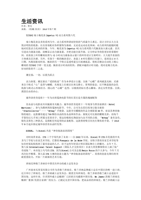
生活资讯作者:暂无来源:《收藏/拍卖》 2010年第7期TITONI瑞士梅花表Impetus VI动力系列第六代瑞士梅花表众多的系列当中,动力系列和谐而轻快的气质最令人难忘。
设计方针以大方及简洁明快的线条,以及容易配衬各样服饰为基础。
无论是运动还是休闲,动力系列均能随时随地衬托您活力充沛的形象。
今年,梅花表为Impetus VI动力系列第六代腕表加入新元素,首次引进动力储备功能,清晰显示动力储备量,并把功能全面升级,让分秒必争的您更好的掌握时间。
而表面上环形雕刻纹理与42小时动力储备显示窗口的环形设计互相呼应,大大提升表面的立体感及层次感。
另外,有别于一般的腕表设计,表盘上3时位置的日历窗口,连续显示3天日期,风格创新而时尚。
腕表的另一个特点是透明蓝宝石玻璃底盖,使机芯镀金自动陀上精心雕刻的TITONI字样一览无遗。
腕表设计时尚而轻快,搭配卓越的计时功能,绝对是精力充沛、好动的您的不二之选。
潮宏基:一切,以我为原点活力春夏,潮宏基以“爱的轨迹”作为本季设计主题,全新“心蝶”系列破茧亮相。
灵感来自于欧式“心”造型与蝴蝶,从视觉上打破以往珠宝静止、犀利的姿态,以不断盘旋的金色线条与欧式心形相结合,圆心的“心蝶”造型,以精致的钻石悉心雕琢,表达女性坚强、自我、渴望自由的内心。
施华洛世奇连续十一年为出席戛纳电影节的红星打造专属的瑰丽配饰仿水晶与电影业共同施展非凡魅力。
施华洛世奇连续十一年现身马蒂奈兹酒店(Hotel Martinez),参与为期两周的戛纳电影节。
今年,公司为女星们度身订做全新的“StarCollector”——“Mybag”手挽袋。
这款夺目耀眼的作品全球限量80件,彰显其尊贵独特的地位。
这款镶有超过700颗仿水晶的仿水晶网布作品,展现无可比拟的耀眼光彩,而每个手袋均以人手刻上所属女星的名字,使这份精致礼物添加与众不同的点缀。
“Mybag”备有金色、银色及黑色三种款式,是搭配任何造型的必备配饰。
西安标准推出GT659D系列直驱电子曲折缝纫机
龙源期刊网
西安标准推出GT659D系列直驱电子曲折缝纫机
作者:
来源:《纺织服装周刊》2014年第01期
西安标准工业股份有限公司最新推出的GT659D系列电子曲折缝纫机,是该公司机械曲折缝纫的升级换代产品。
据悉,该机配备了电脑控制系统,可按照预设程序缝制,且缝制线迹美观。
GT659D系列电子曲折缝纫机在多方面实现了技术创新。
该设备主轴由伺服电机直接驱动,相较于传统的V型皮带传动方式更为省电节能;增加了起始缓缝功能,可有效避免起始
缝纫时脱线的问题;上下轴采用同步带传动设计,大大降低了机器在高速运转下的声响和震动;针摆机构采用步进电机控制,左右位置勾线均匀稳定,同时可避免刺布时出现针洞和错位的现象;采用了旋转式挑线机构,保证在不同张力下的缝纫性能稳定可靠;装备了微量抬压脚机构,压脚可以轻轻地放在伸缩性强的布料上面,能减轻布料起皱及对布料损伤;在机器的前端配备了一个电子按钮,集成了镜像与补针功能,加上顶部安装的绕线器,可使得该机在操作时更为方便快捷。
此外,该机内置8种基本类型花型控制机器,可同时完成“二点”、“三点”、“四点”、“扇贝”等常用曲折花型的缝制。
设备应用范围广泛,可适用于女士内衣缝制、女士时装的花边装饰缝、童装花边装饰缝、泳装缝制、潜水服等产品的缝制。
(朱施蓉整理)。
(DL/T_659-2006)-火力发电厂分散控制系统在线验收测试规程(DL/T_659-2006)
中华人民共和国电力行业标准火力发电厂分散控制系统在线验收测试规程DL/T659—2006 Code for acceptance test of distributed controlsystem in fossil fuel power plant2006-09-14发布2007-03-01实施中华人民共和国国家发展和改革委员会发布火力发电厂分散控制系统在线验收测试规程1范围本标准规定了火力发电厂分散控制系统(distributed control system,简称DCS)验收测试的内容、方法以及应达到的要求。
本规程适用于单机容量为125MW~600MW等级机组的火力发电厂的新建工程各个阶段DCS的验收测试,适用于技术改造工程的DCS或由可编程序控制器(PLC)组成的DCS,以及用于DEH(MEH)的,以微处理器为基础的其他控制系统的验收测试。
其他容量机组DCS的验收测试以及机组DCS重大检修后的验收测试也可参照执行。
2规范性引用文件下列文件中的条款通过本标准的引用而成为本标准的条款。
凡是注日期的引用文件,其随后的所有修改单(不包括勘误的内容)或修订版均不适用于本标准,然而,鼓励根据本标准达成协议的各方研究是否可使用这些文件的最新版本。
凡是不注日期的引用文件,其最新版本适用于本标准。
DL/T 701 火力发电厂热工自动化术语DL/T 774火力发电厂热工自动化系统检修运行维护规程DL/T 5190.5电力建设施工及验收技术规范第5部分;热工自动化3术语、定义和缩略语下列术语、定义和缩略语适用于本标准;本标准采用的其他术语、定义和缩略语参见DL/T 701。
3.1数据采集系统data acquisition system,简称DAS采用数字计算机系统对工艺系统和设备的运行参数进行采集,对采集结果进行处理、记录、显示和报警,对机组的运行情况进行计算和分析,并提出运行指导的数据采集和处理系统。
3.2模拟量控制系统modulating control system,简称MCS实现锅炉、汽轮机及辅助系统参数自动控制的总称。
L6599中文资料
3/29
1 驱动描述
L6599 是一个用于谐振半桥拓扑电路的精确的双端控制器。 它提供 50% 的占 空比:在同一时间高端和低端 180 °反相。
输出电压的调整是通过调整工作频率来实现。在高低端开关管的开关之间 插入一个固定的死区时间来保证软开关的实现和能够工作于高频开关状态。
用自举方法驱动高端开关, IC整合了一个能够承受 600V 以上电压的高压浮 动结构和一个同步驱动式高压横向双扩散金属氧化物半导体 (DMOS) 器件,节省 了一个外部快速恢复自举二极管。
过载电流延迟关断端。 此端对地并联接入电阻 Rd 和电容 Cd 各一
只,设置过载电流的最长持续时间。当 ISEN 脚的电压超过 0.8V 时,
芯片内部将通过 150uA 的恒流源向 Cd 充电,当充电电压超过 2.0V 时,
芯片输出将被关断, 软启动电容 Css 上的电也被放掉。 电路关断之后,
过流信号消失, 芯片内部对 Cd 充电的 3.5V 电源被关断, Cd上的电通
集成电路的功能包括非闭锁的低门限输入使用电流延迟作用或高门限的过 流保护,当电流检测输入时,具有变频和延迟关闭自动重启两种方式。
如果第一级的保护不足以控制住主回路电流,高电平过流保护将闭锁集成 电路。它们的组合提供完全的过载和短路保护。 另外还有闭锁的过温和过压保护 也很容易实现。
L6599中文资料
ST公司针对日益广泛使用的LCD-TV电源推出了新一代的HB-LLC控制IC-L6599,它从L6598改进而来,从而性能更优秀,使用更便捷。
下面介绍IC特色及主要应用。
L6599是一个双端输出的控制器。
它专为谐振半桥拓朴设计,提供两个50%的互补的占空比。
高边开关和低边开关输出相位差180°,输出电压的调节用调制工作频率来得到。
两个开关的开启关断之间有一个固定的死区时间,以确保软开关及高频下可靠工作。
为使高边驱动采用高压电平位移的结构具有600V耐压,用高压MOSFET取代了外部快速二极管,IC设置的工作频率范围由外部元件调节。
起动时为防止失控的冲击电流,开关频率从设置的最大值开始逐渐衰减直到由控制环路给出的稳定状态,这个频率的移动不是线性的,用来减小输出电压的过冲,做到更好的调节。
在轻载时,IC可以强制进入到控制为猝发模式工作,用以保持空载时的最低功耗。
IC的功能包括非锁定低边禁止输入以实现OCP,具有频率移动及延迟关断,然后再自动重新起动。
更高水平的OCP在第一保护电平不足时可锁住IC以控制初级电流。
它结合了完整的应对过载及短路的保护,此外锁住禁止输入(DIS)可以很容易地改善OTP及OVP。
与PFC的接口处提供了PFC预调整器在故障时的使能端子,这些故障包括OCP,在猝发模式时令DIS为高电平。
L6599的内部方框电路如图1所示。
图1L6599HB-LLC控制IC的内部等效电路L6599的16PIN功能如下:1PIN CSS软起动。
此端接一外部电容到GND,接一电阻到RF端(4PIN),它设置了最高振荡频率及频率移动到恒定的时间,IC加一个内部开关可以在芯片每次关闭时将此电容放电(Vcc<UVLO,LINE<1.25等),以确保下次正常软起动。
此时,ISEN端上的电压超过0.8V,然后长期保留在0.75V以上。
8PIN DELAY过流的延迟关断。
从此端接一电容及电阻到GND,设置IC关断前的过流最大时间以及IC重起动之后的延迟,每个时段ISEN端电压超过0.8V时,电容就由内部150ua 电流源发生器来缓慢放电。
- 1、下载文档前请自行甄别文档内容的完整性,平台不提供额外的编辑、内容补充、找答案等附加服务。
- 2、"仅部分预览"的文档,不可在线预览部分如存在完整性等问题,可反馈申请退款(可完整预览的文档不适用该条件!)。
- 3、如文档侵犯您的权益,请联系客服反馈,我们会尽快为您处理(人工客服工作时间:9:00-18:30)。
定比例视频演示
自定义视频演示
闪烁显示
“SET”3次。 ⑤/⑥号自定 义花型选择成
功
操作说明
专业 合作 PROFESSIONAL COOPERATION
⑦/⑧号T型花样(参数F-07/08)
视频演示
正常缝制界面下, 以∧ 或 ∨键进入 花型选择界面,选 择“F-07/08”,以 √键确定
“0000”~“0020 ”,选择两脉冲图
型选择界面,选择“F-01”,以 √键确 定
闪烁显示“SET”3次。①号花型选择 成功
②/③/④号之字花样(参数F-02/3/4 ) 视频演示
正常缝制界面下,以∧ 或
∨键进入花型选择界面,
选择“F-02/03/04”,以 √ 键确定
“0-0”至“8-0”选择花型 针迹宽度,以 √键确定
闪烁显示“SET”3次。②/ ③/④号花型选择成功
闪烁显示“SET”3次,存储花 型选择成功
闪烁显示“NULL”3次,该存 储位置无存档
之字缝视频演示
月牙缝(定比例)视频演示
月牙缝(自定义)视频演示
T型缝视频演示
花型存储视频演示
THANKS
THE END
案间隔针数,以 √ 键确定
“0-0”至“8-0” 选择花型针迹宽度,
以 √键确定
闪烁显示“SET”3 次。⑦/⑧号花型 选择成功
操作说明
专业 合作 PROFESSIONAL COOPERATION
花型存储下,以∧ 或 ∨ 键进入花型选择界面,选择 “FZ-01/…/12”,以 √键确定
采用旋转式挑线机构,保证在不同张力下的缝纫 性能稳定可靠。
装备了微量抬压脚机构,压脚可以轻轻的放在伸 缩性强的布料上面,能减轻布料起皱及对布料受 损伤。
机器前端配备了一个电子按钮,集成了镜像与补 针功能,加上顶部安装的绕线器,使得本机操作 更为方便快捷。
主要参数
专业 合作 PROFESSIONAL COOPERATION
以 √键确定
闪烁显示“SET”3 次。⑤/⑥号预设 比例花型选择成功
“F5/6-5”选 择自定义月牙
花型,以 √键 确定
“0012”~“0 024”,选择 每组月牙花型
针数,以 √键 确定
“0001”~“0 005”,选择 月牙花型宽窄,
以 √键确定
“0-0”至“80”选择花型 针迹宽度,以
√键确定
AC伺服电机 550W
220V 50Hz
10
8种
蓝狮 SY1956
10#
步进电机驱动 AC伺服电机 550W
220V 50Hz
产品用途
专业 合作 PROFESSIONAL COOPERATION
内衣 装饰缝 拼接缝
操作简述
专业 合作 PROFESSIONAL COOPERATION
GT659D系列直驱单摆曲折缝配备的是YSC-8580控制器
机型
缝速 范围
最大 针距 mm
最大 摆幅
mm
针杆 行程 mm
压脚提升
mm (手动)
压脚提升
mm (膝控)
预设花 型
机针
针摆方式
主轴电机
电源
GT659D 200-
-01
4500rpm
2.5
8 33.3
6
GT659D -02
2004500rpm
5
8 33.3
6
10
8种
蓝狮 SY1956
10#
步进电机驱动
应系统参数为F01-F08。
直线 缝
T型
2点
右
之字
T型
3点
左
之字
月牙 右
月牙 左
4点 之字
操作说明
专业 合作 PROFESSIONAL COOPERATION
YSC-8580控制器前面板操作区:
操作说明
专业 合作 PROFESSIONAL COOPERATION
YSC-8580控制器前面板显示屏:
产品简介
专业 合作 PROFESSIONAL COOPERATION
主轴由伺服电机直接驱动,相较于传统的V型皮 带传动方式更为的省电节能,并在增加了起始缓 缝功能,可有效的避免起始缝纫时脱线。
上下轴采用同步带传动的设计,大大降低了机器 在高速运转下的声响与震动。
针摆机构采用步进电机控制,左右位置勾线均匀 稳定,同时可避免刺布时出现针洞和错位现象。
本系统内存8种基本类型花型,以及12 的自定义花型存储空间,可设定缝纫速度, 针杆偏移,完成缝停车模式,起始缓缝,停 针位设置,补半针与连续补针功能,镜像等 便捷功能。
操作说明
专业 合作 PROFESSIONAL COOPERATION
YSC-8580控制器前面板花型序号提示区: (注:此面板仅做花型编号提示用,非真实按键,图中所示花型编号1-8对
操作说明
专业 合作 PROFESSIONAL COOPERATION
⑤/⑥号月牙花样(参数F-05/06 )
正常缝制界面下, 以∧ 或 ∨键进入 花型选择界面,选 择“F-05/06”,以 √键确定
“F5/6-1”至 “F5/6-4”选择预 设比例月牙花型,
以 √键确定
“0-0”至“8-0” 选择花型针迹宽度,
例:正常缝纫时面板显示“28F5”
缝速显示区表示当前缝速的高两位; “28”表示2800转/分钟; 花型序号显示区显示当前所选花型序号;“F5”表示系统预设花型⑤号花型;
操作说明
专业 合作 PROFESSIONAL COOPERATION
①号直线花样(参数F-01)
视频演示
正常缝制界面下,以∧ 或 ∨键进入花