MAX485_486
MEMORY存储芯片MAX485EEPA+中文规格书
Low-Power, Slew-Rate-Limited RS-485/RS-422 Transceivers2MAX481/MAX483/MAX485/MAX487–MAX491/MAX1487ABSOLUTE MAXIMUM RATINGSSupply Voltage (V CC ) (12V)Control Input Voltage (RE , DE)...................-0.5V to (V CC + 0.5V)Driver Input Voltage (DI).............................-0.5V to (V CC + 0.5V)Driver Output Voltage (A, B)...................................-8V to +12.5VReceiver Input Voltage (A, B).................................-8V to +12.5VReceiver Output Voltage (RO)....................-0.5V to (V CC + 0.5V)Continuous Power Dissipation (T A = +70°C)8-Pin Plastic DIP (derate 9.09mW/°C above +70°C)....727mW14-Pin Plastic DIP (derate 10.00mW/°C above +70°C)..800mW8-Pin SO (derate 5.88mW/°C above +70°C).................471mW 14-Pin SO (derate 8.33mW/°C above +70°C)...............667mW 8-Pin µMAX (derate 4.1mW/°C above +70°C)..............830mW 8-Pin CERDIP (derate 8.00mW/°C above +70°C).........640mW 14-Pin CERDIP (derate 9.09mW/°C above +70°C).......727mW Operating Temperature Ranges MAX4_ _C_ _/MAX1487C_ A...............................0°C to +70°C MAX4__E_ _/MAX1487E_ A.............................-40°C to +85°C MAX4__M_/MAX1487MJA.............................-55°C to +125°C Storage Temperature Range.............................-65°C to +160°C Lead Temperature (soldering, 10sec).............................+300°C DC ELECTRICAL CHARACTERISTICS(V CC = 5V ±5%, T A = T MIN to T MAX , unless otherwise noted.) (Notes 1, 2)Stresses beyond those listed under “Absolute Maximum Ratings” may cause permanent damage to the device. These are stress ratings only, and functional operation of the device at these or any other conditions beyond those indicated in the operational sections of the specifications is not implied. Exposure to absolute maximum rating conditions for extended periods may affect device reliability.V V IN = -7V V IN = 12V V IN = -7V V IN = 12V Input Current (A, B)I IN2V TH k Ω48-7V ≤V CM ≤12V, MAX487/MAX1487R INReceiver Input Resistance -7V ≤V CM ≤12V, all devices exceptMAX487/MAX1487R = 27Ω(RS-485), Figure 40.4V ≤V O ≤2.4VR = 50Ω(RS-422)I O = 4mA, V ID = -200mV I O = -4mA, V ID = 200mV V CM = 0V -7V ≤V CM ≤12V DE, DI, REDE, DI, RE MAX487/MAX1487,DE = 0V, V CC = 0V or 5.25VDE, DI, RE R = 27Ωor 50Ω, Figure 4R = 27Ωor 50Ω, Figure 4R = 27Ωor 50Ω, Figure 4DE = 0V;V CC = 0V or 5.25V,all devices exceptMAX487/MAX1487CONDITIONS k Ω12µA ±1I OZR Three-State (high impedance)Output Current at Receiver V 0.4V OL Receiver Output Low Voltage3.5V OH Receiver Output High VoltagemV 70ΔV TH Receiver Input HysteresisV -0.20.2Receiver Differential ThresholdVoltage-0.2mA 0.25mA -0.81.01.55V OD2Differential Driver Output(with load)V 2V 5V OD1Differential Driver Output (no load)µA ±2I IN1Input Current V 0.8V IL Input Low VoltageV 2.0V IH Input High VoltageV 0.2ΔV OD Change in Magnitude of DriverCommon-Mode Output Voltagefor Complementary Output StatesV 0.2ΔV OD Change in Magnitude of DriverDifferential Output Voltage forComplementary Output StatesV 3V OC Driver Common-Mode OutputVoltageUNITS MIN TYP MAX SYMBOL PARAMETERLow-Power, Slew-Rate-Limited RS-485/RS-422 Transceivers7MAX481/MAX483/MAX485/MAX487–MAX491/MAX1487______________________________________________________________Pin DescriptionFigure 1. MAX481/MAX483/MAX485/MAX487/MAX1487 Pin Configuration and Typical Operating Circuit。
max485芯片
max485芯片MAX485是一种用于串行通讯的芯片,它可以实现半双工的通信,常用于RS-485网络中。
这款芯片具有低功耗、高速率、低电压、可靠性高等特点,被广泛应用于工业自动化、远程监控、数据采集等领域。
MAX485芯片采用了双绞四线制接口,可以实现长距离传输,通信距离可达1200米。
其通信速率可以高达2.5Mbps,同时还支持多点连接,可以连接最多32个驱动器和接收器。
MAX485芯片的工作电压范围为3.0V至5.25V,因此可以适应不同的工作环境。
在低功耗模式下,它的供电电流仅为1μA,非常适合电池供电的应用。
此外,MAX485还具有过温保护功能,可以保护芯片免受过热损坏。
MAX485芯片的架构采用了低功耗CMOS技术,具有自动接收释放和禁用保护电路,可以有效地降低功耗。
此外,它还配备了过电流保护和过电压保护电路,可以保护芯片免受电路故障的影响。
MAX485芯片的引脚功能如下:- A/B:差分传输线,用于发送和接收数据。
- RE/DE:接收使能/发送使能引脚,用于控制芯片的发送和接收功能。
- RO/RE:发送使能/接收使能引脚,用于选择芯片的发送和接收功能。
- VCC:供电引脚,具有3.0V至5.25V的宽工作电压范围。
- GND:地线引脚,用于接地连接。
MAX485芯片的工作原理如下:- 发送数据时,通过RE/DE引脚将芯片设置为发送模式,将发送的数据信号输入到A/B差分传输线上。
- 接收数据时,通过RE/DE引脚将芯片设置为接收模式,通过RO/RE引脚选择芯片的发送和接收功能。
接收到的数据信号经过差分收发线转换为通用串行总线信号。
- 在半双工通信时,A/B线上只能有一方发送数据,另一方只能接收数据。
总之,MAX485芯片是一款功能强大且灵活的串行通信芯片,具有高速率、低功耗、可靠性高等特点,被广泛应用于工业自动化、远程监控、数据采集等领域。
它的性能优越和稳定性使得它成为RS-485通信领域中的首选芯片。
MAX485典型电路讲解

管脚的功能如下:
RO:接收器输出端。若A比B大200mV,RO为高;反之为低电平。
RE:接收器输出使能端。RE为低时,RO有效;为高时,RO呈高阻
状态。
DE:驱动器输出使能端。若DE=1,驱动器输
出A和B有效;若DE=0,则它们呈高阻态。若
驱动器输出有效,器件作为线驱动器用,反之
作为线接收器用。
DI:驱动器输入端。DI=0,有A=0,B=1;
WR1: SETB SDA ;此位为 1,发送1
SETB SCL ;时钟脉冲变高电
NOP NOP CLR SCL
;时钟脉冲变低电
CLR SDA DJNZ R7,WLP
RET
(5)字节数据接收子程序
该子程序的功能是在时钟的高电平时数据已稳定,读入一位,经过8 个时钟从SDA线上读入一个字节数据,并将所读字节存于A和R6
当DI=1,则A=1,B=0。
GND:接地。
A:同相接收器输入和同相驱动器输出。
B:反相接收器输入和反相驱动器输出。
图9.1 MAX485芯片的
VCC:电源端,一般接+5V。
DIP封装管脚图
MAX485典型的工作电路如图9.2所示,其中平衡电阻Rp 通常取100~300欧姆。MAX485的收发功能见表9.3。
单片机原理、接口及应用
内容提要
★ RS-485总线扩展 ★ IIC总线扩展接口及应用 ★ SPI总线扩展接口及应用
9.1 RS-485总线扩展
RS-485标准接口是单片机系统种常用的一种串行总线之 一。与RS-232C比较,其性能有许多改进,细节请见表9.1所示。
表9.1 RS-232C与RS-485性能比较
该子程序的入口条件是待发送的字节位于累加器ACC中。
MAX485中文资料
.ylno noitaulave roF moc.erawtfostixof.www//:ptth erawtfoS tixoF © rotaerC FDP tixoF yb detareneG
;++noitcerid ;),A1RSCU(TIB_TES // ;c=0RCDU // ;c=1RDU ;584_DAER
零清位志标束结送发将//;)1CXT(VB_ =| A1RSCU ;)))1CXT<<1(&A1RSCU(!(elihw 空为区冲缓送发待等//;)))1ERDU<<1(&A1RSCU(! (elihw ;)(suByaleD;)(suByaleD;)(suByaleD ;584_DNES {
.ylno noitaulave roF moc.erawtfostixof.www//:ptth erawtfoS tixoF © rotaerC FDP tixoF yb detareneG
} ;1=galf_1cer { }
;1RDU=ffub1cer ))1CXR<<1(&A1RSCU(fi 1 trop laires//)VCER_1TRAU_GIS(LANGIS } {
位止停位 1�能使送发收接�验校无�位据数位 8�k6.9 率特波置设�率频 zhM61// )diov(tini_1trasU diov 10x0=|CTROP 584_DNES enifed# �下如序程 CP 连接短 ER 和 ED 的 584XAM,M61 部外为振晶,过通试调�序程的收接断中信通 584 的 UA61 821agem 于基是 面下。制控向方讯通上加要需序程讯通 584XAM 是只�的样一是上质本在序程讯通 232XAM 与序程讯通 584XAM �口 0 efx0=&CTROP 584_DAER enifed#
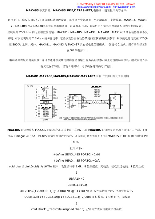
max3485中文资料
max485接口芯片是Maxim公司的一种RS-485芯片。
简介:MAX485、MAX487-MAX491以及MAX1487是用于RS-485与RS-422通信的低功耗收发器,每个器件中都具有一个驱动器和一个接收器。
MAX483、MAX487、MAX488以及MAX489具有限摆率驱动器,可以减小EMI,并降低由不恰当的终端匹配电缆引起的反射,实现最高250kbps的无差错数据传输。
MAX481、MAX485、MAX490、MAX491、MAX1487的驱动器摆率不受限制,可以实现最高2.5Mbps的传输速率。
这些收发器在驱动器禁用的空载或满载状态下,吸取的电源电流在120µA至500µA之间。
另外,MAX481、MAX483与MAX487具有低电流关断模式,仅消耗0.1µA。
所有器件都工作在5V单电源下。
采用单一电源+5 V工作,额定电流为300 μA,采用半双工通讯方式。
它完成将TTL电平转换为RS-485电平的功能。
MAX485芯片的结构和引脚都非常简单,内部含有一个驱动器和接收器。
RO和DI 端分别为接收器的输出和驱动器的输入端,与单片机连接时只需分别与单片机的RXD和TXD相连即可;/RE和DE端分别为接收和发送的使能端,当/RE为逻辑0时,器件处于接收状态;当DE为逻辑1时,器件处于发送状态,因为MAX485工作在半双工状态,所以只需用单片机的一个管脚控制这两个引脚即可;A端和B端分别为接收和发送的差分信号端,当A引脚的电平高于B时,代表发送的数据为1;当A的电平低于B端时,代表发送的数据为0。
在与单片机连接时接线非常简单。
只需要一个信号控制MAX485的接收和发送即可。
同时将A和B端之间加匹配电阻,一般可选100Ω的电阻。
基本参数:半双工;限摆率:NO;低电流关断模式:NO;接收允许控制:YES;静态电流300uA;引脚数:8。
Max485使用说明
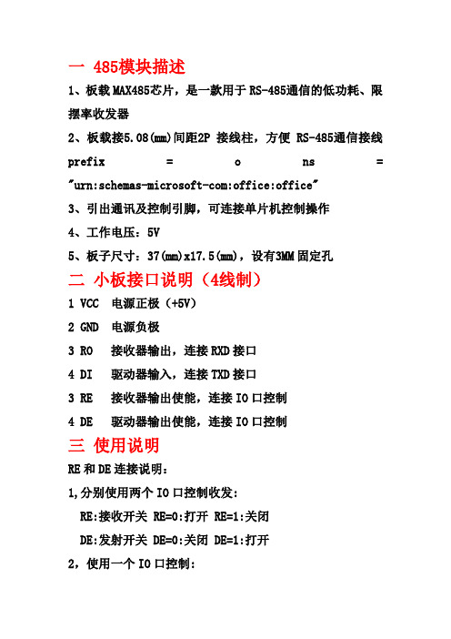
一 485模块描述
1、板载MAX485芯片,是一款用于RS-485通信的低功耗、限摆率收发器
2、板载接5.08(mm)间距2P接线柱,方便RS-485通信接线prefix = o ns = "urn:schemas-microsoft-com:office:office"
3、引出通讯及控制引脚,可连接单片机控制操作
4、工作电压:5V
5、板子尺寸:37(mm)x17.5(mm),设有3MM固定孔
二小板接口说明(4线制)
1 VCC 电源正极(+5V)
2 GND 电源负极
3 RO 接收器输出,连接RXD接口
4 DI 驱动器输入,连接TXD接口
3 RE 接收器输出使能,连接IO口控制
4 DE 驱动器输出使能,连接IO口控制
三使用说明
RE和DE连接说明:
1,分别使用两个IO口控制收发:
RE:接收开关 RE=0:打开 RE=1:关闭
DE:发射开关 DE=0:关闭 DE=1:打开
2,使用一个IO口控制:
RE和DE相连接至一个IO口,IO=0:只接收,IO=1:只发射参考图如下:
两种控制方式取决于系统的设计
3,如果你的系统只有RXD和TXD信号而无控制IO口,则可以由外部直接打开使能,但注意,只能做发射器或接收器。
因板带上拉电阻,RE和DE不连接时(悬空)为高电平,即只做发射器,如需改为接收器使用,则将RE和DE接低电平(接GND端)。
MAX485CSA+中文资料

For pricing, delivery, and ordering information,please contact Maxim/Dallas Direct!at 1-888-629-4642, or visit Maxim’s website at .General DescriptionThe MAX481, MAX483, MAX485, MAX487–MAX491, and MAX1487 are low-power transceivers for RS-485 and RS-422 communication. Each part contains one driver and one receiver. The MAX483, MAX487, MAX488, and MAX489feature reduced slew-rate drivers that minimize EMI and reduce reflections caused by improperly terminated cables,thus allowing error-free data transmission up to 250kbps.The driver slew rates of the MAX481, MAX485, MAX490,MAX491, and MAX1487 are not limited, allowing them to transmit up to 2.5Mbps.These transceivers draw between 120µA and 500µA of supply current when unloaded or fully loaded with disabled drivers. Additionally, the MAX481, MAX483, and MAX487have a low-current shutdown mode in which they consume only 0.1µA. All parts operate from a single 5V supply.Drivers are short-circuit current limited and are protected against excessive power dissipation by thermal shutdown circuitry that places the driver outputs into a high-imped-ance state. The receiver input has a fail-safe feature that guarantees a logic-high output if the input is open circuit.The MAX487 and MAX1487 feature quarter-unit-load receiver input impedance, allowing up to 128 MAX487/MAX1487 transceivers on the bus. Full-duplex communi-cations are obtained using the MAX488–MAX491, while the MAX481, MAX483, MAX485, MAX487, and MAX1487are designed for half-duplex applications.________________________ApplicationsLow-Power RS-485 Transceivers Low-Power RS-422 Transceivers Level TranslatorsTransceivers for EMI-Sensitive Applications Industrial-Control Local Area Networks__Next Generation Device Features♦For Fault-Tolerant ApplicationsMAX3430: ±80V Fault-Protected, Fail-Safe, 1/4Unit Load, +3.3V, RS-485 TransceiverMAX3440E–MAX3444E: ±15kV ESD-Protected,±60V Fault-Protected, 10Mbps, Fail-Safe, RS-485/J1708 Transceivers♦For Space-Constrained ApplicationsMAX3460–MAX3464: +5V, Fail-Safe, 20Mbps,Profibus RS-485/RS-422 TransceiversMAX3362: +3.3V, High-Speed, RS-485/RS-422Transceiver in a SOT23 PackageMAX3280E–MAX3284E: ±15kV ESD-Protected,52Mbps, +3V to +5.5V, SOT23, RS-485/RS-422,True Fail-Safe ReceiversMAX3293/MAX3294/MAX3295: 20Mbps, +3.3V,SOT23, RS-855/RS-422 Transmitters ♦For Multiple Transceiver ApplicationsMAX3030E–MAX3033E: ±15kV ESD-Protected,+3.3V, Quad RS-422 Transmitters ♦For Fail-Safe ApplicationsMAX3080–MAX3089: Fail-Safe, High-Speed (10Mbps), Slew-Rate-Limited RS-485/RS-422Transceivers♦For Low-Voltage ApplicationsMAX3483E/MAX3485E/MAX3486E/MAX3488E/MAX3490E/MAX3491E: +3.3V Powered, ±15kV ESD-Protected, 12Mbps, Slew-Rate-Limited,True RS-485/RS-422 TransceiversMAX481/MAX483/MAX485/MAX487–MAX491/MAX1487Low-Power, Slew-Rate-Limited RS-485/RS-422 Transceivers______________________________________________________________Selection Table19-0122; Rev 8; 10/03Ordering Information appears at end of data sheet.M A X 481/M A X 483/M A X 485/M A X 487–M A X 491/M A X 1487Low-Power, Slew-Rate-Limited RS-485/RS-422 Transceivers 2_______________________________________________________________________________________ABSOLUTE MAXIMUM RATINGSSupply Voltage (V CC ).............................................................12V Control Input Voltage (RE , DE)...................-0.5V to (V CC + 0.5V)Driver Input Voltage (DI).............................-0.5V to (V CC + 0.5V)Driver Output Voltage (A, B)...................................-8V to +12.5V Receiver Input Voltage (A, B).................................-8V to +12.5V Receiver Output Voltage (RO).....................-0.5V to (V CC +0.5V)Continuous Power Dissipation (T A = +70°C)8-Pin Plastic DIP (derate 9.09mW/°C above +70°C)....727mW 14-Pin Plastic DIP (derate 10.00mW/°C above +70°C)..800mW 8-Pin SO (derate 5.88mW/°C above +70°C).................471mW14-Pin SO (derate 8.33mW/°C above +70°C)...............667mW 8-Pin µMAX (derate 4.1mW/°C above +70°C)..............830mW 8-Pin CERDIP (derate 8.00mW/°C above +70°C).........640mW 14-Pin CERDIP (derate 9.09mW/°C above +70°C).......727mW Operating Temperature RangesMAX4_ _C_ _/MAX1487C_ A...............................0°C to +70°C MAX4__E_ _/MAX1487E_ A.............................-40°C to +85°C MAX4__MJ_/MAX1487MJA...........................-55°C to +125°C Storage Temperature Range.............................-65°C to +160°C Lead Temperature (soldering, 10sec).............................+300°CDC ELECTRICAL CHARACTERISTICS(V CC = 5V ±5%, T A = T MIN to T MAX , unless otherwise noted.) (Notes 1, 2)Stresses beyond those listed under “Absolute Maximum Ratings” may cause permanent damage to the device. These are stress ratings only, and functional operation of the device at these or any other conditions beyond those indicated in the operational sections of the specifications is not implied. Exposure to absolute maximum rating conditions for extended periods may affect device reliability.VV IN = -7VV IN = 12V V IN = -7V V IN = 12V Input Current (A, B)I IN2V TH k Ω48-7V ≤V CM ≤12V, MAX487/MAX1487R INReceiver Input Resistance -7V ≤V CM ≤12V, all devices except MAX487/MAX1487R = 27Ω(RS-485), Figure 40.4V ≤V O ≤2.4VR = 50Ω(RS-422)I O = 4mA, V ID = -200mV I O = -4mA, V ID = 200mV V CM = 0V-7V ≤V CM ≤12V DE, DI, RE DE, DI, RE MAX487/MAX1487,DE = 0V, V CC = 0V or 5.25VDE, DI, RE R = 27Ωor 50Ω, Figure 4R = 27Ωor 50Ω, Figure 4R = 27Ωor 50Ω, Figure 4DE = 0V;V CC = 0V or 5.25V,all devices except MAX487/MAX1487CONDITIONSk Ω12µA ±1I OZRThree-State (high impedance)Output Current at ReceiverV 0.4V OL Receiver Output Low Voltage 3.5V OH Receiver Output High Voltage mV 70∆V TH Receiver Input Hysteresis V -0.20.2Receiver Differential Threshold Voltage-0.2mA 0.25mA-0.81.01.55V OD2Differential Driver Output (with load)V 2V 5V OD1Differential Driver Output (no load)µA±2I IN1Input CurrentV 0.8V IL Input Low Voltage V 2.0V IH Input High Voltage V 0.2∆V OD Change in Magnitude of Driver Common-Mode Output Voltage for Complementary Output States V 0.2∆V OD Change in Magnitude of Driver Differential Output Voltage for Complementary Output States V 3V OC Driver Common-Mode Output VoltageUNITS MINTYPMAX SYMBOL PARAMETERMAX481/MAX483/MAX485/MAX487–MAX491/MAX1487Low-Power, Slew-Rate-Limited RS-485/RS-422 Transceivers_______________________________________________________________________________________3SWITCHING CHARACTERISTICS—MAX481/MAX485, MAX490/MAX491, MAX1487(V CC = 5V ±5%, T A = T MIN to T MAX , unless otherwise noted.) (Notes 1, 2)DC ELECTRICAL CHARACTERISTICS (continued)(V CC = 5V ±5%, T A = T MIN to T MAX , unless otherwise noted.) (Notes 1, 2)ns 103060t PHLDriver Rise or Fall Time Figures 6 and 8, R DIFF = 54Ω, C L1= C L2= 100pF ns MAX490M, MAX491M MAX490C/E, MAX491C/E2090150MAX481, MAX485, MAX1487MAX490M, MAX491MMAX490C/E, MAX491C/E MAX481, MAX485, MAX1487Figures 6 and 8, R DIFF = 54Ω,C L1= C L2= 100pF MAX481 (Note 5)Figures 5 and 11, C RL = 15pF, S2 closedFigures 5 and 11, C RL = 15pF, S1 closed Figures 5 and 11, C RL = 15pF, S2 closed Figures 5 and 11, C RL = 15pF, S1 closed Figures 6 and 10, R DIFF = 54Ω,C L1= C L2= 100pFFigures 6 and 8,R DIFF = 54Ω,C L1= C L2= 100pF Figures 6 and 10,R DIFF = 54Ω,C L1= C L2= 100pF CONDITIONS ns 510t SKEW ns50200600t SHDNTime to ShutdownMbps 2.5f MAX Maximum Data Rate ns 2050t HZ Receiver Disable Time from High ns 103060t PLH 2050t LZ Receiver Disable Time from Low ns 2050t ZH Driver Input to Output Receiver Enable to Output High ns 2050t ZL Receiver Enable to Output Low 2090200ns ns 134070t HZ t SKD Driver Disable Time from High |t PLH - t PHL |DifferentialReceiver Skewns 4070t LZ Driver Disable Time from Low ns 4070t ZL Driver Enable to Output Low 31540ns51525ns 31540t R , t F 2090200Driver Output Skew to Output t PLH , t PHL Receiver Input to Output4070t ZH Driver Enable to Output High UNITS MIN TYP MAX SYMBOL PARAMETERFigures 7 and 9, C L = 100pF, S2 closed Figures 7 and 9, C L = 100pF, S1 closed Figures 7 and 9, C L = 15pF, S1 closed Figures 7 and 9, C L = 15pF, S2 closedM A X 481/M A X 483/M A X 485/M A X 487–M A X 491/M A X 1487Low-Power, Slew-Rate-Limited RS-485/RS-422 Transceivers 4_______________________________________________________________________________________SWITCHING CHARACTERISTICS—MAX483, MAX487/MAX488/MAX489(V CC = 5V ±5%, T A = T MIN to T MAX , unless otherwise noted.) (Notes 1, 2)SWITCHING CHARACTERISTICS—MAX481/MAX485, MAX490/MAX491, MAX1487 (continued)(V CC = 5V ±5%, T A = T MIN to T MAX , unless otherwise noted.) (Notes 1, 2)3001000Figures 7 and 9, C L = 100pF, S2 closed Figures 7 and 9, C L = 100pF, S1 closed Figures 5 and 11, C L = 15pF, S2 closed,A - B = 2VCONDITIONSns 40100t ZH(SHDN)Driver Enable from Shutdown toOutput High (MAX481)nsFigures 5 and 11, C L = 15pF, S1 closed,B - A = 2Vt ZL(SHDN)Receiver Enable from Shutdownto Output Low (MAX481)ns 40100t ZL(SHDN)Driver Enable from Shutdown toOutput Low (MAX481)ns 3001000t ZH(SHDN)Receiver Enable from Shutdownto Output High (MAX481)UNITS MINTYP MAX SYMBOLPARAMETERtPLH t SKEW Figures 6 and 8, R DIFF = 54Ω,C L1= C L2= 100pFt PHL Figures 6 and 8, R DIFF = 54Ω,C L1= C L2= 100pFDriver Input to Output Driver Output Skew to Output ns 100800ns ns 2000MAX483/MAX487, Figures 7 and 9,C L = 100pF, S2 closedt ZH(SHDN)Driver Enable from Shutdown to Output High2502000ns2500MAX483/MAX487, Figures 5 and 11,C L = 15pF, S1 closedt ZL(SHDN)Receiver Enable from Shutdown to Output Lowns 2500MAX483/MAX487, Figures 5 and 11,C L = 15pF, S2 closedt ZH(SHDN)Receiver Enable from Shutdown to Output Highns 2000MAX483/MAX487, Figures 7 and 9,C L = 100pF, S1 closedt ZL(SHDN)Driver Enable from Shutdown to Output Lowns 50200600MAX483/MAX487 (Note 5) t SHDN Time to Shutdownt PHL t PLH , t PHL < 50% of data period Figures 5 and 11, C RL = 15pF, S2 closed Figures 5 and 11, C RL = 15pF, S1 closed Figures 5 and 11, C RL = 15pF, S2 closed Figures 5 and 11, C RL = 15pF, S1 closed Figures 7 and 9, C L = 15pF, S2 closed Figures 6 and 10, R DIFF = 54Ω,C L1= C L2= 100pFFigures 7 and 9, C L = 15pF, S1 closed Figures 7 and 9, C L = 100pF, S1 closed Figures 7 and 9, C L = 100pF, S2 closed CONDITIONSkbps 250f MAX 2508002000Maximum Data Rate ns 2050t HZ Receiver Disable Time from High ns 25080020002050t LZ Receiver Disable Time from Low ns 2050t ZH Receiver Enable to Output High ns 2050t ZL Receiver Enable to Output Low ns ns 1003003000t HZ t SKD Driver Disable Time from High I t PLH - t PHL I DifferentialReceiver SkewFigures 6 and 10, R DIFF = 54Ω,C L1= C L2= 100pFns 3003000t LZ Driver Disable Time from Low ns 2502000t ZL Driver Enable to Output Low ns Figures 6 and 8, R DIFF = 54Ω,C L1= C L2= 100pFns 2502000t R , t F 2502000Driver Rise or Fall Time ns t PLH Receiver Input to Output2502000t ZH Driver Enable to Output High UNITS MIN TYP MAX SYMBOL PARAMETERMAX481/MAX483/MAX485/MAX487–MAX491/MAX1487Low-Power, Slew-Rate-Limited RS-485/RS-422 Transceivers_______________________________________________________________________________________530002.5OUTPUT CURRENT vs.RECEIVER OUTPUT LOW VOLTAGE525M A X 481-01OUTPUT LOW VOLTAGE (V)O U T P U T C U R R E N T (m A )1.515100.51.02.0203540450.90.1-50-252575RECEIVER OUTPUT LOW VOLTAGE vs.TEMPERATURE0.30.7TEMPERATURE (°C)O U T P U TL O W V O L T A G E (V )500.50.80.20.60.40100125-20-41.5 2.0 3.0 5.0OUTPUT CURRENT vs.RECEIVER OUTPUT HIGH VOLTAGE-8-16M A X 481-02OUTPUT HIGH VOLTAGE (V)O U T P U T C U R R E N T (m A )2.5 4.0-12-18-6-14-10-203.54.5 4.83.2-50-252575RECEIVER OUTPUT HIGH VOLTAGE vs.TEMPERATURE3.64.4TEMPERATURE (°C)O U T P UT H I G H V O L T A G E (V )0504.04.63.44.23.83.01001259000 1.0 3.0 4.5DRIVER OUTPUT CURRENT vs.DIFFERENTIAL OUTPUT VOLTAGE1070M A X 481-05DIFFERENTIAL OUTPUT VOLTAGE (V)O U T P U T C U R R E N T (m A )2.0 4.05030806040200.5 1.5 2.53.5 2.31.5-50-2525125DRIVER DIFFERENTIAL OUTPUT VOLTAGEvs. TEMPERATURE1.72.1TEMPERATURE (°C)D I F FE R E N T I A L O U T P U TV O L T A G E (V )751.92.21.62.01.8100502.4__________________________________________Typical Operating Characteristics(V CC = 5V, T A = +25°C, unless otherwise noted.)NOTES FOR ELECTRICAL/SWITCHING CHARACTERISTICSNote 1:All currents into device pins are positive; all currents out of device pins are negative. All voltages are referenced to deviceground unless otherwise specified.Note 2:All typical specifications are given for V CC = 5V and T A = +25°C.Note 3:Supply current specification is valid for loaded transmitters when DE = 0V.Note 4:Applies to peak current. See Typical Operating Characteristics.Note 5:The MAX481/MAX483/MAX487 are put into shutdown by bringing RE high and DE low. If the inputs are in this state for lessthan 50ns, the parts are guaranteed not to enter shutdown. If the inputs are in this state for at least 600ns, the parts are guaranteed to have entered shutdown. See Low-Power Shutdown Mode section.M A X 481/M A X 483/M A X 485/M A X 487–M A X 491/M A X 1487Low-Power, Slew-Rate-Limited RS-485/RS-422 Transceivers 6___________________________________________________________________________________________________________________Typical Operating Characteristics (continued)(V CC = 5V, T A = +25°C, unless otherwise noted.)120008OUTPUT CURRENT vs.DRIVER OUTPUT LOW VOLTAGE20100M A X 481-07OUTPUT LOW VOLTAGE (V)O U T P U T C U R R E N T (m A )6604024801012140-1200-7-5-15OUTPUT CURRENT vs.DRIVER OUTPUT HIGH VOLTAGE-20-80M A X 481-08OUTPUT HIGH VOLTAGE (V)O U T P U T C U R R E N T (m A )-31-603-6-4-2024-100-40100-40-60-2040100120MAX1487SUPPLY CURRENT vs. TEMPERATURE300TEMPERATURE (°C)S U P P L Y C U R R E N T (µA )20608050020060040000140100-50-2550100MAX481/MAX485/MAX490/MAX491SUPPLY CURRENT vs. TEMPERATURE300TEMPERATURE (°C)S U P P L Y C U R R E N T (µA )257550020060040000125100-50-2550100MAX483/MAX487–MAX489SUPPLY CURRENT vs. TEMPERATURE300TEMPERATURE (°C)S U P P L Y C U R R E N T (µA )257550020060040000125MAX481/MAX483/MAX485/MAX487–MAX491/MAX1487Low-Power, Slew-Rate-Limited RS-485/RS-422 Transceivers_______________________________________________________________________________________7______________________________________________________________Pin DescriptionFigure 1. MAX481/MAX483/MAX485/MAX487/MAX1487 Pin Configuration and Typical Operating CircuitM A X 481/M A X 483/M A X 485/M A X 487–M A X 491/M A X 1487__________Applications InformationThe MAX481/MAX483/MAX485/MAX487–MAX491 and MAX1487 are low-power transceivers for RS-485 and RS-422 communications. The MAX481, MAX485, MAX490,MAX491, and MAX1487 can transmit and receive at data rates up to 2.5Mbps, while the MAX483, MAX487,MAX488, and MAX489 are specified for data rates up to 250kbps. The MAX488–MAX491 are full-duplex trans-ceivers while the MAX481, MAX483, MAX485, MAX487,and MAX1487 are half-duplex. In addition, Driver Enable (DE) and Receiver Enable (RE) pins are included on the MAX481, MAX483, MAX485, MAX487, MAX489,MAX491, and MAX1487. When disabled, the driver and receiver outputs are high impedance.MAX487/MAX1487:128 Transceivers on the BusThe 48k Ω, 1/4-unit-load receiver input impedance of the MAX487 and MAX1487 allows up to 128 transceivers on a bus, compared to the 1-unit load (12k Ωinput impedance) of standard RS-485 drivers (32 trans-ceivers maximum). Any combination of MAX487/MAX1487 and other RS-485 transceivers with a total of 32 unit loads or less can be put on the bus. The MAX481/MAX483/MAX485 and MAX488–MAX491 have standard 12k ΩReceiver Input impedance.Low-Power, Slew-Rate-Limited RS-485/RS-422 Transceivers 8_______________________________________________________________________________________Figure 2. MAX488/MAX490 Pin Configuration and Typical Operating CircuitFigure 3. MAX489/MAX491 Pin Configuration and Typical Operating CircuitMAX483/MAX487/MAX488/MAX489:Reduced EMI and ReflectionsThe MAX483 and MAX487–MAX489 are slew-rate limit-ed, minimizing EMI and reducing reflections caused by improperly terminated cables. Figure 12 shows the dri-ver output waveform and its Fourier analysis of a 150kHz signal transmitted by a MAX481, MAX485,MAX490, MAX491, or MAX1487. High-frequency har-monics with large amplitudes are evident. Figure 13shows the same information displayed for a MAX483,MAX487, MAX488, or MAX489 transmitting under the same conditions. Figure 13’s high-frequency harmonics have much lower amplitudes, and the potential for EMI is significantly reduced.MAX481/MAX483/MAX485/MAX487–MAX491/MAX1487Low-Power, Slew-Rate-Limited RS-485/RS-422 Transceivers_______________________________________________________________________________________9_________________________________________________________________Test CircuitsFigure 4. Driver DC Test Load Figure 5. Receiver Timing Test LoadFigure 6. Driver/Receiver Timing Test Circuit Figure 7. Driver Timing Test LoadM A X 481/M A X 483/M A X 485/M A X 487–M A X 491/M A X 1487Low-Power, Slew-Rate-Limited RS-485/RS-422 Transceivers 10_______________________________________________________Switching Waveforms_________________Function Tables (MAX481/MAX483/MAX485/MAX487/MAX1487)Figure 8. Driver Propagation DelaysFigure 9. Driver Enable and Disable Times (except MAX488 and MAX490)Figure 10. Receiver Propagation DelaysFigure 11. Receiver Enable and Disable Times (except MAX488and MAX490)Table 1. TransmittingTable 2. ReceivingLow-Power Shutdown Mode (MAX481/MAX483/MAX487)A low-power shutdown mode is initiated by bringing both RE high and DE low. The devices will not shut down unless both the driver and receiver are disabled.In shutdown, the devices typically draw only 0.1µA of supply current.RE and DE may be driven simultaneously; the parts are guaranteed not to enter shutdown if RE is high and DE is low for less than 50ns. If the inputs are in this state for at least 600ns, the parts are guaranteed to entershutdown.For the MAX481, MAX483, and MAX487, the t ZH and t ZL enable times assume the part was not in the low-power shutdown state (the MAX485/MAX488–MAX491and MAX1487 can not be shut down). The tZH(SHDN)and t ZL(SHDN)enable times assume the parts were shut down (see Electrical Characteristics ).It takes the drivers and receivers longer to become enabled from the low-power shutdown state(t ZH(SHDN ), t ZL(SHDN)) than from the operating mode(t ZH , t ZL ). (The parts are in operating mode if the –R —E –,DE inputs equal a logical 0,1 or 1,1 or 0, 0.)Driver Output Protection Excessive output current and power dissipation causedby faults or by bus contention are prevented by two mechanisms. A foldback current limit on the output stage provides immediate protection against short cir-cuits over the whole common-mode voltage range (see Typical Operating Characteristics ). In addition, a ther-mal shutdown circuit forces the driver outputs into a high-impedance state if the die temperature rises excessively.Propagation DelayMany digital encoding schemes depend on the differ-ence between the driver and receiver propagation delay times. Typical propagation delays are shown in Figures 15–18 using Figure 14’s test circuit.The difference in receiver delay times, | t PLH - t PHL |, istypically under 13ns for the MAX481, MAX485,MAX490, MAX491, and MAX1487 and is typically lessthan 100ns for the MAX483 and MAX487–MAX489.The driver skew times are typically 5ns (10ns max) for the MAX481, MAX485, MAX490, MAX491, and MAX1487, and are typically 100ns (800ns max) for theMAX483 and MAX487–MAX489.MAX481/MAX483/MAX485/MAX487–MAX491/MAX1487Low-Power, Slew-Rate-Limited RS-485/RS-422 Transceivers______________________________________________________________________________________1110dB/div0Hz 5MHz 500kHz/div 10dB/div0Hz 5MHz500kHz/divFigure 12. Driver Output Waveform and FFT Plot of MAX481/MAX485/MAX490/MAX491/MAX1487 Transmitting a 150kHzSignalFigure 13. Driver Output Waveform and FFT Plot of MAX483/MAX487–MAX489 Transmitting a 150kHz SignalM A X 481/M A X 483/M A X 485/M A X 487–M A X 491/M A X 1487Low-Power, Slew-Rate-Limited RS-485/RS-422 Transceivers12______________________________________________________________________________________V CC = 5V T A = +25°C V CC = 5V T A = +25°C V CC = 5V T A = +25°CV CC = 5V T A = +25°C Figure 14. Receiver Propagation Delay Test Circuit Figure 15. MAX481/MAX485/MAX490/MAX491/MAX1487Receiver t PHL Figure 16. MAX481/MAX485/MAX490/MAX491/MAX1487Receiver t PLH PHL Figure 18. MAX483, MAX487–MAX489 Receiver t PLHLine Length vs. Data Rate The RS-485/RS-422 standard covers line lengths up to 4000 feet. For line lengths greater than 4000 feet, see Figure 23.Figures 19 and 20 show the system differential voltage for the parts driving 4000 feet of 26AWG twisted-pair wire at 110kHz into 120Ωloads.Typical Applications The MAX481, MAX483, MAX485, MAX487–MAX491, and MAX1487 transceivers are designed for bidirectional datacommunications on multipoint bus transmission lines.Figures 21 and 22 show typical network applications circuits. These parts can also be used as line repeaters, with cable lengths longer than 4000 feet, as shown in Figure 23.To minimize reflections, the line should be terminated at both ends in its characteristic impedance, and stub lengths off the main line should be kept as short as possi-ble. The slew-rate-limited MAX483 and MAX487–MAX489are more tolerant of imperfect termination.MAX481/MAX483/MAX485/MAX487–MAX491/MAX1487Low-Power, Slew-Rate-Limited RS-485/RS-422 Transceivers______________________________________________________________________________________13DI V Y -V Z RO 5V 0V 1V 0V -1V 5V 0V 2µs/divFigure 19. MAX481/MAX485/MAX490/MAX491/MAX1487 System Differential Voltage at 110kHz Driving 4000ft of Cable Figure 20. MAX483, MAX487–MAX489 System Differential Voltage at 110kHz Driving 4000ft of CableFigure 21. MAX481/MAX483/MAX485/MAX487/MAX1487 Typical Half-Duplex RS-485 NetworkM A X 481/M A X 483/M A X 485/M A X 487–M A X 491/M A X 1487Low-Power, Slew-Rate-Limited RS-485/RS-422 Transceivers14______________________________________________________________________________________Figure 22. MAX488–MAX491 Full-Duplex RS-485 NetworkFigure 23. Line Repeater for MAX488–MAX491Isolated RS-485For isolated RS-485 applications, see the MAX253 and MAX1480 data sheets.MAX481/MAX483/MAX485/MAX487–MAX491/MAX1487Low-Power, Slew-Rate-Limited RS-485/RS-422 Transceivers______________________________________________________________________________________15_______________Ordering Information _________________Chip Topographies MAX481/MAX483/MAX485/MAX487/MAX1487N.C. RO 0.054"(1.372mm)0.080"(2.032mm)DE DI GNDB N.C.VCCA RE * Contact factory for dice specifications.__Ordering Information (continued)M A X 481/M A X 483/M A X 485/M A X 487–M A X 491/M A X 1487Low-Power, Slew-Rate-Limited RS-485/RS-422 Transceivers16______________________________________________________________________________________TRANSISTOR COUNT: 248SUBSTRATE CONNECTED TO GNDMAX488/MAX490B RO 0.054"(1.372mm)0.080"(2.032mm) N.C. DI GND Z A V CC Y N.C._____________________________________________Chip Topographies (continued)MAX489/MAX491B RO 0.054"(1.372mm)0.080"(2.032mm) DE DI GND Z A V CC Y REMAX481/MAX483/MAX485/MAX487–MAX491/MAX1487Low-Power, Slew-Rate-Limited RS-485/RS-422 Transceivers______________________________________________________________________________________17Package Information(The package drawing(s) in this data sheet may not reflect the most current specifications. For the latest package outline information go to /packages .)SO IC N.E PSM A X 481/M A X 483/M A X 485/M A X 487–M A X 491/M A X 1487Low-Power, Slew-Rate-Limited RS-485/RS-422 Transceivers18______________________________________________________________________________________Package Information (continued)(The package drawing(s) in this data sheet may not reflect the most current specifications. For the latest package outline information go to /packages .)MAX481/MAX483/MAX485/MAX487–MAX491Low-Power, Slew-Rate-Limited RS-485/RS-422 TransceiversMaxim cannot assume responsibility for use of any circuitry other than circuitry entirely embodied in a Maxim product. No circuit patent licenses areimplied. Maxim reserves the right to change the circuitry and specifications without notice at any time.Maxim Integrated Products, 120 San Gabriel Drive, Sunnyvale, CA 94086 408-737-7600 ____________________19©2003 Maxim Integrated Products Printed USAis a registered trademark of Maxim Integrated Products.M A X 481/M A X 483/M A X 485/M A X 487–M A X 491/M A X 1487PD I P N.E PS Package Information (continued)(The package drawing(s) in this data sheet may not reflect the most current specifications. For the latest package outline information go to /packages.)。
max485esa中文资料
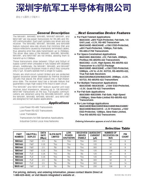
General DescriptionThe MAX481, MAX483, MAX485, MAX487–MAX491, andMAX1487 are low-power transceivers for RS-485 and RS-422 communication. Each part contains one driver and onereceiver. The MAX483, MAX487, MAX488, and MAX489feature reduced slew-rate drivers that minimize E MI andreduce reflections caused by improperly terminated cables,thus allowing error-free data transmission up to 250kbps.The driver slew rates of the MAX481, MAX485, MAX490,MAX491, and MAX1487 are not limited, allowing them totransmit up to 2.5Mbps.These transceivers draw between 120µA and 500µA ofsupply current when unloaded or fully loaded with disableddrivers. Additionally, the MAX481, MAX483, and MAX487have a low-current shutdown mode in which they consumeonly 0.1µA. All parts operate from a single 5V supply.Drivers are short-circuit current limited and are protectedagainst excessive power dissipation by thermal shutdowncircuitry that places the driver outputs into a high-imped-ance state. The receiver input has a fail-safe feature thatguarantees a logic-high output if the input is open circuit.The MAX487 and MAX1487 feature quarter-unit-loadreceiver input impedance, allowing up to 128 MAX487/MAX1487 transceivers on the bus. Full-duplex communi-cations are obtained using the MAX488–MAX491, whilethe MAX481, MAX483, MAX485, MAX487, and MAX1487are designed for half-duplex applications.________________________Applications Low-Power RS-485 Transceivers Low-Power RS-422 Transceivers Level Translators Transceivers for EMI-Sensitive Applications Industrial-Control Local Area Networks__Next Generation Device Features o For Fault-Tolerant Applications MAX3430: ±80V Fault-Protected, Fail-Safe, 1/4Unit Load, +3.3V, RS-485 Transceiver MAX3440E–MAX3444E: ±15kV ESD-Protected,±60V Fault-Protected, 10Mbps, Fail-Safe, RS-485/J1708 Transceivers o For Space-Constrained Applications MAX3460–MAX3464: +5V, Fail-Safe, 20Mbps,Profibus RS-485/RS-422 Transceivers MAX3362: +3.3V, High-Speed, RS-485/RS-422Transceiver in a SOT23 Package MAX3280E–MAX3284E: ±15kV ESD-Protected,52Mbps, +3V to +5.5V, SOT23, RS-485/RS-422,True Fail-Safe Receivers MAX3293/MAX3294/MAX3295: 20Mbps, +3.3V,SOT23, RS-485/RS-422 Transmitters o For Multiple Transceiver Applications MAX3030E–MAX3033E: ±15kV ESD-Protected,+3.3V, Quad RS-422 Transmitters o For Fail-Safe Applications MAX3080–MAX3089: Fail-Safe, High-Speed (10Mbps), Slew-Rate-Limited RS-485/RS-422Transceiverso For Low-Voltage ApplicationsMAX3483E/MAX3485E/MAX3486E/MAX3488E/MAX3490E/MAX3491E: +3.3V Powered, ±15kVESD-Protected, 12Mbps, Slew-Rate-Limited,True RS-485/RS-422 Transceivers For pricing, delivery, and ordering information, please contact Maxim Direct at1-888-629-4642, or visit Maxim Integrated’s website at .______________________________________________________________Selection Table19-0122; Rev 10; 9/14PARTNUMBERHALF/FULL DUPLEX DATA RATE (Mbps) SLEW-RATE LIMITED LOW-POWER SHUTDOWN RECEIVER/DRIVER ENABLE QUIESCENT CURRENT (μA) NUMBER OF RECEIVERS ON BUS PIN COUNT MAX481Half 2.5No Yes Yes 300328MAX483Half 0.25Yes Yes Yes 120328MAX485Half 2.5No No Yes 300328MAX487Half 0.25Yes Yes Yes 1201288MAX488Full 0.25Yes No No 120328MAX489Full 0.25Yes No Yes 1203214MAX490Full 2.5No No No 300328MAX491Full 2.5No No Yes 3003214MAX1487 Half 2.5No No Yes 2301288Ordering Information appears at end of data sheet.找电子元器件上宇航军工MAX481/MAX483/MAX485/MAX487–MAX491/MAX1487Low-Power, Slew-Rate-LimitedRS-485/RS-422 TransceiversPackage Information For the latest package outline information and land patterns, go to . Note that a “+”, “#”, or “-”in the package code indicates RoHS status only. Package drawings may show a different suffix character, but the drawing pertains to the package regardless of RoHS status.16Low-Power, Slew-Rate-Limited RS-485/RS-422 TransceiversMAX481/MAX483/MAX485/MAX487–MAX491/MAX1487Maxim Integrated cannot assume responsibility for use of any circuitry other than circuitry entirely embodied in a Maxim Integrated product. No circuit patent licenses are implied. Maxim Integrated reserves the right to change the circuitry and specifications without notice at any time. The parametric values (min and max limits) shown in the Electrical Characteristics table are guaranteed. Other parametric values quoted in this data sheet are provided for guidance.Maxim Integrated 160 Rio Robles, San Jose, CA 95134 USA 1-408-601-100017©2014 Maxim Integrated Products, Inc.Maxim Integrated and the Maxim Integrated logo are trademarks of Maxim Integrated Products, Inc.。
- 1、下载文档前请自行甄别文档内容的完整性,平台不提供额外的编辑、内容补充、找答案等附加服务。
- 2、"仅部分预览"的文档,不可在线预览部分如存在完整性等问题,可反馈申请退款(可完整预览的文档不适用该条件!)。
- 3、如文档侵犯您的权益,请联系客服反馈,我们会尽快为您处理(人工客服工作时间:9:00-18:30)。
```````````````````````````````````গၤNBY24596F0NBY24597Fဵ,6W࢟ĂۍၷĂᎌ±26lW!FTEۣઐࡼST.596၃खLj۞ጙവདࣅਜ਼ጙവ၃ăᑚೝୈ۞౪ပۣઐ࢟വLjᏴ၃ၒྜྷఎവവࡼ༽ౚሆཀྵۣၒ߲൝࢟ຳăྙਫਂᏴ࣡ᔐሣࡼჅᎌख႙ۻண)ᔜ*Lj၃ၒ߲൝࢟ຳăNBY24596F0NBY24597FᎌེރڰถLjభጲሿ߹ེ࢟ރྜྷဟᔐሣࡼ৺ᑇၾܤቧăNBY24596FᎌሢڼൈདࣅLjถ৫ଢ଼ࢅFNJਜ਼ݙࡩࡼ࢟಄࣡ჅࡼनLjဣሚࡉ611lcqtࡼᇄᇙ൩ၫࠅၒăNBY24597Fདࣅᎌ࣪ڼൈଝጲሢᒜLjᏤࡉ27NcqtࡼࠅၒႥൈăNBY24596F0NBY24597Fࡼ၃ၒྜྷᔜఝᆐ205ᆡঌᏲLjᏤࣶࡉ239ৈ၃खਂᏴᔐሣLjೝୈ᎖ۍၷᄰቧăჅᎌདࣅၒ߲ᄋ±26lWཽᄏෝါFTEۣઐăNBY24596F0NBY24597Fݧ9୭TPஂဏహମࡼ9୭μEGOॖᓤLjᔫ᎖.51°Dᒗ,96°D౫ᐱᆨࣞपᆍă```````````````````````````````````።࢟ܭጓ఼ᒜጓ࢟૦དࣅᔈࣅIWBDᇹᄻ```````````````````````````````````ᄂቶ♦,6Wᔫ࢟ኹ♦ᑞᑵࡼပۣઐ၃Ljରྏ᎖FJB0UJB.596♦ᎌེރڰถLjး࢟ቧ።♦ᐐ༓ሢڼൈถᎌᓐ᎖ဣሚᇄᇙ൩ၫࠅၒ)NBY24596F*♦Ⴅୈ)NBY24597F*భဣሚࡉ27NcqtࡼࠅၒႥൈ♦ᆐST.5960ST.533!J0P୭ᄋ±26lWᐐ༓ቯཽᄏෝါFTEۣઐ♦205ᆡঌᏲLjᄴጙᔐሣᏤਂࣶࡉ239ৈ၃ख♦ݧஂဏహମࡼ9୭μEGOጓܪᓰࡼ9୭TP ॖᓤNBY24596F0NBY24597FۍၷST.5960ST.533၃खLjμEGOॖᓤ________________________________________________________________Maxim Integrated Products 119-0742; Rev 0; 1/07۾ᆪဵNbyjnᑵါ፞ᆪᓾ೯ࡼፉᆪLjNbyjnݙ࣪डፉᒦࡀᏴࡼތፊᎅࠥޘညࡼࡇᇙঌᐊă༿ᓖፀፉᆪᒦభถࡀᏴᆪᔊᔝᒅडፉࡇᇙLjྙኊཀྵཱྀྀੜࠤᎫࡼᓰཀྵቶLj༿ݬఠNbyjnᄋࡼ፞ᆪۈᓾ೯ăჃནॅዹອਜ਼ᔢቤۈࡼၫᓾ೯Lj༿षᆰNbyjnࡼᓍǖxxx/nbyjn.jd/dpn/doă```````````````````````ࢾ৪ቧᇦ0ኡቯᒎฉ,ܭာᇄॖᓤăᓖǖჅᎌୈᔫ᎖.51°Dᒗ,96°Dᆨࣞपᆍă``````````````````````````````````````````````````````````````````````````````୭ᒙN B Y 24596F 0N B Y 24597FۍၷST.5960ST.533၃खLjμEGOॖᓤ2_______________________________________________________________________________________ABSOLUTE MAXIMUM RATINGSStresses beyond those listed under “Absolute Maximum Ratings” may cause permanent damage to the device. These are stress ratings only, and functional operation of the device at these or any other conditions beyond those indicated in the operational sections of the specifications is not implied. Exposure to absolute maximum rating conditions for extended periods may affect device reliability.(All voltages referenced to GND.)V CC ........................................................................................+6V DE, RE , DI.................................................................-0.3V to +6V A, B..............................................................................-8V to 13V Short-Circuit Duration (RO, A, B) to GND..................Continuous Continuous Power Dissipation (T A = +70°C)8-Pin SO (derate 5.9mW/°C above +70°C)..................471mW 8-Pin μDFN (derate 4.8mW/°C above +70°C)..........380.6mWOperating Temperature Range ...........................-40°C to +85°C Junction Temperature......................................................+150°C Storage Temperature Range.............................-65°C to +150°C Lead Temperature (soldering, 10s).................................+300°CELECTRICAL CHARACTERISTICS(V CC = +5V ±5%, T A = T MIN to T MAX , unless otherwise noted. Typical values are at V CC = +5V and T A = +25°C.) (Notes 1, 2)NBY24596F0NBY24597FۍၷST.5960ST.533၃खLjμEGOॖᓤELECTRICAL CHARACTERISTICS (continued)(V CC = +5V ±5%, T A = T MIN to T MAX , unless otherwise noted. Typical values are at V CC = +5V and T A = +25°C.) (Notes 1, 2)SWITCHING CHARACTERISTICS—MAX13485E(V CC = +5V ±5%, T A = T MIN to T MAX , unless otherwise noted. Typical values are at V CC = +5V and T A = +25°C.) (Note 1)N B Y 24596F 0N B Y 24597FۍၷST.5960ST.533၃खLjμEGOॖᓤ4_______________________________________________________________________________________SWITCHING CHARACTERISTICS—MAX13485E (continued)(V CC = +5V ±5%, T A = T MIN to T MAX , unless otherwise noted. Typical values are at V CC = +5V and T A = +25°C.) (Note 1)SWITCHING CHARACTERISTICS—MAX13486E(V CC = +5V ±5%, T A = T MIN to T MAX , unless otherwise noted. Typical values are at V CC = +5V and T A = +25°C.) (Note 1)NBY24596F0NBY24597FۍၷST.5960ST.533၃खLjμEGOॖᓤ_______________________________________________________________________________________5SWITCHING CHARACTERISTICS—MAX13486E (continued)(V CC = +5V ±5%, T A = T MIN to T MAX , unless otherwise noted. Typical values are at V CC = +5V and T A = +25°C.) (Note 1)Note 1:μDFN devices production tested at +25°C. Overtemperature limits are generated by design.Note 2:All currents into the device are positive. All currents out of the device are negative. All voltages referred to device ground,unless otherwise noted.Note 3:ΔV OD and ΔV OC are the changes in V OD and V OC when the DI input changes states.Note 4:The short-circuit output current applied to peak current just prior to foldback current limiting. The short-circuit foldbackoutput current applies during current limiting to allow a recovery from bus contention.```````````````````````````````````````````````````````````````````````࢜ቯᔫᄂቶ(V CC = +5V, T A = +25°C, unless otherwise noted.)3.03.23.63.43.84.0-4010-15356085SUPPLY CURRENT vs. TEMPERATURETEMPERATURE (°C)S U P P L Y C U R R E N T (m A )721142835021345OUTPUT CURRENT vs. RECEIVEROUTPUT HIGH VOLTAGEOUTPUT HIGH VOLTAGE (V)O U T P U T C U R R E N T (m A )201040305060021345OUTPUT CURRENT vs. RECEIVEROUTPUT LOW VOLTAGEM A X 13485-86E t o c 03OUTPUT LOW VOLTAGE (V)O U T P U T C U R R E N T (m A )N B Y 24596F 0N B Y 24597FۍၷST.5960ST.533၃खLjμEGOॖᓤ6_______________________________________________________________________________________``````````````````````````````````````````````````````````````````````࢜ቯᔫᄂቶ)ኚ*(V CC = +5V, T A = +25°C, unless otherwise noted.)4.04.44.24.84.65.25.05.4-4010-15356085RECEIVER OUTPUT HIGH VOLTAGE vs. TEMPERATURETEMPERATURE (°C)O U T P U T H I G H V O L T A G E (V )0.10.30.20.40.5-4010-15356085RECEIVER OUTPUT LOW VOLTAGE vs. TEMPERATURETEMPERATURE (°C)O U T P U T L O W V O L T A G E (V )DIFFERENTIAL OUPUT CURRENT vs. DIFFERENTIAL OUTPUT VOLTAGEM A X 13485-86E t o c 06OUTPUT VOLTAGE (V)O U T P U T C U R R E N T (m A )432120406080051.00.52.01.52.53.0-4010-15356085DRIVER-DIFFERENTIAL OUTPUT VOLTAGE vs. TEMPERATURETEMPERATURE (°C)D I F F E R E N T I A L O U T P U T V O L T A G E (V )40208060100120-7-5-4-3-6-20-112345OUTPUT CURRENT vs. TRANSMITTEROUTPUT HIGH VOLTAGEOUTPUT HIGH VOLTAGE (V)O U T P U T C U R R E N T (m A )40208060100120046281012OUTPUT CURRENT vs. TRANSMITTEROUTPUT LOW VOLTAGEOUTPUT LOW VOLTAGE (V)O U T P U T C U R R E N T (m A )032145678910-4010-15356085SHUTDOWN CURRENT vs. TEMPERATUREM A X 13485-86E t o c 10TEMPERATURE (°C)S H U T D O W N C U R R E N T (μA )300400350500450550600-4010-15356085DRIVER PROPAGATIONvs. TEMPERATURE (MAX13485E)TEMPERATURE (°C)D R I V E R P R O P A G A T I O N D E L A Y (n s )10520152530-4010-15356085DRIVER PROPAGATION DELAY vs. TEMPERATURE (MAX13486E)TEMPERATURE (°C)D R I VE R P R O P A G A T I O N D E L A Y (n s )NBY24596F0NBY24597FۍၷST.5960ST.533၃खLjμEGOॖᓤ_______________________________________________________________________________________7``````````````````````````````````````````````````````````````````````࢜ቯᔫᄂቶ)ኚ*(V CC = +5V, T A = +25°C, unless otherwise noted.)RECEIVER PROPAGATION vs. TEMPERATURE (MAX13485E)TEMPERATURE (°C)P R O P A G A T I O N D E L A Y (n s )603510-15204060800-4085RECEIVER PROPAGATION vs. TEMPERATURE (MAX13486E)TEMPERATURE (°C)R E C E I V E R P R O P A G A T I O N (n s )603510-1510203040-4085400ns/divDRIVER PROPAGATION (500kbps)(MAX13485E)DI 2V/divMAX13485/86E toc15A-B 5V/div10ns/div DRIVER PROPAGATION (16Mbps)(MAX13486E)DI 2V/divMAX13485/86E toc16A-B 5V/div 10ns/divRECEIVER PROPAGATION (16Mbps)(MAX13486E)B 2V/divMAX13485/86E toc17RO 2V/divA 2V/divN B Y 24596F 0N B Y 24597FۍၷST.5960ST.533၃खLjμEGOॖᓤ8_______________________________________________________________________________________ᅄ2/!དࣅᒇഗހ၂ঌᏲᅄ3/!དࣅဟኔހ၂࢟വᅄ4/!དࣅࠅၒዓဟ```````````````````````````````````````````````````````````````````````ހ၂࢟വਜ਼݆ተNBY24596F0NBY24597FۍၷST.5960ST.533၃खLjμEGOॖᓤ_______________________________________________________________________________________9ᅄ5/!དࣅဧถਜ਼ணဟኔᅄ7/!၃ࠅၒዓဟހ၂࢟വᅄ6/!དࣅဧถਜ਼ணဟኔހ၂ঌᏲᅄ8/!၃ࠅၒዓဟ``````````````````````````````````````````````````````````````````ހ၂࢟വਜ਼݆ተ)ኚ*N B Y 24596F 0N B Y 24597FۍၷST.5960ST.533၃खLjμEGOॖᓤ10______________________________________________________________________________________```````````````````````````````````````````````````````````````````````````````୭ႁී`````````````````````````````````ถܭY!>!ᇄਈǗਈࣥෝါሆLjདࣅਜ਼၃ၒ߲ᆐᔜზăNBY24596F0NBY24597F______________________________________________________________________________________11ᅄ9/!၃ဧถਜ਼ணဟኔ``````````````````````````````````````````````````````````````````ހ၂࢟വਜ਼݆ተ)ኚ*N B Y 24596F 0N B Y 24597F```````````````````````````````ሮᇼႁීNBY24596F0NBY24597FᆐۍၷĂႥST.5960ST.533၃खLj۞౪ጙവདࣅਜ਼ጙവ၃ăᑚೝୈᎌပۣઐ࢟വLjᏴ၃ၒྜྷఎവവ༽ౚሆLjࡩ࣡ᔐሣࡼჅᎌདࣅࠀ᎖ணᓨზဟLjభཀྵۣ၃ၒ߲൝࢟ຳ)ݬఠပۣઐݝॊ*ăNBY24596F0NBY24597F થᎌེރڰถLjᏤᔐሣࡼེރྜྷLjऎ༦ݙ્ޘညၫࠅၒࡇᇙ)ݬఠེރڰถݝॊ*ăNBY24596Fࡼሢڼൈདࣅᎌᓐ᎖ଢ଼ࢅFNJLj݀ିቃᎅ᎖ݙࡩࡼ࢟಄࣡ऎࡼनLjถ৫ဣሚᔢࡍ611lcqtࡼᇄᇙ൩ၫࠅၒǗNBY24597Fདࣅݙ۸ڼൈሢᒜLjถ৫ဣሚᔢࡍ27NcqtࡼࠅၒႥൈăပۣઐ၃ၒྜྷവఎവLjਂᏴ࣡ᔐሣࡼჅᎌདࣅࠀ᎖ணᓨზဟLjNBY24596F0NBY24597Fభཀྵۣ၃ၒ߲൝࢟ຳăᑚဵᄰਭ၃ၒྜྷඡሢॊܰᒙᆐ.61nWਜ਼.311nWဣሚࡼăྦތॊ၃ၒྜྷ࢟ኹ)B .C*ࡍ᎖ࢀ᎖.61nWLjSPᆐ൝࢟ຳǗྦ࢟ኹ)B .C*ቃ᎖ࢀ᎖.311nWLjSPᆐ൝ࢅ࢟ຳăࡩਂᏴ࣡ᔐሣࡼჅᎌख႙࣒ணဟLj၃ތॊၒྜྷ࢟ኹᄰਭᒫ࣡ປ࢟ᔜ౯ᒗ1WăጞNBY24596F0NBY24597F ࡼ၃ඡሢLjభᄋᎌ61nWᔢቃᐅဉྏሢࡼ൝࢟ຳăᎧጲᆁࡼပۣઐୈݙᄴLj.61nWᒗ.311nWඡሢ࢟ኹ९±311nWࡼFJB0UJB.596ܪᓰăེރڰถེރڰၒྜྷڳ࢟വۇރྜྷࡒ࢟ᑵᏴᔫࡼ۳ۇဟLjၫᔐሣࡼތॊছཷభถࡴᒘၫࡇᇙă࢟വۇރྜྷ۳ۇဟLjၫᄰቧࠀಯࣅጙࠨ࢟ਭ߈ăᏴࠥਭ߈ᒦLjࠀಯࡼ൝ၒ߲དࣅᒗᔜზLjݙถᑚቋୈࡼEFਜ਼RE ၒྜྷᒙ᎖ਖࢾࡼ൝࢟ຳăࠀಯࡼ൝དࣅᏴᔜზဟభถ્ᎌࡉ±21μBࡼധ࢟ഗLjᑚ્၃खࡼܪᓰDNPT ൝ဧถၒྜྷࡉࡵጙৈݙᑵཀྵࡼ൝࢟ຳăࠥᅪLj࢟വۇည࢟ྏથ્W DD HOEẮᒗဧถၒྜྷ࣡Ljྙਫݙ۸ེރڰถೆLjጲፐႤ્ࡇᇙဧถ၃खࡼདࣅ၃ăW DD ဍဟLjดݝሆ౯࢟വۣߒEFᆐࢅ࢟ຳĂRE ᆐ࢟ຳăᅲ߅߱ဪ࢟ਭ߈ઁLjሆ౯࢟വݙᔫLj݀আᆡེރڰၒྜྷ࣡ăེރڰၒྜྷ࢟വဧถၒྜྷ۸ེރڰถೆLjၒྜྷ࣡ᎌೝৈoNPTୈǖN2ਜ਼N3)ᅄ:*ăࡩW DD ᎅഃఎဪဍဟLjดݝ8μtࢾဟࡌఎN3LjᒙTSჄࡀLjऎჄࡀ᎒ᄴဟࡌఎN2ăᄏN3భᇢ၃2/6nB࢟ഗLjN2భᇢ၃611μB࢟ഗLjᄰਭጙৈ6l Ω࢟ᔜEFሆ౯ᒗHOEăᆐऴᒏࡉ211qGࡼᅪݝည࢟ྏEFདࣅᒗ࢟ຳLjN3EF౯ᒗணᓨზă8μt ᒄઁLjࢾဟਈܕN3LjN2ଖኚࡴᄰLjጲۣߒEFᆐࢅ࢟ຳLj݀ऴᒏྯზധ࢟ഗEFདࣅᒗ࢟ຳăᒇࡵᅪݝདࣅᄋჅኊࡼၒྜྷ࢟ഗઁݣ્ਈܕN2ăࠥဟLjTSჄࡀআᆡLjN2ਈܕăN2ਈܕဟLjEF ૂআࡵܪᓰࡼᔜDNPTၒྜྷăᒑገW DD ଢ଼ᒗ2WጲሆLj્আᆡེރڰၒྜྷ࢟വă࣪᎖RE Ljઑݗ࢟വݧೝৈqNPTୈRE ౯ᒗW DD ă12______________________________________________________________________________________ᅄ:/!དࣅဧถ࣡)EF*଼છஉ৩±26lW!FTEۣઐᎧNbyjnࡼୈಢ႒LjჅᎌ୭࣒ݧ೫FTEۣઐஉ৩LjᏴݷᔫᎧᓤਭ߈ᒦ߲ሚஸ࢟ह࢟ဟభ࣪ୈᄋۣઐăNBY24596F0NBY24597Fࡼདࣅၒ߲Ꭷ၃ၒྜྷᎌऄᅪࡼஸۣ࢟ઐถೆăNbyjnࡼ߈နጯఎख߲༄ଆၣၺຳᔢࡼ࢟വஉ৩Ljᆐᑚቋ୭ᄋۣઐLjဧถ৫ߌ၊±26lWࡼFTEߡૣăFTEۣઐଦ৩ᏴჅᎌᓨზሆ࣒భߌ၊FTEߡૣLj۞౪ܪᓰᔫෝါĂਈࣥਜ਼ࣥ࢟ෝါă၊ࡵFTEߡૣઁLjNBY24596F0NBY24597Fถ৫ଖኚᔫऎݙ્ܕჄႼડăFTEۣઐభጲݧݙᄴऱजހ၂ăNBY24596F0NBY24597F ࡼख႙ၒ߲Ꭷ၃ၒྜྷᄋጲሆۣઐǖ•±26lWLjཽᄏෝါ•±26lWLjJFD 72111.5.3ᇺह࢟ෝါ)NBY24596F*FTEހ၂ᄟୈFTEቶถན᎖ࣶᒬᄟୈLjྙਫኊገ۞౪ހ၂ᄟୈĂऱजਜ਼ހ၂உਫᏴดࡼభణቶۨসLj༿ᎧNbyjnೊᇹăཽᄏෝါᅄ21bჅာᆐཽᄏހ၂ෝቯLj࣪ࢅᔜह࢟ဟޘညࡼ࢟ഗ݆ተྙᅄ21cჅာăকෝቯ۞౪ጙৈ211qG࢟ྏLjሌߠ࢟ᒗჅኊࡼFTE࢟ኹLjઁᄰਭ2/6l Ω࢟ᔜሶۻހୈह࢟ăJFD!72111.5.3JFD!72111.5.3ܪᓰঙ೫߅ອ۸ࡼFTEހ၂ᎧቶถLjࡣ݀ݙᑣ࣪ૹ߅࢟വăNBY24596F0NBY24597Fถ৫ۑᓐઓଐ९JFD!72111.5.3ገཇࡼ۸LjऎݙኊገऄᅪࡼFTEۣઐᏄୈăဧཽᄏෝቯᎧJFD!72111.5.3ቲހ၂ࡼᓍገཌܰᏴ᎖JFD!72111.5.3ހ၂ࡼख़ᒋ࢟ഗৎLjᑚဵᎅ᎖JFD!72111.5.3ෝቯᎌৎቃࡼࠈೊ࢟ᔜăፐࠥLjJFD!72111.5.3ހ၂ࡼFTEง၊࢟ኹᄰޟࢅ᎖ဧཽᄏෝቯހ၂ࡼஉਫăᅄ21d ჅာᆐJFD 72111.5.3ෝቯLjᅄ21eჅာᆐJFD!72111.5.3!FTE ߿ह࢟ހ၂ࡼ࢟ഗ݆ተăNBY24596F0NBY24597F______________________________________________________________________________________13ᅄ21d/!JFD!72111.5.3!FTEހ၂ෝቯN B Y 24596F 0N B Y 24597F૦ෝါ૦ෝါFTEހ၂ݧ311qGࡀ࢟ྏਜ਼ഃह࢟࢟ᔜ࣪Ⴥᎌ୭ቲހ၂ăࡼဵෝผހ၂ਜ਼ᓤਭ߈ᒦݷᔫ۸߿J0P୭ဟޘညࡼஸ࢟ߡૣăࡩჅᎌ୭࣒ኊገᑚᒬۣઐLjऎݙᒑဵST.596ၒྜྷĂၒ߲୭ăᇺह࢟ހ၂ᒦဧߠ࢟ࡼყᑣதୈă߿ह࢟ෝါဵᏴყᑣଝ࢟༄Ꭷୈೌă```````````````````````````````።ቧᇦᔐሣਂ239ৈ၃खܪᓰST.596၃ࡼၒྜྷᔜఝᆐ23l Ω)2ৈᆡঌᏲ*Ljܪᓰདࣅభᔢࣶདࣅ43ৈᆡঌᏲăNBY24596F0NBY24597F ၃खࡼ၃ᎌ205ᆡঌᏲၒྜྷᔜఝ)59l Ω*LjᏤᔢࣶ239ৈ၃खਂᏴᄴጙᄰቧᔐሣăᑚቋୈభྀፀᔝLjᎧST.596၃खቲᔝLjᒑገᔐঌᏲݙިਭ43ৈᆡঌᏲLj࣒భጲਂᏴᄴጙᔐሣăଢ଼ࢅFNJਜ਼नNBY24596Fࡼሢڼൈདࣅభጲଢ଼ࢅFNJLjିቃᎅ᎖ݙࡩࡼᒫ࣡ປ࢟಄ჅࡼनLjဣሚᔢ611lcqtࡼᇄᇙ൩ၫࠅၒăࢅਈࣥෝါRE ࢟ຳ༦EFࢅ࢟ຳဟLjྜྷࢅਈࣥෝါăਈࣥෝါሆLjୈஞሿᔢࡍ21μBࡼ࢟Ꮞ࢟ഗăభጲᄴဟདࣅRE ਜ਼EFLjྙਫRE ᆐ࢟ຳ༦EFᆐࢅ࢟ຳࡼߒኚဟମቃ᎖61otLjୈݙ્ྜྷਈࣥෝါăྙਫၒྜྷ࣡ᆒߒᑚᒬᓨზ811otጲLjᐌཀྵۣୈྜྷਈࣥෝါăဧถဟମu [I Ꭷu [M )Txjudijoh!Dibsbdufsjtujdt ݝॊ*ଣࢾୈ݀ᆚࠀ᎖ࢅਈࣥᓨზǗဧถဟମu [I)TIEO*Ꭷu [M)TIEO*ଣࢾୈࠀ᎖ਈࣥᓨზă࠭ࢅਈࣥෝါࡵདࣅਜ਼၃ᎌჅኊገࡼဟମ)u [I)TIEO*Ău [M)TIEO**Ljገ܈࠭ணෝါਭࣟࡵᎌᓨზჅኊገࡼဟମ)u [I Ău [M *ޠăࠅၒሣ௦ಭST.5960ST.533ܪᓰਖࢾᔢࡍ5111፞ߛࡼࠅၒ௦ಭă࢜ቯ።NBY24596F0NBY24597F၃ख᎖ࣶ࢛ᔐሣࡼۍၷĂၷሶၫᄰቧăᅄ22߲೫࢜ቯࡼᆀ።࢟വLjᆐିቃनLj።ࡩᏴࠅၒሣೝ࣡ጲᄂቶᔜఝቲᒫ࣡ປLjᓍছሣጲᅪࡼॊᑽೌሣ።భถăᎌڼൈሢᒜࡼNBY24596FᏤݙᒫ࣡ປă```````````````````````````````በຢቧᇦPROCESS: BiCMOS14______________________________________________________________________________________ᅄ22/!࢜ቯۍၷST.596ᆀNBY24596F0NBY24597F______________________________________________________________________________________15`````````````````````````````````````````````````````````````````````````````ॖᓤቧᇦ(۾ၫᓾ೯ᄋࡼॖᓤᅄభถݙဵᔢதࡼਖৃLjྙኊᔢதࡼॖᓤᅪተቧᇦLj༿އኯ/packages ă)````````````````````````````````````````````````````````````````````````````````ॖᓤቧᇦ)ኚ*(۾ၫᓾ೯ᄋࡼॖᓤᅄభถݙဵᔢதࡼਖৃLjྙኊᔢதࡼॖᓤᅪተቧᇦLj༿އኯ/packages ă)N B Y 24596F 0N B Y 24597FNbyjnݙ࣪Nbyjnޘອጲᅪࡼྀੜ࢟വဧঌᐊLjጐݙᄋᓜಽభăNbyjnۣഔᏴྀੜဟମĂᎌྀੜᄰۨࡼ༄ᄋሆኀখޘອᓾ೯ਜ਼ਖৃࡼཚಽă16____________________Maxim Integrated Products, 120 San Gabriel Drive, Sunnyvale, CA 94086 408-737-7600©2007 Maxim Integrated ProductsဵNbyjn!Joufhsbufe!Qspevdut-!Jod/ࡼᓖݿܪă。