Energy Core ECP2459-V01
Victron EM24 RS485能量计手册说明书

ENGLISHEnergy Meter ManualEM24 RS485rev 05 - 08/2023This manual is also available in HTML5Table of Contents1. Introduction (1)1.1. Features (1)2. Installation and configuration (2)2.1. AC wiring (2)2.1.1. Configuration options (2)2.1.2. System examples (2)2.2. Connection to a GX device (4)2.2.1. Wired connection to a GX device (4)2.2.2. Zigbee connection to a GX device (5)2.3. GX device configuration (6)2.4. Multiple Energy Meters in one system (8)2.4.1. Changing the modbus address (9)3. Information on multiple Zigbee pairs (10)3.1. Multiple Zigbee pairs (10)4. FAQ (11)The Victron EM24 RS485 is a standard device to measure the power and energy of a 3-phase application, for example at the distribution box or to measure the output of a PV Inverter, AC Genset or the output of an inverter and inverter/charger.Its data will be displayed on a GX device and our VRM portal.1.1. FeaturesThe EM24 RS485 can be configured for four different roles in a GX device such as the Cerbo GX:1.As a Grid meter and used as control input for an ESS System.2.To measure the output of a PV Inverter.3.To measure the output of a AC Genset.4.As a AC meter to measure the output of an inverter or inverter/charger.It offers two options for connection to a GX device:1. A wired connection, either by using the RS485 to USB interface with 1.8m or 5m cable length.2. A wireless connection via our Zigbee to USB and Zigbee to RS485 converter.2.1. AC wiring2.1.1. Configuration optionsThe configuration option of either Grid Meter, PV Inverter, Generator or AC Meter is set in the GX device. For details on GX device configuration see the GX device configuration [6] chapter. This selection will effect how the system should be wired and how the information received from the meter is displayed on the screen.See below diagrams for the different wiring options:2.1.2. System examplesExample diagramsL1L2L3NL1L2L3NEM24 3-phase wiring When used to measure a PV Inverter, terminals 1, 4 and 7 should face the PV inverter to ensure correct direction of current and power.Single-phase, single functionL1NL1NEM24 connected as a single-phase, single function grid meterNote the jumper between terminals 1 and 4. You do not need this connection if you have the version AV2 of the sensor.The diagrams show the wiring when used as a grid meter.To measure a single-phase PV inverter in a 3-phase system, connect all 3 phases to the grid phasing terminals (3, 6 and 9). Now you can chose on which phase you want the PV inverter by connecting the L1 line of the PV inverter to terminal 1, 4 or 7.Single-phase, dual functionIf you want to use a three-phase meter in a single-phase installation to measure the grid on one input of the meter and the output of the PV inverter on another input of the energy meter, make sure that the energy meter uses L1 and the PV inverter uses L2.Front selectorChange the front selector so it is not in the locked state. This allows it to be automatically configured by the GX Device. The front selector is located next to the display as indicated in the image above.2.2. Connection to a GX device2.2.1. Wired connection to a GX deviceConnect the EM24 RS485 to the GX device using the RS485 to USB interface.The RS485 to USB interface cable between the GX device and the Energy Meter can be extended up to 100 meters; make sure that the extensions of the Data+ (orange) and Data- (yellow) wires form a twisted pair.The table below shows the colors of the wires and their connection to the terminals of the EM24 RS485, as well as the colors to be used for a CAT5 extension cable.The red, green and brown wire coming out of the RS485 to USB cable are not used. Cut them off or bend them back and isolatethem.interface EM24 wired connection to a Cerbo GX using the RS485 to USB interfaceTo ensure signal integrity and robust operation, particularly ensure that:•The extension cabling complies with the minimum cross-sectional area specifications in the RS485 to USB interface data sheet.•The extension cabling has appropriate shielding and twisted pair cores.•The original cable attached to the Victron RS485 USB interface is reduced to a maximum length of 20cm for installations where the total cable length exceeds 10m or where installation/site specific interference occurs - in this case, a suitable/quality cable should be used for the entire cable length and not only for the extension length.•Cabling is installed separated/away from the main DC or AC power cabling.•All wiring is properly terminated (including unused wires) and properly isolated from weather/water ingress.•RS485 networks are traditionally terminated at both ends with 120Ω terminators. This is not required if the cable length is short and you are using the Victron supplied RS485 to USB lengths, but may be required if the cable length is modified.•For detailed wiring/installation notes and specifications refer to the Victron RS485 to USB interface cable ‘Datasheet’.2.2.2. Zigbee connection to a GX deviceThe EM24 RS485 can also be wirelessly connected to a GX device via our Zigbee to USB converter & Zigbee to RS485.The Zigbee to USB converter is connected to the GX device and the Zigbee to RS485 converter is connected to the EM24RS485.1.Connect the Zigbee to USB converter to the GX device using the supplied USB cable.A few seconds after connecting, the active LED should be on and the TX/RX LED should be blinking (the converter takes its power from the GX device, so the GX device needs to be switched on as well).2.Connect the Zigbee to RS485 converter to the EM24 RS485 energy meter according to the table below:In case you have several Zigbee devices installed, make sure only one Zigbee device is powered up right now: the Zigbee to USB converter connected to the GX device. Power down all others. If you don't do this, the Zigbee to RS485 converter may be connected permanently to another Zigbee device.3.Connect the 12V DC power supply to the Zigbee to RS485 converter. When the power is switched on, check the LEDs again.EM24Energy Meter wireless Zigbee connection to a Cerbo GXNote on old and new Zigbee convertersPlease note that there is a new Zigbee converter available now, that is not backwards compatible with the old converters. See table below for old versus new part numbers. If you have a non compatible set, please ask your supplier for a correct version.Note on GX firmware versionsFor the new type Zigbee converters, Venus OS v2.54 is the minimum required software version.2.3. GX device configurationAfter proper connection and powering up, the meter(s) will be visible on the GX device in the Settings → Energy meters menu:Single Energy Meter in the Energy meters menu Two Energy Meters in the Energy meters menuAfter selecting an Energy Meter, you have to set the Role and Phase type. Press the space bar or right click to get to the Phase type and Role menu:For the ET112 only Single phase option is displayed Depending on the application, the role is set hereSelect either Role or Phase type and press the space bar to make changes:Select the Role according to the application Selection menu for Single and Multi phase typeSingle-phase, single function and single-phase, dual function mode setup:Single-phase, single function Single-phase, dual function to measure grid on L1 and a PVInverter on L2After all settings have been made, the Energy Meter now appears with the relevant data in the device list of the GX device:Or configured to measure energy consumption from the grid Energy meter set to measure AC loads on the AC output ofthe inverter/chargerRight-click or press the spacebar to get to the Energy Meter overview with all relevant data on energy consumption and its generation in all phases. At the bottom of the menu, the role of the Energy Meter can be set via the Setup menu. The data used for communication can be read out via the Device menu. You can also set up a custom name for the Energy Meter there:Detailed overview page of a 3-phase Grid meter Always be informed about all details, to the second Custom name configuration Quickly change roles2.4. Multiple Energy Meters in one systemTo connect multiple Energy Meters, wire each meter to a separate RS485 to USB interface, which are then each plugged into a separate USB socket on the GX device.There are 3 options to connect multiple Energy Meters:•Each wired to a separate RS485 to USB interface, which are then each plugged into a separate USB socket on the GX device.•Two Energy Meters wired on to one RS485 to USB interface. In this case the modbus address of the additional meter needs to be changed, so each is unique. See next chapter Changing the modbus address [9].•Wireless connection: the additional meter is connected to an additional Zigbee to RS485 converter. There is then no second Zigbee to USB converter required. It is then necessary to change the modbus address of one of the AC sensors. See chapter Changing the modbus address [9].Besides adding an additional sensor, in a single-phase installation it is also possible to use the unused second phase to measure the power of the PV inverter. See the AC Wiring chapter [2] in this manual.2.4.1. Changing the modbus address1.Press the joystick down until the display shows 'Pass'. The joystick on the right side on the display, above the front selector).2.Press the joystick down again and release immediately.3.Press the joystick right several times until 'Address' appears. Press the joystick down. Now you can adjust the address bypressing the joystick up and down. Set it to 2.4.Press down again. 'Baudrate' appears.5.Press down again twice. 'Address' appears again.6.Press right until 'End' appears.7.Press down. The display now shows measurements again.Only one extra Energy Meter can be added: the system works only with address 1 (the default) and 2.3.1. Multiple Zigbee pairsRunning multiple Zigbee pairs is rather unusual and not recommended due to its complexity in configuration via the Chinese language configuration software. However, for those who still want to try, we show a possible solution.The following is only valid for the new Zigbee converters with part number DRF2658 and DRF2659. For older units there is no software support anymore.To run multiple pairs, the PAN-Id needs to be different, otherwise they interfere with one another. Basic information about where to obtain the software and how to reconfigure this:1.Go to /e the translation feature of your browser if you don't read Chinese, then download the "DTK wireless module configurationsoftware".3.The installation is in Chinese, but can be installed by clicking the equivalent "Next" button repeatedly. The software itself hasan English translation.4.You need to wire an RS485 to USB interface to the RS485 Zigbee module if you need to reconfigure it. The alternative is toreconfigure the USB unit (the coordinator) BEFORE you turn on the RS485 side (the router). The router will always join the coordinator and get its initial settings at startup.5.Each pair must have a different PAN-Id.It is unusual to have multiple Zigbee links. Using an Energy meter via Ethernet (possibly with a Wi-Fi link) isthe more reliable option in any case.Q1: Can I combine three ET112s for a 3-phase system?No. Use a real 3-phase meter.Q2: Can I use other meters, for example from other brands?No.Q3: I already have a Fronius SmartGrid meter, can I use that?No.Q4: What are the differences between the various 3-phase meters?•EM540 - REL200100100 - Carlo Gavazzi EM540DINAV23XS1X•ET112 - REL300100000 - Carlo Gavazzi ET112-DIN.AV01.X.S1.X•ET340 - REL300300000 - Carlo Gavazzi ET340-DIN.AV23.X.S1.XDifferences:•The ET meters have no display. The only thing they have is an LED, which blinks in case of active communication.•The ET meters have two RJ45 sockets, but they are not used with the Victron RS485 to USB interface. Note the possible confusion because of yet another RJ45 socket in the Victron world though. Don't mix that with VE.Bus, VE.Can or . Besides the RJ45 sockets, the meters still also have screw terminals access below the sockets for the RS485 wiring, which is how we advise to connect a meter to the RS485 to USB interface and then a GX device.•Since there is no display, the modbus address can no longer be changed on the meter. Combining multiple of those meters on one RS485 network is therefore not supported by Victron. You are advised to use multiple RS485 to USB interfaces.3-phase meter only:•Measuring energy from single-phase PV Inverter on the second phase of a 3-phase meter actually works.Q5: Will you keep shipping both 3-phase meters? (ET340 & EM540)Yes. There are still situations suitable for each. See Q8.Q6: Can I buy those meters directly from Carlo Gavazzi instead of from you?Yes. That is also why we make no secret of the CG part numbers.Q7: I want to use Current Transformers (CTs), is that possible?Yes. You can buy a CG EM24DINAV53DISX or a CG EM530DINAV53XS1X directly from Carlo Gavazzi or one of their distributors. Even though Victron does not stock that type of meter, we do support it in our software.Q8: What’s the difference between ET340 and EM540 in 3-phase systems?These meters have a different way of calculating the total of energy imported and exported.In the ET340, the energy imported and exported is counted at each individual phase and then the Total is provided from the sum of those values.In the EM540, the energy imported and exported is counted as a total power, with net differential readings from each phase cancelling each other out.Which Energy Meter is most suitable depends on the measuring configuration in your country. It is most common in Austria and Germany for example to only be billed for the total in a 3-phase system. So it is more accurate to use an EM540 to match the billing.So if you are exporting from one phase and importing from another phase after the energy meter, but before the billing meter, then you will not be charged for this, and the meter should not count it as an import and an export.This is also how Victron’s phase compensation feature works, to make the most of the cost savings for an ESS system when there is a differential in generation and load across different phases.Q9: Can I use an isolated USB-RS485 interface?Yes. The interfaces we sell are non isolated; suitable for most use cases.In case an isolated one is needed; purchase it directly from Hjelmslund Electronics.•USB485-STIXL : Isolated USB to RS485 converterQ10: Can I use Victron Energy Meters instead of a Victron Inverter/Charger to make use of a GX device (e.g. Cerbo GX), VRM and other features?Energy Meters are intended to supplement a Victron Inverter/Charger in the system. Energy Meters are currently limited in their potential applications. Each Energy Meter is only intended to provide a specific piece of additional information - total loads on AC input and grid import/export, or AC PV inverter and AC generator production without network communications.However, it is perfectly possible to initially use just a GX device together with an Energy Meter to determine and record the consumption, for example of houses/buildings, heating systems with heat pumps, ventilating and air conditioning or production facilities. Afterwards, the collected data can be evaluated and a decision can be made about the dimensioning of the required Victron inverter/charger(s), the solar system and the type, size and number of batteries.With GX device firmware version 2.80 and later, they can also be used for other purposes e.g. to measure specific, arbitrary AC loads or circuits for example. But this should not be considered a replacement to having a Victron Inverter/Charger. Attempting to use other brand battery inverters and trying to substitute their lack of data connectivity to the GX device by using Energy Meters will not work as expected.。
热回收转轮 操作和维护手册说明书
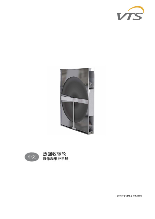
热回收转轮操作和维护手册DTR-VS-ver.5.0 (09.2017)IEC/EN 60439-1 +AC Low voltage switchgears and controllersVTS 保留非预先通知而修改的权利目录1. 介绍 (2)2. 技术数据 (3)2.1. 驱动单元基本参数 (3)2.1.1. 结构 (3)2.1.2. 驱动器操作 (3)2.2. 技术规范 (4)2.2.1. 结构 (4)2.2.2. 操作参数 (4)2.2.3. 元器件的额定参数 (4)2.3. 驱动单元的安装和配置 (5)2.4. 含变频器和VTS自控的驱动单元安装和配置 (5)2.4.1. 热回收转轮驱动回路的接线图 (5)2.4.2. 驱动单元的安装和配置 (6)2.4.3. 电机防护 (7)2.5. 自控系统的驱动单元安装和配置 (7)2.5.1. 热回收转轮驱动回路的接线图 (7)2.5.2. 热回收转轮驱动单元的控制 (8)2.5.3. 变频器配置例子 (8)2.5.4. 电机保护 (9)2.6. 系统中带有EC调速器的驱动单元安装和配置 (10)2.6.1. EC调节器的ModBus RTU/RS485参数 (11)2.6.2. 通过MODBUS设置旋转速度 (12)2.7. 安装建议 (13)3. 保存和运输 (14)4. 启动 (14)5. 维护 (15)5.1. 热回收转轮和驱动皮带 (15)5.2. 转轮密封 (16)1. 介绍本文档描述了关于热回收转轮的参数、运输、保管和服务内容。
●在进行任何动作前,务必详细阅读本文档。
2. 技术数据2.1. 驱动单元基本参数2.1.1. 结构本驱动单元是每个热回收转轮的完整部件。
基本构成如下:●变频器/EC电机控制器(取决于不同的版本或区域)●热回收轮芯●轮芯驱动皮带传动装置●电机减速器-马达带有减速齿轮2.1.2. 驱动器操作驱动单元用于启动并平缓地控制热回收转轮,使得速度在3-10rpm范围内。
品牌:Honeywell 产品名:HMR3000 型号:HHMR3000 品牌型号说明书

Digital Compass Solution HMR3000The Honeywell HMR3000 is a digital compass module that provides heading, pitch, and roll outputs for navigation. Three Honeywell’s magneto -resistive sensors are oriented in orthogonal directions to measure the vector components of earth’s magnetic field. A fluid tilt sensor is employed to determine a gravitational reference. These solid-state sensors create a strapdown compass that is both rugged and reliable. The data output is serial full-duplex RS-232 or half-duplex RS-485 with 1200 to 19,200 data rates.Applications include: Compassing & Navigation, Dead Reckoning Backup to GPS Systems, Marine Navigation, Antenna Positioning, and Land SurveyingA RS-232 development kit version is available that includes a windows compatible demo program (does not work with RS-485 devices), interface cable, AC adapter and carrying case.Honeywell continues to maintain product excellence and performance by introducing innovative solid-state magnetic sensor solutions. These are highly reliable, top performance products that are delivered when promised. Honeywell’s magnetic sensor solutions provide real solutions you can count on.FEATURES & BENEFITS BLOCK DIAGRAMHigh Accuracy, <0.5° with 0.1° ResolutionWide Tilt Range of ±40° Up to 20 Updates per Second NMEA Standard Sentence Outputs Hard Iron Calibration RoutineRS-232 or RS-485 Serial Data Interfaces PCB or Aluminum Enclosure Options6-15 volt DC Unregulated Power SupplyInterfaceHMR3000SPECIFICATIONSPower SupplyTemperature(2) Tested at 25°C except stated otherwise.(3) Characterized(4) Parts stationary for 24 hours before testing(5) The HMR3000 Demo Kit is not available with the RS-485 interface because the software does not support half-duplex protocol2 HMR3000 3PIN CONFIGURATION(1) Power input shall only be applied to either Pin 8 (+5VDC) or Pin 9 (Unregulated +6 to+15VDC).(2) Exceeding the voltage specifications for Pin 8 may damage the HMR3000.RS-232 UNBALANCED I/O INTERCONNECTSRS-485 BALANCED I/O INTERCONNECTSHMR3000HOST PCHOST PCHMR3000HMR3000DATA COMMUNICATIONSThe HMR3000 serial communications are governed by a simple asynchronous, ASCII protocol modeled after the NMEA0183 standard. Either an RS-232 or an RS-485 electrical interface can be ordered. ASCII characters are transmitted and received using 1 start bit, 8 data bits (LSB first), no parity (MSB always 0), and 1 stop bit; 10 bits total per character. Thebaud rate defaults to 19,200 and can be reconfigured to 1200, 2400, 4800, 9600, 19200, 38400 bits per second. TheHMR3000 supports both standard NMEA 0183 and proprietary messages. Unsolicited NMEA messages are sent by theHMR3000 in Continuous Mode at the rates programmed in the EEPROM. HMR3000 also responds to all input messagesfrom the host. An HMR3000 response to a command input may be delayed due to transmission of an unsolicited output.The host computer must wait for HMR3000 to respond to the last command input before sending another command message. All communication from and to HMR3000 contain a two-character Checksum Field at the end of the data fields,and are denoted in the sentences by ‘hh’. The checksum assures the accuracy of the message transmitted. This checksumis also calculated per NMEA 0183 Standard.The RS-232 signals are single-ended undirectional levels that are sent received simultaneously (full duplex). One signal isfrom the host personal computer (PC) transmit (TD) to the HMR3000 receive (RD) data line, and the other is from theHMR3000 TD to the PC RD data line. When a logic one is sent, either the TD or RD line will drive to about +6 Volts referenced to ground. For a logic zero, the TD or RD line will drive to about –6 Volts below ground. Since the signals are transmitted and dependent on an absolute voltage level, this limits the distance of transmission due to line noise and signalto about 60 feet.When using RS-485(1), the signals are balanced differential transmissions sharing the same lines (half-duplex). This meansthat logic one the transmitting end will drive the B line at least 1.5 Volts higher than the A line. For a logic zero, the transmitting end will drive the B line at least 1.5 Volts lower than the A line. Since the signals are transmitted as difference voltage level, these signals can withstand high noise environments or over very long distances where line loss may be a problem; up to 4000 feet. Note that long RS-485 lines should be terminated at both ends with 120-ohm resistors.Specific measurement descriptions and interface commands are not included in this datasheet but are included in the companion HMR3000 User’s Guide document.(1) Demonstration software for the HMR3000 does not support the RS-485(half-duplex) protocol. The software is onlyavailable with the RS-232 interface.CIRCUIT DESCRIPTIONThe HMR3000 Digital Compass Module contains all the basic sensors and electronics to provide digital indication of headingand tilt. The HMR3000 has all three axis of magnetic sensors on the far end of the printed circuit board, away from the connector interface. The HMR3000 uses the circuit board mounting holes or the enclosure surfaces as the reference mechanical directions. The complete HMR3000 PCB assembly consists of a mother board and the 9-pin D-connector.The HMR3000 circuit starts with the Honeywell HMC1001 1-Axis Magnetic Sensor and the HMC1002 2-Axis Magnetic Sensor elements to provide the X, Y, and Z axis magnetic sensing of the earth’s field. These sensor output voltages arethen amplfied and converted to a digital representation. A microcontroller integrated circuit receives the digitized magneticfield values (readings) by periodically querying the Analog to Digital Converter (ADC) and performs the necessary offsetvalue corrections provided by the EEPROM via the calibration routine. This microcontroller also performs the external serialdata interface and other housekeeping functions. The onboard EEPROM integrated circuit also is employed to retain necessary setup variables for best performance.A liquid filled two-axis (pitch, roll) tilt sensor is also used to create tilt compensated heading data. This tilt sensor performsan electronic gimballing function and is normally mounted flat (PCB horizontal) for maximum tilt range.4 HMR3000APPLICATIONS PRECAUTIONSSeveral precautions should be observed when using magnetic compasses in general:∙The presence of ferrous materials, such as nickel, iron, steel, and cobalt near the magnetometer will create disturbances in the earth’s magnetic field that will distort the X, Y, and Z field measurements.∙Perming effects on the HMR3000 circuit board need to be taken into account. If the HMR3000 is exposed to fields greater than 10 gauss, then it is recommended that the enclosure/circuit boards be degaussed for highestsensitivity and resolution. A possible result of perming is a high zero-field output indication that exceedsspecification limits. Degaussing wands are readily available from local electronics tool suppliers and areinexpensive. Severe field offset values could result if not degaussed.NON-FERROUS MATERIALSMaterials that do not affect surrounding magnetic fields are: copper, brass, gold, aluminum, some stainless steels, silver,tin, silicon, and most non-metals.HANDLING PRECAUTIONSThe HMR3000 Digital Compass Module measures fields within 1 gauss in magnitude. Computer floppy disks (diskettes)store data with field strengths of approximately 10 gauss. This means that the HMR3000 is many times more sensitive than common floppy disks. Please treat the compass with at least the same caution as your diskettes by avoiding motors, CRTvideo monitors, and magnets. Even though the loss of performance is recoverable, these magnetic sources will interferewith measurements.The fluidic tilt sensor works best when kept near level, and in calm to moderate vibration conditions. If turned upside downor violently jarred, not all the fluid will immediately return to the bottom of the tilt sensor’s glass ampoule. Accurate til t andtilt compensated headings may be unavailable for a minute or two to allow for the fluid to transit to the bottom of the ampoule.PCB DIMENSIONS AND PINOUT 5HMR30006 CASE DIMENSIONSDEMONSTRATION PCB MODULE KITThe HMR3000 Demonstration Kit includes additional hardware and Windows software to form a development kit for the digital compass module. This kit includes the HMR3000 PCB and enclosure, serial port cable with attached AC adapter power supply, and demo software plus documentation on a compact disk (CD). The figure below shows the schematic of the serial port cable with integral AC adapter. There will be three rotary switches on the AC adapter. These should be pointed towards the positive (+) polarity, +9 volts, and 120 or 240 VAC; depending your domestic supply of power.22D9-FD9-F359359HMR3000 7ORDERING INFORMATIONFIND OUT MOREFor more information on Honeywell’s Magnetic Sensors visit us online at .The application circuits herein constitute typical usage and interface of Honeywell product. Honeywell does not warranty or assume liability of customer-designed circuits derived from this description or depiction.Honeywell reserves the right to make changes to improve reliability, function or design. Honeywell does not assume any liability arising out of the application or use of any product or circuit described herein; neither does it convey any license under its patent rights nor the rights of others.U.S. Patents 4,441,072, 4,533,872, 4,569,742, 4,681,812, 4,847,584 and 6,529,114 apply to the technology describedPDS-42005September 2015©2015 Honeywell International Inc.Honeywell12001 Highway 55 Plymouth, MN 55441。
超特克HV9961DB1高亮LED驱动板说明书

Supertex inc.HV9961DB190-265VAC50/60Hz0 -1.5V for LD function or leave openGeneral DescriptionThe HV9961 demoboard is a high-brightness LED driver employing the patent-pending average-mode constant current control scheme by Supertex Inc. The power conversion stage of the HV9961DB1 consists of a diode bridge rectifier followed by a buck converter operating with fixed off-time of 20µs.The HV9961DB1 LED driver features tight regulation of the LED current within a few milliamps over the entire rangeof the input AC line and the output LED string voltage. The LED current accuracy is almost insensitive to the passive component tolerances, such as the output filter inductance or the timing resistor. The accuracy of the LED current is mainly determined by the internal 275mV ± 3% referencevoltage of the HV9961 control IC and by the external current sense resistor tolerance. The output current can be adjusted down to 60mA using an on-board potentiometer. However, the accurate current control is only achieved with continuous conduction of the filter inductor, i.e. when the LED current is greater than the inductor ripple current amplitude. (Note, that the linear dimming input of the HV9961 disables switching, when its voltage falls below a 200V threshold. Expect the LED driver to shut off when the LED current falls below 50 ~ 55mA.)PWM dimming can be achieved by applying a pulse-width-modulated square wave signal between the PWMD andGND pins.The HV9961DB1 features protection from an output short circuit condition. Open LED protection is inherent, since the output filter capacitor can accept the full rated rectified AC line voltage. Please, note that the demoboard is not CISPR15 compliant. An additional input EMI filter circuit is required to make the board meet conducted electro-magnetic emission limits. Also, note that:NO SAFETY ISOLATION OF THE LED LOADFROM THE AC MAINS VOLTAGE IS PROVIDED!21-Watt Universal AC LED Driver Demoboard with Accurate Average-Mode Constant Current ControlConnection DiagramWARNINGDo not connect earth-grounded test instruments. Doing so will short the AC line, resulting in damage to the instrument and/or the HV9961DB1. Use floating high voltage differential probes or isolate the demoboard by usingan isolating transformer.WARNINGNo galvanic isolation.Dangerous voltages are present when connected to the AC line.1. Connect the input AC voltage between the AC INterminals as shown in the connection diagram.2. Connect the LED string between LED+ (anode ofLED string) and LED- (cathode of LED string).3. Connect the PWMD terminal to the VDD terminalusing the jumper provided to enable the LED driver.4. The current level can be adjusted by applying 0 -1.5V between LD and GND. Leave LD floating to use the internal current setting.ConnectionsPWM DimmingThe HV9961DB1 is capable of being PWM dimmed by ap-plying a square wave TTL compatible signal between PWMD and GND terminals. However, since there is no galvanic iso-lation on the board, care must be taken to prevent damage to the PWM dimming source and/or the HV9961DB1. One simple way is to isolate the LED driver from the AC line using an isolation transformer. Another approach is to use an opto-isolator to drive the PWMD pin as shown in the figure below.5.0Vsquarewavesignal(<1.0kHz)PWMDVDD(e.g. LTV-814 from Lite-On)L E D C u r r e n t (A )AC Line Voltage (VAC)AC Line Voltage (VAC)0.3620.3600.3580.3560.3540.3520.3500.3480.346L E D C u r r e n t (A )PWM Dimming Response Short Circuit CurrentI LEDPWMDV IN = 240VAC0.3400.3450.3550.3600.3650.370Typical CharacteristicsSchematicJ3B J3C Silk ScreenSupertex inc. does not recommend the use of its products in life support applications, and will not knowingly sell them for use in such applications unless it receives an adequate “product liability indemnification insurance agreement.” Supertex inc. does not assume responsibility for use of devices described, and limits its liability to the replacement of the devices determined defective due to workmanship. No responsibility is assumed for possible omissions and inaccuracies. Circuitry and specifications are subject to change without notice. For the latest product specifications refer to the Supertex inc. (website: http//)©2013 Supertex inc.All rights reserved. Unauthorized use or reproduction is prohibited.Supertex inc.。
和谐XPS安全自动化产品数据表说明书

Product data sheetSpecificationsTime delayed output, Harmony XPS,for Estop, guard, OSSD, 24 V AC/DC, springXPSBAT12A1ACMainRange of ProductHarmony Safety Automation Product or Component Type Safety module Safety module name XPSBATSafety module application For emergency stop and protective guard applications For OSSD monitoringFunction of moduleEmergency stop button with 2 NC contacts Guard monitoring with 1 or 2 limit switches Light curtain monitoring RFID switchMonitoring of electro-sensitive protection equipment (ESPE)Safety levelCan reach PL e/category 4 for normally open relay contact ISO 13849-1Can reach SILCL 3 for normally open relay contact IEC 62061Can reach SIL 3 for normally open relay contact IEC 61508Can reach PL c/category 1 for normally closed relay contact ISO 13849-1Can reach SILCL 1 for normally closed relay contact IEC 62061Can reach SIL 1 for normally closed relay contact IEC 61508Safety reliability dataMTTFd > 30 years ISO 13849-1Dcavg >= 99 % ISO 13849-1PFHd = 0.98E-09 for SS0 ISO 13849-1PFHd = 0.96E-09 for SS1 ISO 13849-1HFT = 1 IEC 62061PFHd = 0.98E-09 for SS0 IEC 62061PFHd = 0.96E-09 for SS1 IEC 62061SFF > 99% IEC 62061HFT = 1 IEC 61508-1PFHd = 0.98E-09 for SS0 IEC 61508-1PFHd = 0.96E-09 for SS1 IEC 61508-1SFF > 99% IEC 61508-1Type = B IEC 61508-1Electrical circuit type NC pair OSSD pairConnections - terminalsRemovable spring terminal block, 0.2...2.5 mm² solid or flexibleRemovable spring terminal block, 0.25...2.5 mm² flexible with ferrule single conductor Removable spring terminal block, 0.2...1.5 mm² solid or flexible twin conductorRemovable spring terminal block, 2 x 0.25...1 mm² flexible with ferrule without cable end, with bezel Removable spring terminal block, 2 x 0.5...1.5 mm² flexible with ferrule with cable end, with bezel [Us] Rated Supply Voltage24 V AC - 15...10 %24 V DC - 20...20 %ComplementarySynchronisation time between inputs 0.5 s 2 sType of startAutomatic/manual/monitored Power consumption in W2 W 24 V DCD i s c l a i m e r : T h i s d o c u m e n t a t i o n i s n o t i n t e n d e d a s a s u b s t i t u t e f o r a n d i s n o t t o b e u s e d f o r d e t e r m i n i n g s u i t a b i l i t y o r r e l i a b i l i t y o f t h e s e p r o d u c t s f o r s p e c i f i c u s e r a p p l i c a t i o n sPower consumption in VA5 VA 24 V AC 50/60 HzInput protection type Internal, electronicSafety outputs 2 NO1 NOSafety inputs2Maximum wire resistance500 OhmTime delay range0...900 sInput compatibility Normally closed circuit ISO 14119Mechanical contact ISO 14119OSSD pair IEC 61496-1-2Normally closed circuit ISO 138503-wire proximity sensors PNP[Ie] rated operational current5 A AC-13 A AC-155 A DC-13 A DC-13Control outputs 3 pulsed outputInput/Output type Semiconductor output Z1, 20 mA[Ith] conventional free air12 Athermal currentAssociated fuse rating6 A gG NO relay output circuit IEC 60947-1 Minimum output current20 mA relay outputMinimum output voltage24 V relay outputMaximum response time on20 msinput open[Ui] rated insulation voltage250 V 2)EN/IEC 60947-1[Uimp] rated impulse withstand4 kV II EN/IEC 60947-1voltageLocal signalling LED green power power ONLED red error errorLED yellow state 1 safety output instantaneousLED yellow state 2 safety output delayedLED yellow start 1 startLED yellow start 2 startLED yellow S12 safety input S12LED yellow S22 safety input S22Mounting Support35 mm symmetrical DIN railDepth 4.72 in (120 mm)Height 3.94 in (100 mm)Width 1.77 in (45 mm)Net Weight0.77 lb(US) (0.350 kg)EnvironmentStandards IEC 60947-5-1IEC 61508-1 functional safety standardIEC 61508-2 functional safety standardIEC 61508-3 functional safety standardIEC 61508-4 functional safety standardIEC 61508-5 functional safety standardIEC 61508-6 functional safety standardIEC 61508-7 functional safety standardISO 13849-1 functional safety standardIEC 62061 functional safety standardProduct certifications TÜVcULusIP degree of protection IP20 terminals)EN/IEC 60529IP40 housing)EN/IEC 60529IP54 mounting area)EN/IEC 60529 Ambient air temperature for-13…131 °F (-25…55 °C)operationAmbient Air Temperature for-13…185 °F (-25…85 °C)StorageRelative Humidity5…95 % non-condensingOrdering and shipping detailsCategory22477-SAFETY MODULES (PREVENTA)Discount Schedule SAF2GTIN3606482034037Nbr. of units in pkg.1Package weight(Lbs)10.65 oz (302 g)Returnability NoPacking UnitsUnit Type of Package 1PCEPackage 1 Height 2.52 in (6.4 cm)Package 1 width 5.24 in (13.3 cm)Package 1 Length 6.02 in (15.3 cm)Unit Type of Package 2S03Number of Units in Package 216Package 2 Weight11.92 lb(US) (5.409 kg)Package 2 Height11.81 in (30 cm)Package 2 width11.81 in (30 cm)Package 2 Length15.75 in (40 cm)Package 3 Height11.81 in (30 cm)Offer SustainabilitySustainable offer status Green Premium productCalifornia proposition 65WARNING: This product can expose you to chemicals including: Lead and lead compounds, which isknown to the State of California to cause cancer and birth defects or other reproductive harm. For moreinformation go to REACh Regulation REACh DeclarationEU RoHS Directive Pro-active compliance (Product out of EU RoHS legal scope)EU RoHS DeclarationMercury free YesRoHS exemption information YesChina RoHS Regulation China RoHS declarationEnvironmental Disclosure Product Environmental ProfileCircularity Profile End of Life InformationWEEE The product must be disposed on European Union markets following specific waste collection andnever end up in rubbish bins.Dimensions Drawings DimensionsFront and Side Views(A) : Product drawing(B) : Spring terminal(C) : Side view(1) : Removable terminal blocks, top(2) : Removable terminal blocks, bottom(3) : LED indicators(4) : Delay factor selector(5) : Delay base selector(6) : Sealable transparent coverMounting to DIN railScrew-mountingConnections and SchemaWiring Diagram(1) : A1-A2 (Power supply)(2) : S11–S21 (Control outputs (DC+) of safety-related inputs), S12-S22 (Input channels (CH+) of safety-related inputs)(3) : Y1 (Control output of Start/Restart input), Y2 (Input channel for automatic/manual start), Y3 (Input channel for monitored start with falling edge)13-14-23-24 : Terminals of the safety-related outputs (instantaneous)37-38 : Terminals of the safety-related outputs (delayed)Z1 : Solid state output, not safety-related。
艾顿072907 电源保护设备说明书

Eaton 072907Eaton Moeller® series E-PKZ0 Insulated enclosure, E-PKZ0, H x W x D = 129 x 85 x 124 mm, flush-mounted, rotary handle, black/gray, IP55General specificationsEaton Moeller® series E-PKZ0 Accessory Insulated enclosure0729074015080729075124 mm 129 mm 85 mm 0.224 kgIEC/EN 60947-4-1 CSA Class No.: 3211-05 CSA-C22.2 No. 14 CECSA File No.: 165628 UL UL 508UL Category Control No.: NLRV UL File No.: E36332 CSAProduct NameCatalog Number EANProduct Length/Depth Product Height Product Width Product Weight Certifications0 AAccessoriesIs the panel builder's responsibility. The specifications for the switchgear must be observed.0 W0 WMeets the product standard's requirements.Is the panel builder's responsibility. The specifications for the switchgear must be observed.Does not apply, since the entire switchgear needs to be evaluated.Meets the product standard's requirements.Black-gray rotary knobPE(N) terminalNEMA 1NEMA 12IP55NEMA 3RMeets the product standard's requirements.Meets the product standard's requirements.Is the panel builder's responsibility.eaton-manual-motor-starters-mounting-e-pkz0-accessory-dimensions.eps eaton-manual-motor-starters-enclosure-e-pkz0-accessory-dimensions-002.epseaton-manual-motor-starters-enclosure-e-pkz0-accessory-dimensions-003.epseaton-manual-motor-starters-enclosure-e-pkz0-accessory-dimensions.eps eaton-manual-motor-starters-enclosure-e-pkz0-accessory-3d-drawing-003.epsDA-CE-ETN.E-PKZ0-GIL03402029ZDA-CD-e_pkz0_gDA-CS-e_pkz0_gRated operational current for specified heat dissipation (In) Product category10.11 Short-circuit ratingEquipment heat dissipation, current-dependent PvidHeat dissipation capacity Pdiss10.4 Clearances and creepage distances10.12 Electromagnetic compatibility10.2.5 Lifting10.2.3.1 Verification of thermal stability of enclosuresFitted with:Degree of protection (front side)10.2.3.2 Verification of resistance of insulating materials to normal heat10.2.3.3 Resist. of insul. mat. to abnormal heat/fire by internal elect. effects10.8 Connections for external conductors10.9.2 Power-frequency electric strength DibujoseCAD model Instrucciones de instalación mCAD modelIs the panel builder's responsibility.Degree of protectionIP55NEMA OtherAmbient operating temperature - max40 °C10.7 Internal electrical circuits and connectionsIs the panel builder's responsibility.10.10 Temperature riseThe panel builder is responsible for the temperature rise calculation. Eaton will provide heat dissipation data for the devices.Static heat dissipation, non-current-dependent Pvs0 W10.9.3 Impulse withstand voltageIs the panel builder's responsibility.Enclosure materialPlasticAmbient operating temperature - min-25 °C10.2.2 Corrosion resistanceMeets the product standard's requirements.10.6 Incorporation of switching devices and componentsDoes not apply, since the entire switchgear needs to be evaluated.10.2.4 Resistance to ultra-violet (UV) radiationPlease enquire10.2.7 InscriptionsMeets the product standard's requirements.10.5 Protection against electric shockDoes not apply, since the entire switchgear needs to be evaluated.ModelBuilt-in10.13 Mechanical functionThe device meets the requirements, provided the information in the instruction leaflet (IL) is observed.10.2.6 Mechanical impactDoes not apply, since the entire switchgear needs to beEaton Corporation plc Eaton House30 Pembroke Road Dublin 4, Ireland © 2023 Eaton. Todos los derechos reservados. Eaton is a registered trademark.All other trademarks areproperty of their respectiveowners./socialmediaevaluated.Is the panel builder's responsibility.Does not apply, since the entire switchgear needs to be evaluated.0 W10.9.4 Testing of enclosures made of insulating material 10.3 Degree of protection of assembliesHeat dissipation per pole, current-dependent Pvid。
MP2451 数据手册

PACKAGE REFERENCE
TOP VIEW BST GND FB 1 2 3 6 5 4 SW VIN EN
ABSOLUTE MAXIMUM RATINGS (1)
Supply Voltage (VIN).......................–0.3V to 40V Switch Voltage (VSW)....... –0.3V to VIN (MAX)+0.3V BST to SW ....................................... -0.3 to 6.0V All Other Pins ................................–0.3V to 5.0V (2) Continuous Power Dissipation (TA=+25°C) ........................................................... 0.57W Junction Temperature ...............................150°C Lead Temperature ....................................260°C Storage Temperature................. -65°C to 150°C
Pin # 1 2 3 4 5 6 Name BST GND FB EN VIN SW Description Bootstrap. This is the positive power supply for the internal floating high side MOSFET driver. Connect a bypass capacitor between this pin and SW pin. Ground. It should be connected as close as possible to the output capacitor avoiding the high current switch paths. Feedback. This is the input to the error amplifier. An external resistive divider connected between the output and GND is compared to the internal +0.8V reference to set the regulation voltage. Enable input. Pulling this pin below the specified threshold shuts the chip down. Pulling it above the specified threshold enables the chip. Floating this pin shuts the chip down. Input Supply. This supplies power to all the internal control circuitry, both BS regulators and the high side switch. A decoupling capacitor to ground is required close to this pin to reduce switching spikes. Switch node. This is the output from the high-side switch. A low VF Schottky diode to ground is required close to this pin to reduce switching spikes.
超特克LED驱动演示板HV9930DB1说明书

Supertex inc.HV9930DB1General DescriptionThe HV9930DB1 is an LED driver demoboard capable of driving up to 7 1-watt LEDs in series from an automotive input of 9 - 16VDC. The demoboard uses Supertex’s HV9930 in a boost-buck topology. The converter operates at frequencies in excess of 300kHz and has excellent output current regulation over the input voltage range. It can also withstand transients up to 42V and operate down to 6V input. The converter is also protected against open LED and output short circuit conditions. Protection against reverse polarity up to 20V is also included.Board Layout and Connection DiagramHigh Bright LED Driver IC DemoboardMeeting Automotive RequirementsConnections:Input - The input is connected between the terminals of connector J1 as shown in the Connection Diagram.Output - The output is connected between the terminals of connector J2 as shown.Enable/PWM Dimming:To just enable the board, short pins 1 and 2 of connector J3 as shown. For PWM dimming, connect the external push-pullsquare wave source between terminals 1 and 3 of connectorJ3 as shown by the dotted lines.Note: During PWM dimming, pin 2 of connector J3 should be left open. Also, the PWM signal must have the proper polarity with the positive connected to pin 1 of J3. Note that pin 3 of J3 is internally connected to the return path of the input voltage.Actual Size: 2.25” x 1.25”PWM DimmingV INTesting the Demo BoardNormal Operation: Connect the input source and the output LEDs as shown in the Connection Diagram and enable the board. The LEDs will glow with a steady intensity. Connect-ing an ammeter in series with the LEDs will allow measure-ment of the LED current. The current will be 350mA +/- 5%.Open LED test: Connect a voltmeter across the output ter-minals of the HV9930DB1. Start the demoboard normally, and once the LED current reaches steady state, unplug one end of the LED string from the demoboard. The output volt-age will rise to about 33V and stabilize.Short Circuit Test: When the HV9930DB1 is operating in steady state, connect a jumper across the terminals of the LED string. Notice that the switching frequency drops, but the average output current remains the same.PWM Dimming: With the input voltage to the board discon-nected, apply a TTL compatible, push-pull square wave sig-nal between PWMD and GND terminals of connector J3 as shown in the Connection Diagram. Turn the input voltage back on and adjust the duty cycle and / or frequency of the PWM dimming signal. The output current will track the PWMdimming signal. Note that although the converter operates perfectly well at 1.0kHz PWM dimming frequency, the best PWM dimming ratios can be obtained at lower frequencieslike 100 or 200HzTypical ResultsFig. 1 shows the efficiency plot f or the HV9930DB1 over the input voltage range. The converter has efficiencies greater than 80% over 13V input. Note that these measurements do not include the 0.3 - 0.5W loss in the reverse blocking diode.Fig. 2 shows the variation of the switching frequency over the input votage range. The frequency varies from 300kHz to 500kHz over the entire input voltage range and avoids the restricted frequency band of 150kHz to 300kHz and the AM band greater than 530kHz. This makes it easier to meet the conducted and radiated EMI specifications for the automo -tive industry.Fig.3 shows the output current variation over the input volt-age range. The LED current has a variation of about 2.0mA over the entire voltage range.7072747678808284Input Voltage (V)E f f i c i e n c y (%)300350400450500Input Voltage (V)S w i t c h i n g F r e q u e n c y (k H z )348.0348.5349.0349.5350.0350.5Input Voltage (V)O u t p u t C u r r e n t (m A )Fig. 3 Output Current vs. Input VoltageThe waveforms in Fig.4 show the drain voltage of the FET (channel 1 (blue); 10V/div) and the LED current (channel 4 (green); 100mA/div) at three different operating conditions – 9.0V in, 13.5V in and 16V in.Fig. 5 shows the operation of the converter during cold crank conditions as the input voltage decreases from 13.5V to 6V and increases back to 13.5V. In these cases, the input current reaches the limit set and the output current drops correspondingly. Thus, the LEDs continue to glow, but with reduced intensity. Once the voltage ramps back up, the out-put current goes back to its normal value and the converter comes out of the input current limit.Fig.6 shows the LED current during an input step change from 13.5 to 42V and back to 13.5V (similar to a clamped load dump). It can be seen that the LED current drops brieflywhen the input voltage jumps, but there are no overshoots.(a)(b)(c)Fig. 4. Steady State Waveforms(a): 9.0V in; (b): 13.5V in; (c): 16V inFig. 5. Cold Crank OperationChannel 1 (blue): Input voltage (10V/div)Channel 3 (pink): Input current (1A/div)Channel 4 (green): LED current; 100mA/divFig. 6 LED current during step changesin the input voltageChannel 1(blue): Input voltage (10V/div)Channel 4 (green): LED current (100mA/div)Fig. 7a shows the operation of the converter during an Open LED condition and Fig. 7b shows the operation during output short circuit condition. In both cases, it can be seen that the HV9930DB1 can easily withstand faults and come back into normal operation almost instantly.Fig. 8 shows the PWM dimming performance of the HV9930DB1 with a 100Hz, 3.3V square wave signal. The converter can easily operate at PWM dimming duty cyclesfrom 1% - 99%.(a): Open LED Condition(b): Output Short CircuitFig. 7 HV9930DB1 during output fault conditionsFET drain voltage (20V/div)Channel 1 in (a); Channel 2 in (b)Channel 4 (green): LED currentShort Circuit(a)(b)(c)Fig. 8 PWM Dimming at 100HzChannel 1 (blue): PWM Dimming Input Signal (2V/div)Channel 4 (Green): LED current (100mA/div)Fig. 9 shows the rise and fall times of the output current dur-ing PWM dimming. The converter has nearly symmetric rise and fall times of about 25µs. These rise and fall times can be reduced (if desired) by reducing the output capacitance C10. However, this will lead to increased ripple in the output current.Conducted EMI Tests on theHV9930DB1In preliminary tests conducted on the demo board, the board meets SAE J1113 Class 3 conducted EMI standards without the need for any input filters (other than the input capacitors already included). This is a result of the combination of the continuous input current and a localized switching loop (Q1 – C1 – D3).Table 1 details the conducted EMI limit as per SAE J1113 and the maximum conducted EMI obtained from measure-ments on the board. The table also lists the Class of the SAE standard the board meets in each frequency range.The conducted EMI plots for the HV9930DB1 obtained at an input voltage of 13.5V and an LED string voltage of 27V(output current is 350mA) are given in the Appendix. Fig. 9. PWM Dimming rise and fall timesChannel 1 (blue): PWM Dimming Input Signal (2V/div)Channel 4 (Green): LED current (100mA/div)(a): rise time(b): fall timeHV9930DB1 Circuit Schematic:PCB Top LayerPCB Bottom LayerAppendix – Conducted EMI Test ResultsAppendix – Conducted EMI Test Results (cont.)Ref. Level = 65dBµVRef. Level = 49dBµVSupertex inc. does not recommend the use of its products in life support applications, and will not knowingly sell them for use in such applications unless it receives an adequate “product liability indemnification insurance agreement.” Supertex inc. does not assume responsibility for use of devices described, and limits its liability to the replacement of the devices determined defective due to workmanship. No responsibility is assumed for possible omissions and inaccuracies. Circuitry and specifications are subject to change without notice. For the latest product specifications refer to the Supertex inc. (website: http//)©2013 Supertex inc.All rights reserved. Unauthorized use or reproduction is prohibited.Supertex inc.。
- 1、下载文档前请自行甄别文档内容的完整性,平台不提供额外的编辑、内容补充、找答案等附加服务。
- 2、"仅部分预览"的文档,不可在线预览部分如存在完整性等问题,可反馈申请退款(可完整预览的文档不适用该条件!)。
- 3、如文档侵犯您的权益,请联系客服反馈,我们会尽快为您处理(人工客服工作时间:9:00-18:30)。
ECP2459
4.5-60V 0.5A 480KHz Step-down converter in a SOT23-6
Preliminary v01 01/2020
Description
The ECP2459 is a monolithic,step-down, switch-mode converter with a built-in power MOSFET. It achieves a 0.5A peak-output current over a wide input supply range with excellent load and line regulation. Current- mode operation provides a fast transient response and eases loop stabilization. Fault condition protections include cycle-by-cycle current limiting and thermal shutdown. The ECP2459 requires a minimal number of readily available, external components and is available in a space saving SOT23-6 package.Feature
Input voltage range : 4.5V~60V
0.5A peak output current
1Ω Internal power MOSFET
Fixed 480KHz frequency
Up to 90% efficiency
1μA shutdown mode
Package Type : SOT23-6 Application
Power meters
Distributed power systems
Industrial power systems
B attery chargers
Pre-regulator for linear regulators
Functional Block Diagram Typical Application
Description
Bootstrap pin for top switch. A 0.1uF or larger capacitor should be connected between this pin and the SW pin to supply current to the top switch and top switch driver.
Ground pin.
Output feedback pin. Input to the error amplifier.Set the output voltage.When the load is short-circuited, FB voltage is lower than 250mV, the return circuit will reduce the oscillation
Typical Characteristics V IN=12V, unless otherwise noted.
VIN=12V, VOUT=5V, L=10μH, TA=25°C, unless otherwise noted.
VIN=12V, VOUT=5V, L=10μH, TA=25°C, unless otherwise noted.
Application Information
Setting Output Voltage
The external resistor divider sets the output voltage (see the Typical Application schematic). Table 1 lists resistors for common output voltages. The feedback resistor (R2) also sets the feedback loop bandwidth with the internal compensation network (see Figure 1). R1 is:
PCB Layout Guide
PCB layout is very important to stability. Please follow these guidelines and use Figure 1 as reference.
1)Keep the path of switching current short and minimize the loop area formed by the input
capacitor, high-side MOSFET, and Schottky diode.
2)Keep the connection from the power ground →Schottky diode→SW pin as short and wide as
possible.
3)Ensure all feedback connections are short and direct. Place the feedback resistors and
compensation components as close to the chip as possible.
4)Route SW away from sensitive analog areas such as FB.
5)Connect IN, SW, and especially GND to large copper areas to cool the chip for improved
thermal performance and longterm reliability. For single layer PCBs, avoid soldering the exposed pad.
Figure 1:PCB Layout
Typical Application Circuit
Figure 3: 5V Output Typical Application Circuit:
Figure 4: 3.3V Output Typical Application Circuit
ECP2459
Package Information
SOT23-6
Note:
1. All dimensions are in millimeters.
2. Package length does not include mold flash, protrusion or gate burr.
3.
Package width does not include flash or protrusion.
4. Lead coplanarity (bottom of leads after forming) shall be 0.10 millimeters max.
5. Pin 1 is lower left pin when reading top mark from left to right.。