以AT89C2051单片机为控制核心的数字温度计设计
基于AT89C2051数字温度计的设计

、I
一
整 流 , 波 滤
! 竺 l
数 码 管 显 示 温 度
l买 l
CD 5 1 4 1
(T 925 ) A 8 C 0 1
( 8 5 稳 压 70)
译 码 器
根 据 F与温 度 的 对 应关 系 ,
转 驺 换 一
编 程求 温 度 值
收 稿 日期 :0 2 0 ~ 0 2 1— 4 2
通讯作者 : 陈石龙 (9 4 )男 , 18 一 , 助理工程师.E m i 1 15 16 qcm — a :2 45 3 @q . l o
第 2期
陈石龙 : 基于A 9 2 5 数字 温度计 的设计 T8 C 0 1
・ l9 ・ 7
的电源输入是否为1V 2 左右 , 检查A 8 c 0 lC 4 1的电源输入是否为5 左右 , T 9 2 5 ,D 5 1 V 表示能正常工作.
.
( 下转 第1 1 ) 9页
第 2期
王
明 : ] a a 工上班时间记录系统 的设计 基=J v 员 =
J v - a e mp o e i e o d n y tm a a b sd e ly e tme r c r i g s se
图4 M 3内部结构图 L 31
R = . , = 0u 所Il t - 11 Z 可得频率每升高2H , 2 6 k c 0 1 , ) o : 2 1H , 8 2 . u0  ̄ 1 Z 温度升高一度. 子程序流程如图6 所示
N
图5 中断程序流程 图
图6 频率转换温度算法程序流程
5 调试 过程与 注意事项
}
厂
\
AT89C51单片机数字体温计的设计

机 系 统 对 输 入 的 信 号 进 行 处 理 , 成 显 示 码 送 往 液 形 晶显 示 模 块 R 6 2 显 示 , 成 温 度 从 采 集 、 据 T1 O C 完 数 处 理 到 数 字 显 示 的 整 体 功 能 。 图 2为 硬 件 实 物 图 。
单 片机来 设计 数字 体温计 。但 由于单 片机 的接 口信 号 是数字 信号 , 想 使用 单 片机 来 处 理体 温 这 类 非 若 电信号 , 必须 借助 于温 度传感 器 , 将温 度转 换成 弱 的
数 字体 温计 与普 通 的水银 体 温计相 比 , 有测 温 时 间短 、 围广 、 具 范 读数 准确 和 方便 显 示等 优 点 。整 个设 计 系统 简单 , 操作 灵 活 , 可编程 度非 常 高。
关 键 词 AT8 C5 ; 1 B2 数 字 体 温 计 9 1 DS 8 0;
本 设 计 在 软 件 方 面采 用 Ke — C 1 片 机 C语 i l 5单
+ 15 。 2 ℃
DS 8 2 1 B 0温 度 测 量 工 作 过 程 , 要 是 通 过 计 数 主 器 计 数 一 个 由温 度 系 数 较 低 的 晶 振 在 当 前 温 度 条 件
言设计 , 定程 度上 简化 了软 件编 写 , 一 而且逻 辑性更 强 , 低 了程序 在运 行 过 程 中出 现死 循 环 和 跑 飞 的 降
个单 线接 口发送 和接 收 信 号 , 单 片机 之 间 仅需 和
条 连 接 线 ( 上 电线 ) 无 需A/ 加 , D转 换 , 且 读 写 而
一
收 稿 日期 :0 20 7 2 1-82
修 回 日期 :o 20 一 l 2 1 — 9 O
作 者 简 介 : 文 祥 (9 3 )男 , 曹 1 8 ~ , 助教 . — i C @wg y n t E mal WX : x . e
基于DS1620和AT89C2051的数字温度计的设计

基于DS1620和AT89C2051的数字温度计的设计DS1620是一片8引脚的片内建有温度测量并转换为数字值的,他集温度传感、温度数据转换与传输、温度控制等功能于一体。
测温范围:-55~+125℃,精度为0.5℃。
该芯片十分简单与衔接,实现温度的测控应用,单独做温度控制器用法时,可不用外加其他辅助元件。
引脚功能及罗列1所示。
其中:RST,CLK/CONV及DQ为三线串行通信线;DQ为数据输入输出端。
当RST保持高电平,对应CLK/CONV时钟脉冲的升高沿处,DQ可按位输入各种控制命令及数据,在CLK/CONV时钟脉冲的下降沿处开头按位输出9 B温度值,分2个字节输出,最低位(LSB)在最先输出,先输出的1个字节(8 B)除以2就是摄氏温度值,后输出的1个字节(仅1 B)为温度的符号位,是0为正,是1为负。
RST为低电平常结束通信,CLK/CONV保持低电平,DQ展现高阻态,但芯片内部在举行温度的测量与数字转换(即温度值的更新),这需要大约1 s的时光。
引脚THIGH为高温临界触发输出端,当所测温度高于高温临界寄存器中设定的温度TH时,该引脚由低电平变为高电平,而温度低于TH时又回到低电平;TLOW为低温临界触发输出端,其电平变幻与THIGH类似;TCOM为高/低温临界组合触发输出端;他们都可作为温度调整器的输出端,挺直控制加热或冷却设备。
DS1620内部有一个工作方式寄存器,如表1所示。
其中:DONE为温度数据转换位,为0时表示正,在转换过程中,为1表示已转换完毕;THF:高温标记位,当温度高于或等于高温临界寄存器中的设定值TH时,硬件对该位置位,但硬件不能对该位清零;TLF:
第1页共3页。
(完整word版)基于AT89C51单片机数字温度计的设计

基于AT89C51单片机数字温度计的设计一、项目概述在生活和生产中,人们经常要用到一些测温设备,但是传统的测温设备具有制作成本高、硬件电路和软件设计复杂登缺点。
基于AT89C51的数字温度计具有制作简单、成本低、读数方便、测温范围广等优点,应用前景广泛。
二、项目要求基于AT89C51的数字温度计的具体要求如下:1.温度值用LED显示。
2.测温范围为-30~100℃,且测量误差不大于±0.5℃。
3.成品的体积、质量尽可能小。
三、设计框图及流程图1 主控制器单片机AT89S51具有低电压供电和体积小等特点,四个端口只需要两个口就能满足电路系统的设计需要,很适合便携手持式产品的设计使用系统可用二节电池供电。
2 显示电路显示电路采用4位共阳LED数码管。
3温度传感器DS18B20温度传感器是美国DALLAS半导体公司最新推出的一种改进型智能温度传感器,与传统的热敏电阻等测温元件相比,它能直接读出被测温度,并且可根据实际要求通过简单的编程实现9~12位的数字值读数方式。
DS18B20的性能特点如下:●独特的单线接口仅需要一个端口引脚进行通信;●多个DS18B20可以并联在惟一的三线上,实现多点组网功能;●无须外部器件;●可通过数据线供电,电压范围为3.0~5.5V;●零待机功耗;●温度以9或12位数字;●用户可定义报警设置;●报警搜索命令识别并标志超过程序限定温度(温度报警条件)的器件; ●负电压特性,电源极性接反时,温度计不会因发热而烧毁,但不能正常工作;DS18B20采用3脚PR -35封装或8脚SOIC 封装,其内部结构框图如下图所控制器使用单片机AT89C51,测温传感器使用DS1820,用4位共阳极LED 数码管以动态扫描法实现温度显示,电路图如图1所示:图1.电路原理图五、软件设计1.程序流程图主程序的主要是负责温度的实时显示,读出并处理DS1280测量的当前温度值,温度测量每1s进行一次。
毕业设计(论文)-基于at89c51单片机的简易数字温度计的设计[管理资料]
![毕业设计(论文)-基于at89c51单片机的简易数字温度计的设计[管理资料]](https://img.taocdn.com/s3/m/0e7fceff76c66137ef061979.png)
GND:接地。
P0口:P0口为一个8位漏级开路双向I/O口,每脚可吸收8TTL门电流。当P0口的管脚第一次写1时,被定义为高阻输入。P0能够用于外部程序数据存储器,它可以被定义为数据/地址的第八位。在FIASH编程时,P0口作为原码输入口,当FIASH进行校验时,P0输出原码,此时P0外部必须被拉高。
A
与MCS-51兼容;
4K字节可编程闪烁存储器;
寿命:1000写/擦循环;
数据保留时间:10年;
全静态工作:0Hz-24MHz;
三级程序存储器锁定;
128×8位内部RAM;
32可编程I/O线;
两个16位定时器/计数器;
5个中断源。
A
其引脚排列如图3-1所示:
各引脚功能简单介绍如下:
VCC:供电电压。
[Key words]digital thermometer; DS18B20; AT89C51;alarm.
现代社会对各种信息参数的准确度和精确度的要求都有了几何级的增长,而如何准确而又迅速的获得这些参数就需要受制于现代信息基础的发展水平。在三大信息信息采集(即传感器技术)、信息传输(通信技术)和信息处理(计算机技术)中,传感器属于信息技术的前沿尖端产品,尤其是温度传感器技术,在我国各领域已经引用的非常广泛,可以说是渗透到社会的每一个领域,人民的生活与环境的温度息息相关,在工业生产过程中需要实时测量温度,在农业生产中也离不开温度的测量,因此研究温度的测量方法和装置具有重要的意义。
基于AT89C2051的数字温度计设计
基于AT89C2051的数字温度计设计作者:周学军来源:《现代电子技术》2010年第17期摘要:利用单片机AT89C2051作为控制器,以及用改进型智能温度传感器DS18B20作为温度采集器,设计了一款数字温度计。
该数字温度计能够测出-55~+125 ℃之间的温度,与传统的温度计相比,具有读数方便、测温范围广、测温准确等特点,适合日常生活、工业生产和科学研究等领域对温度测量的需要。
关键词:温度测量; DS18B20; AT89C2051; 数字温度计中图分类号:TP271+.5文献标识码:A文章编号:1004-373X(2010)17-0164-02Design of Digital Thermometer Based on AT89C2051ZHOU Xue-jun(College of Physical and Electronic Information, Yan’an University, Yan’an 716000, China)Abstract: A digital thermometer was designed with AT89C2051 MCU as controller and improved intelligent temperature sensor DS18B20 as temperature collector. The temperature between -55~+125 ℃ can be measured by this digital thermo-meter. Compared with the traditional thermometer, this digital thermometer has features of convenient reading, wide range temperature measurement, accurate temperature measurement and so on, it is suitable for the requirement of temperature measurement in daily life, industrial production and scientific research fields.Keywords: temperature measurement; DS18B20; AT89C2051; digital thermometer收稿日期:2010-04-09单片机控制已成为今天电子设计追求的目标之一[1-5],本文将这种控制技术应用于温度测量中。
基于AT89C2051的数字温度计的设计
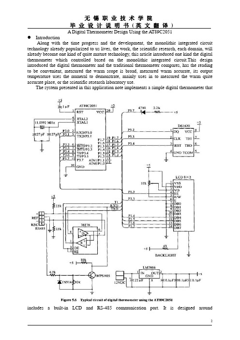
无锡职业技术学院毕业设计说明书(英文翻译)A Digital Thermometer Design Using the AT89C2051IntroductionAlong with the time progress and the development, the monolithic integrated circuit technology already popularized to us lives, the work, the scientific research, each domain, will already become one kind of quite mature technology, this article introduced one kind the digital thermometer which controlled based on the monolithic integrated circuit.This design introduced the digital thermometer and the traditional thermometer compares, has the reading to be convenient, measured the warm scope is broad, measured warm accurate, its output temperature uses the numeral to demonstrate, mainly uses in to measured the warm quite accurate place, or the scientific research laboratory use.The system presented in this application note implements a simple digital thermometer thatincludes a built-in LCD and RS-485 communication port. It is designed aroundAtmel'AT89C2051 processor, a DS1620 digital thermometer /thermostat from Dallas Semiconductor, a small 8*2 LED backlit LCD, and an RS485 line interface. The system, shown in Figure 5.6, can be used as the basis for developing custom solutions for networked and stand alone data collection and control equipment. It can be centrally powered due to its low current requirement and its small size allows it to be placed almost anywhere.●SoftwareThe LCD driver is written entirely in C and compiled under Micro-C (from Dun-field Development Systems ) using the tiny memory model. Although a canonical stack-based implementation, Micro-C includes a number of special features that make it quite suitable for generating ROMable code for small systems. The overhead incurred performing stack manipulations is made up by the library functions that are all hand coded in a highly optimized assembler. As an added benefit, Micro-C comes with fully documented library source code so special modifications can be made as circumstances arise.The first few functions contained in the LCD driver module are conventional C library implementation. PutString displays a null terminated string by merely passing characters off to PutChar until a null byte is encountered. PutChar outputs a character at a time to the LCD and handles the newline character by advancing the cursor address to the value specified by the caller. The ClearLcd function is used to clear the entire LCD and home the cursor.The functions that follow concern themselves with actual physical communication to the LCD. Since there is not a direct correspondence between the LSI’s data RAM and the LCD’s physical mapping, it is necessary to keep watch for certain boundary conditions. When a boundary is encountered, the cursor must be repositioned in order to keep the output contiguous. Since all displayable data must pass through DataWr, it makes sense to contain the corrective actions here. To handle this problem, keep track of the logical cursor positon and invoke a remedial maneuver whenever discontinuity may occur, there are two ways you can accomplish this: Read the LCD’status re gister (to get the cursor address) or Keep a local copy just for your reference.Not wanting to waste a pin to control the LCD’s read/write line (it runs in write-only mode), the latter approach was adopted.Here, the global register (IRAM actually) variable Cursor is used for this purpose. Cursor is consulted prior to any data write operation. If a correction is necessary, a new cursor address is generated and dispatched to the LCD control register via Command Wr.Following this, DateWr splits the data byte into nibbles (remember the LCD operates using a 4-bit bus) and falls through to handle the actual physical transfer. Using Micro-C’s extended preprocessor allows bit manipulation macros that expand directly to 8051 SETB and CLR instructions. Here, clear ing DRS selects the LCD’data register and DEN is toggled to generate the data strobe. Command Wr operates similarly but does not have to deal with any cursor entanglement. It selects the command register as its destination by seting DRS high prior to clocking the nibbles across the interface.The initialization function InitLcd begins at a more rudimentary nibble oriented level since no assumption can be made as to the operational status of the LCD at this time. The first three sequences ensure that the transfer mode is set to operate over a 4-bit bus. Repeating the sequence three times ensures that the command will be recognized regardless of the operational mode of the LSI. (It is wise to make no assumptions when performing any low-level initialization.) Following this, the actual operating parameters are transferred to the LCD using the standard CommandWr function. Software for this application note may be downloaded from Atmel’s Web Site or BBS.●MCUAT89C2051 MCU is a series of 51 members, It is the 8051 version of SCM. It has the following characteristics: 2 k bytes EPROM, 128 bytes RAM, 15 I / O lines, two 16 regular /counter, two five vector interrupt structure, a full two-way serial port, and includes Precision analog comparator and on-chip oscillator, a 4.25 V to 5.5 V voltage scope of work and 12 MHz/24MHz frequency, and also offers the encryption array of two program memory locking, power-down and the clock circuit.In addition, AT89C2051 also supports two kinds of software-selectable power-saving mode power supply. During my free time, CPU stop and let RAM, timing / counter, serial port and interrupt system to continue to work. Power-down can preserve the contents of RAM, but will stop oscillator chip-to prohibit all the other functions until the next hardware reset.Therefore, AT89C2051 constitute the SCM system is a simple structure, the cost of the cheapest, most efficient micro-control system, eliminating the external RAM, ROM and interface devices, reducing hardware costs, cost savings, improved The cost-effective system.MCU clock signal used to provide various micro-chip microcontroller operation of the benchmark time, the clock signal is usually used by the form of two circuits: the internal and external shocks oscillation. MCS-51 has a microcontroller internal oscillator for a reverse of the high-gain amplifier, pin XTALl and XTAL2 are here to enlarge the electrical inputs and outputs, as in-house approach, a simple circuit, from the clock Signal relatively stable, and actually used often in this way, as shown in Figure 5.6 in its external crystal oscillator (crystal) or ceramic resonator constituted an internal oscillation, on-chip high-gain amplifier and a reverse Feedback components of the chip quartz crystal or ceramic resonator together to form a self oscillator and generate oscillation clock pulse. Figure 5.6 in the external crystal and capacitors C1 and C2 constitute a parallel resonant circuits, their stability from the oscillation frequency, rapid start-up role, and its value are about 33 PF, crystal frequency of elections 12 MHz.In order to initialize the internal MCU some special function register to be reset by the way, will reset after the CPU and system components identified in the initial state, and from the initial state began work properly.MCU is reset on the circuit to achieve, in the normal operation of circumstances, as long as the RST-pin on a two machine cycle time over the high, can cause system reset, but if sustained for the RST-pin HIGH, in a circle on the MCU reset state.There are two situations in which a power-on reset and manual (switch) reduction. The system uses a power-on reset mode. Figure 5.6 in the R0 and C0 formed a power-on reset circuit, and its value for R for 8.2 K, C for the 10 uF.Digital TemperatureTemperature acquisition is handled using the DS1620 thermometer/thermostat IC from Dallas Semiconductor. The DS1620 contains all temperature measurement and signal conditioning circuitry on-chip and presents the processor with a 3-wire digital interface composed of a bi-directional data line DQ, a reset input \RST, and a clock input CLK. The temperature reading is provided in a 9-bit, two’s complement format. The measurement range spans from -55℃ to +125℃ in 0.5℃ increments. Data transfers into and out of the DS1620 are initiated by driving /RST high. Once the DS1620’s reset is released, a series of clock pulses is emitted by the processor to actually transfer the data. For transmission to the DS1620, data must be valid during the rising edge of the clock pulse. Data bits received by the processor are output on the falling edge of the clock and remain valid through the rising edge. Taking the clock high results in DQ assuming a high impedance state. The sequence can be immediately terminated by pulling \RST low which forces DQ into a high impedance state and concludes the transfer. Temperature data is transmitted over the 3-wire bus in lsb first format. A total of nine bits are transmitted where the most significant bit is the sign bit. If all nine bits are not of interest, the transfer can be terminated at any time by asserting \RST.The DS1620 support routines are coded in assembly. The DS1620 also has nonvolatile EEPROM configuration register that hold thermostatic and operational control information. TempConfig is hard-coded to set the mode for operation under CPU control and continuoustemperature conversion. Once in continuous conversion mode, the actual conversion process is started by issuing the start conversion command through TempConvert. Now the DS1620 can be read at any time and the last temperature conversion that was performed will be returned. This is accomplished by calling TempRead. The result is returned in the 16bit accumulator as defined by Micro-C consisting of the B (msb) and ACC (lsb) register.●Mainline Glue 360毕业设计网Coordination of the support drivers is managed by the main module. This module takes control after the Micro-C startup routine finishes. On entry, the code initializes the serial prot, instructs the DS1620 to start performing temperature conversions, initializes the LCD, displays a log on message, and enters into an endless loop. This loop continuously reads the DS1620, performs a Celsius to Fahrenheit conversion, translates the resulting binary number to an ASCII string, and displays the conversion result on the LCD. Periodically the code falls through and toggles an LED and transmits the temperature data serially.The Celsius to Fahrenheit conversion is performed using the familiar equation: F=C*9/5+32.Since the DS1620 returns temperature in 5℃ increments the value is first divided by 2.Unlike the often impenetrable gyrations that result when working with numbers in assembler, the C representation of this calculation is perfectly clear in intent and function. A short sequence of divisions, modules, and logical OR operations results in decimal ASCII values that make up the output string.基于AT89C2051的数字温度计的设计●导言随着时代的进步和发展,单片机技术已经普及到我们生活、工作、科研和各个领域,已经成为一种比较成熟的技术。
基于AT89C2051单片机的智能温度采集器设计

(9)负电压特性,电源极性接反时,温度计不会因发热而烧毁,但不 能正常工作。
DSl8820温度传感器的内部存储器还包括一个高速暂存RAM和一 个非易失性的可电擦除的EERAM。高速暂存RAM的结构为8个字节的
存储器。结构如图4.1所示。头丽个字节包含测得的温度信息,第三和第 四字节是TH和TL的拷贝,是易失的。每次上电复位时被刷新。第五个字 节为配置寄存器,它的内容用于确定温度值的数字转换分辨率。DSl8820 工作时按此寄存器中的分辨率将温度转换为相应精度的数值。该字节各 位的定义为,低5位一直为l,TM是测试模式位,用于设置DSl8820在工 作模式还是在测试模式。
【关键词】单片机;j[编语言;LCD液晶;DSl8820;X25045
1.引言 随着社会的发展,人们对于居住环境的舒适程度要求越来越高。采 用智能温度计可以对室内温度进行高精度采集,从而满足人们的要求。 智能温度采集器系统由单片机主控模块、测温模块、存储模块、显示 模块、键盘接口模块共5个模块组成,电路系统框图如图所示。
5.施工检验及质量控制 (1)要加强对材料的管理与检验,对每个工点按规定作好砂料的筛分 及含泥量的控制.对编制供认的得理性能及尺寸按5%的机率抽检。不合 格品严禁使用。(2)检查砂袋是否饱满。灌砂量是否满足设计值,外观有 无裂缝、鼓包现象。(3)施工检查成孔位置,深度是否达到设计要求.砂袋 入并是否顺利,露出井外长度是否与理论值相符。(4)每天检查施工记 录,并与现场井位复核,避免露打、少打。(5)对3-5%的袋装砂井进行拉
(上接第169页) 3.2.测温予程序: 测温子程序的主要功能是负责读出并处理DSl8820的测量温度值,
温度测量每le进行一次。读出温度子程序的主要功能是读出RAM中的 9个字节,在读出时需进行CRC校验,校验有错时不进行温度数据的改 写。DSl8820高速暂存器共9个存存单元。分别是:00单元,温度低字节; 01单元温度高字节;02单元用户字节l;03单元,用户字节2;04、05单元, 保留字节;06单元,计数器余值;07单元,计数器/℃;08单元。CRC。
- 1、下载文档前请自行甄别文档内容的完整性,平台不提供额外的编辑、内容补充、找答案等附加服务。
- 2、"仅部分预览"的文档,不可在线预览部分如存在完整性等问题,可反馈申请退款(可完整预览的文档不适用该条件!)。
- 3、如文档侵犯您的权益,请联系客服反馈,我们会尽快为您处理(人工客服工作时间:9:00-18:30)。
以AT89C2051单片机为控制核心的数字温度计设计
单片机控制已成为今天电子设计追-求的目标之一,本文将这种控制技术应用于温度测量中。
AT89C2051是美国Atmel公司生产的低电压、高性能CMOS8位单片机,片内含有2 KB的反复擦写的只读程序存储器和128 B的随机存取数据存储器(RAM)。
美国DALLAS半导体公司生产的DSl-8B20型单线智能温度传感器,属于新一代适配微处理器的智能传感器。
数字温度计是以DS18B20为检测元件,由AT89C2051作为主控制器的温度计,具有功耗低、结构简单、读数方便、测温范围广、测温准确的特点。
1 电路构成及工作原理
1.1 硬件设计
由AT89C2051构成的温度计主要由三部分组成:DSl8B20温度传感器、单片机AT89C2051、由LED数码管构成的显示模块。
其系统原理框图如图1所示。
DSl8B20作为单片机AT89C2051的外部信号源,把所采集到的温度转换为数字信号,通过I/O接口传给2051,2051启动ROM内的控制程序驱动LED数码管,通过I/O接口和数据线(单片机和数码管的接口)把数据传送给数码管,将采集到的温度显示出来。
1.2 总电路图。