R106中文资料
常用放大器参数
ISO106高压,隔离缓冲放大器ISO106同ISO102性能基本相同,主要区别要以下两点:①ISO106的连续隔离电压3500;②ISO106封装为40引脚DIP组件;主要引脚定义可参看ISO102。
LF147/347四JFET输入运算放大器输入失调电压1mV(LF147)、5mV(LF347);温度漂移10μV/℃;偏置电流50pA增益带宽4MHz;转换速率13V/μs;噪声20nV/(Hz^1/2)(1kHZ);消耗电流7.2mA。
±22V电源(LF147)、±18V电源(LF347);差模输入电压±38V(LF147)、±30V(LF347);共模输入电压±19V(LF147)、±15V(LF347);功耗500mW。
LF155/255/355JFET输入运算放大器输入失调电压1mV(LF155/355)、3mV(LF255);温度漂移3μV/℃(LF155/355)、5μV/℃(LF255);偏置电流30pA增益带宽GB=2.5MHz;转换速率5V/μs;噪声20nV/(Hz^1/2)(1kHZ);消耗电流2mA。
±40V电源(LF155/255)、±30V电源(LF355);共模输入电压±20V(LF155/255)、±16V(LF355);输入阻抗10^12Ω共模抑制比100dB;电压增益106dB。
LF353双JFET输入运算放大器输入失调电压5mV;温度漂移10μV/℃;偏置电流50pA;增益带宽GB=4MHz;转换速率13V/μs;噪声16nV/(Hz^1/2)(1kHZ);消耗电流1.8mA。
±18V电源;差模输入电压±30V;共模输入电压±15V;功耗500mW。
LF411/411A低失调、低漂移、JFET输入运算放大器输入失调电压800μV(LF411)、300μV(LF411A);温度漂移7μV/℃;偏置电流50pA;增益带宽GB=4MHz;转换速率15V/μs;噪声23nV/(Hz^1/2)(1kHZ);消耗电流1.8mA。
MPC106资料

Semiconductor Products SectorThis document contains information on a new product under development by Motorola.Motorola reserves the right to change or discontinue this product without notice.Technical DataMPC106 PCI Bridge/Memory Controller Hardware SpecificationsThe Motorola MPC106 PCI bridge/memory controller provides a PowerPC™ microprocessor common hardware reference platform (CHRP™) compliant bridge between the PowerPC microprocessor family and the Peripheral Component Interconnect (PCI) bus. In this document, the term ‘106’ is used as an abbreviation for the phrase ‘MPC106 PCI bridge/memory controller.’ This document contains pertinent physical characteristics of the 106. For functional characteristics, refer to the MPC106 PCI Bridge/Memory Controller User’s Manual .This document contains the following topics:TopicPageSection 1.1, “Overview”2Section 1.2, “Features”3Section 1.3, “General Parameters”5Section 1.4, “Electrical and Thermal Characteristics”5Section 1.5, “Pin Assignments”15Section 1.6, “Pinout Listings16Section 1.7, “Package Description”20Section 1.8, “System Design Information”22Section 1.9, “Document Revision History”27Section 1.10, “Ordering Information”27OverviewIn this document, the term ‘60x’ is used to denote a 32-bit microprocessor from the PowerPC architecture family that conforms to the bus interface of the PowerPC 601™, PowerPC 603™, or PowerPC 604™microprocessors. Note that this does not include the PowerPC 602™ microprocessor which has a multiplexed address/data bus. 60x processors implement the PowerPC architecture as it is specified for 32-bit addressing, which provides 32-bit effective (logical) addresses, integer data types of 8, 16, and 32 bits, and floating-point data types of 32 and 64 bits (single-precision and double-precision).To locate any published errata or updates for this document, refer to the website at /SPS/PowerPC/.1.1 OverviewThe MPC106 provides an integrated high-bandwidth, high-performance, TTL-compatible interface between a 60x processor, a secondary (L2) cache or additional (up to four total) 60x processors, the PCI bus, and main memory. This section provides a block diagram showing the major functional units of the 106 and describes briefly how those units interact.Figure 1 shows the major functional units within the 106. Note that this is a conceptual block diagram intended to show the basic features rather than how these features are physically implemented on the device.Figure 1. Block DiagramFeatures The 106 provides a PowerPC microprocessor CHRP-compliant bridge between the PowerPC microprocessor family and the PCI bus. CHRP documentation provides a set of specifications that define a unified personal computer architecture. PCI support allows the rapid design of systems using peripherals already designed for PCI and the other standard interfaces available in the personal computer hardware environment. The 106 integrates secondary cache control and a high-performance memory controller, uses an advanced, 3.3-V CMOS process technology, and is fully compatible with TTL devices.The 106 supports a programmable interface to a variety of PowerPC microprocessors operating at select bus speeds. The 60x address bus is 32 bits wide and the data bus is 64 bits wide. The 60x processor interface of the 106 uses a subset of the 60x bus protocol, supporting single-beat and burst data transfers. The address and data buses are decoupled to support pipelined transactions.The 106 provides support for the following configurations of 60x processors and L2 cache:•Up to four 60x processors with no L2 cache• A single 60x processor plus a direct-mapped, lookaside L2 cache using the internal L2 cache controller of the 106•Up to four 60x processors plus an externally controlled L2 cache (such as the Motorola MPC2605 integrated secondary cache)The memory interface controls processor and PCI interactions to main memory and is capable of supporting a variety of configurations using DRAM, EDO, SDRAM, ROM, or Flash ROM.The PCI interface of the 106 complies with the PCI Local Bus Specification, Revision 2.1, and follows the guidelines in the PCI System Design Guide, Revision 1.0,for host bridge architecture. The PCI interface connects the processor and memory buses to the PCI bus, to which I/O components are connected. The PCI bus uses a 32-bit multiplexed address/data bus, plus various control and error signals.The PCI interface of the 106 functions as both a master and target device. As a master, the 106 supports read and write operations to the PCI memory space, the PCI I/O space, and the PCI configuration space. The 106 also supports PCI special-cycle and interrupt-acknowledge commands. As a target, the 106 supports read and write operations to system memory.The 106 provides hardware support for four levels of power reduction: doze, nap, sleep, and suspend. The design of the MPC106 is fully static, allowing internal logic states to be preserved during all power-saving modes.1.2 FeaturesThis section summarizes the major features of the 106, as follows:•60x processor interface—Supports up to four 60x processors—Supports various operating frequencies and bus divider ratios—32-bit address bus, 64-bit data bus—Supports full memory coherency—Supports optional 60x local bus slave—Decoupled address and data buses for pipelining of 60x accesses—Store gathering on 60x-to-PCI writesFeatures•Secondary (L2) cache control—Configurable for write-through or write-back operation—Supports cache sizes of 256 Kbytes, 512 Kbytes, and 1 Mbyte—Up to 4 Gbytes of cacheable space—Direct-mapped—Supports byte parity—Supports partial update with external byte decode for write enables—Programmable interface timing—Supports pipelined burst, synchronous burst, or asynchronous SRAMs—Alternately supports an external L2 cache controller or integrated L2 cache module •Memory interface— 1 Gbyte of RAM space, 16 Mbytes of ROM space—Supports parity or error checking and correction (ECC)—High-bandwidth, 64-bit data bus (72 bits including parity or ECC)—Supports fast page mode DRAMs, extended data out (EDO) DRAMs, and synchronous DRAMs (SDRAMs)—Supports 1 to 8 banks of DRAM/EDO/SDRAM with sizes ranging from 2 Mbyte to 128 Mbytes per bank—ROM space may be split between the PCI bus and the 60x/memory bus (8 Mbytes each)—Supports 8-bit asynchronous ROM or 64-bit burst-mode ROM—Supports writing to Flash ROM—Configurable external buffer control logic—Programmable interface timing•PCI interface—Compliant with PCI Local Bus Specification, Revision 2.1—Supports PCI interlocked accesses to memory using LOCK signal and protocol—Supports accesses to all PCI address spaces—Selectable big- or little-endian operation—Store gathering on PCI writes to memory—Selectable memory prefetching of PCI read accesses—Only one external load presented by the MPC106 to the PCI bus—Interface operates at 20–33 MHz—Word parity supported— 3.3 V/5.0 V-compatible•Support for concurrent transactions on 60x and PCI buses•Power management—Fully-static 3.3-V CMOS design—Supports 60x nap, doze, and sleep power management modes and suspend mode •IEEE 1149.1-compliant, JTAG boundary-scan interface•304-pin ceramic ball grid array (CBGA) packageGeneral Parameters1.3 General ParametersThe following list provides a summary of the general parameters of the 106:Technology0.5 µm CMOS, four-layer metalDie size 5.8 mm x 7.2 mm (41.8 mm2)Transistor count250,000Logic design Fully-staticPackages Surface mount 304-lead C4 ceramic ball grid array (CBGA)Power supply 3.3 V ± 5% V DCMaximum input rating 5.0 V ± 10% V DC1.4 Electrical and Thermal CharacteristicsThis section provides both the AC and DC electrical specifications and thermal characteristics for the 106.1.4.1 DC Electrical CharacteristicsThe tables in this section describe the 106 DC electrical characteristics. Table 1 provides the absolute maximum ratings. Functional and tested operating conditions are given in Table 2. Absolute maximum ratings are stress ratings only, and functional operation at the maximums is not guaranteed. Stresses beyond those listed may affect device reliability or cause it permanent damage.Table 1. Absolute Maximum RatingsCharacteristic Symbol Value Unit NotesSupply voltage Vdd–0.3 to 3.6V—PLL supply voltage AVdd–0.3 to 3.6V—Input voltage V in–0.3 to 5.5V1 Junction temperature T j0 to 105°C2 Storage temperature range T stg–55 to 150°C—Notes:1Caution: V in must not exceed Vdd by more than 2.5 V at all times including during power-on reset.2The extended temperature parts have die junction temperature of -40 to 105°C. See MPC106ARXTGPNS/D for more information.Table 2 provides the recommended operating conditions for the 106. Proper device operation outside of these recommended and tested conditions is not guaranteed.Electrical and Thermal CharacteristicsTable 3 provides the package thermal characteristics for the 106.Table 4 provides the DC electrical characteristics for the 106, assuming Vdd = A Vdd = 3.3 ± 5% V DC,GND = 0 V DC, and 0 ≤ T j ≤ 105 °C.Table 5 lists the power consumption of the 106.Table 2. Recommended Operating ConditionsCharacteristic Symbol Value Unit Notes Supply voltage Vdd 3.3 ± 165 mv V —PLL supply voltage AVdd 3.3 ± 165 mv V —Input voltageV in 0 to 5.5V —Die junction temperatureT j0 to 105°CThe extended temperature parts have die junction temperature of -40 to 105°CTable 3. Package Thermal CharacteristicsCharacteristicSymbol Value Rating CBGA package thermal resistance, junction-to-top of dieθ JC0.133°C/WNote : Refer to Section 1.8, “System Design Information,” for more details about thermal management.Table 4. DC Electrical SpecificationsCharacteristicSymbol Min Max Unit Input high voltage (all inputs except SYSCLK)V IH 2 5.5V Input low voltage (all inputs except SYSCLK)V IL GND 0.8V SYSCLK input high voltage CV IH 2.4 5.5V SYSCLK input low voltage CV IL GND 0.4V Input leakage current, V in =3.3 V 1I in —15.0µA Hi-Z (off-state) leakage current, V in = 3.3 V 1 I TSI —15.0µA Output high voltage, I OH = -7 mA 2 V OH 2.4—V Output low voltage, I OL = 7 mA 2V OL —0.5V PCI 3.3 V signaling output high voltage, I OH = -0.5 mA 2 V OH 2.7—V PCI 3.3 V signaling output low voltage, I OL = 1.5 mA 2 V OL —0.3V Capacitance, V in = 0 V , f = 1 MHz 3C in—7.0pFNotes:1 Excludes test signals (LSSD_MODE and JT AG signals).2 This value represents worst case 40-ohm drivers (default value for Processor/L2 control signals CI, WT , GBL, TBST , TSIZ[0–2], TT[0–4], TWE, and TV) only. Other signals have lower default driver impedance and will support larger I OH and I OL . All drivers may optionally be programmed to different driver strengths. 3Capacitance is periodically sampled rather than 100% tested.Electrical and Thermal Characteristics1.4.2 AC Electrical CharacteristicsThis section provides AC electrical characteristics for the 106. After fabrication, parts are sorted by maximum 60x processor bus frequency, as shown in Section 1.4.2.1, “Clock AC Specifications,” and tested for conformance to the AC specifications for that frequency. These specifications are for operation between 16.67 and 33.33 MHz PCI bus (SYSCLK) frequencies. The 60x processor bus frequency is determined by the PCI bus (SYSCLK) frequency and the settings of the PLL[0–3] signals. All timings are specified relative to the rising edge of SYSCLK.1.4.2.1 Clock AC SpecificationsTable 6 provides the clock AC timing specifications as shown in Figure 2, and assumes Vdd = A Vdd = 3.3± 5% V DC, GND = 0 V DC, and 0 ≤ T j ≤ 105 °C.Table 5. Power ConsumptionModeSYSCLK/Core 33/66 MHzSYSCLK/Core 33/83.3 MHzUnitFull-OnT ypical Maximum1.22.2W 1.42.4WDozeT ypical Maximum1.0 1.1W 1.21.4WNapT ypical Maximum1.0 1.1W 1.21.4WSleepT ypical Maximum260330mW 360450mWSuspendT ypical Maximum140220mW 190270mWNotes:•Power consumption for common system configurations assuming 50 pF loads •Suspend power-saving mode assumes SYSCLK off and PLL in bypass mode.•T ypical power is an average value measured at Vdd = AVdd = 3.30 V and T A = 25 °C. •Maximum power is measured at Vdd = AVdd = 3.45 V and T A= 25 °C.Electrical and Thermal CharacteristicsFigure 2 provides the SYSCLK input timing diagram.Figure 2. SYSCLK Input Timing Diagram1.4.2.2 Input AC SpecificationsTable 7 provides the input AC timing specifications for the 106 as defined in Figure 3 and Figure 4. These specifications are for operation between 16.67 and 33.33 MHz PCI bus clock (SYSCLK) frequencies.Assume Vdd = A Vdd = 3.3 ± 5% V DC, GND = 0 V DC, and 0 ≤ T j ≤ 105 °C.Table 6. Clock AC Timing SpecificationsNum Characteristic SYSCLK/Core 33/66 MHz SYSCLK/Core 33/83.3 MHz Unit NotesMinMax Min Max —60x processor bus (core) frequency 16.676616.6783.3MHz 1—VCO frequency 120200120200MHz 1, 2—SYSCLK frequency 16.6733.3316.6733.33MHz 11SYSCLK cycle time 30.060.030.060.0ns —2, 3SYSCLK rise and fall time— 2.0— 2.0ns 34SYSCLK duty cycle measured at 1.4 V 40604060%4—SYSCLK jitter—±200—±200ps 5—106 internal PLL relock time—100—100µ s4, 6Notes :1 Caution : The SYSCLK frequency and PLL[0–3] settings must be chosen such that the resulting SYSCLK (bus) frequency, CPU (core) frequency, and PLL (VCO) frequency do not exceed their respective maximum or minimum operating frequencies. Refer to the PLL[0–3] signal description in Section 1.8, “System Design Information,” for valid PLL[0–3] settings, and to Section 1.9, “Document Revision History,” for available frequencies and part numbers.2 VCO operating range for extended temperature devices is different. Refer to MPC106ARXTGPNS/D for more information.3 Rise and fall times for the SYSCLK input are measured from 0.4 V to 2.4 V . 4 Timing is guaranteed by design and characterization and is not tested.5 The total input jitter (short-term and long-term combined) must be under ±200 ps.6PLL-relock time is the maximum time required for PLL lock after a stable Vdd, AVdd, and SYSCLK are reached during the power-on reset sequence. This specification also applies when the PLL has been disabled andsubsequently re-enabled during the sleep and suspend power-saving modes. Also note that HRST must be held asserted for a minimum of 255 bus clocks after the PLL-relock time (100 µs) during the power-on reset sequence.Electrical and Thermal CharacteristicsFigure 3 provides the input timing diagram for the 106.Table 7. Input AC Timing SpecificationsNumCharacteristic66 MHz83.3 MHzUnitNotesMinMaxMin Max10a Group I input signals valid to 60x Bus Clock (input setup) 4.0 3.5ns 1,2,310a Group II input signals valid to 60x Bus Clock (input setup) 3.5 3.5ns 1,2,410a Group III input signals valid to 60x Bus Clock (input setup) 3.0 2.5ns 1,2,510a Group IV input signals valid to 60x Bus Clock (input setup) 5.0 4.0ns 1,2,610b Group V input signals valid to SYSCLK (input setup)7.07.0ns 7,810b Group VI input signals valid to SYSCLK (input setup)7.07.0ns 7,911a 60x Bus Clock to group I–IV inputs invalid (input hold)0—0—ns 3,4,5,611b SYSCLK to group V–VI inputs invalid (input hold)–0.5—–0.5—ns8,9HRST pulse width255 x t sysclk + 100 µs —255 x t sysclk + 100 µs ——10c Mode select inputs valid to HRST (input setup) 3 x t sysclk— 3 x t sysclk—ns 10, 11,1211c HRST to mode select input invalid (input hold)1.0—1.0—ns10, 12Notes:1Input specifications are measured from the TTL level (0.8 or 2.0 V) of the signal in question to the 1.4 V of the rising edge of SYSCLK. Both input and output timings are measured at the pin (see Figure 3).2Processor and memory interface signals are specified from the rising edge of the 60x bus clock (which is internally synchronized to SYSCLK).3Group I input signals include the following processor, L2, and memory interface signals: A[0–31], P AR[0–7]/AR[1–8], BR[0–4], BRL2, XA TS, LBCLAIM, ADS, BA0, TV and HIT (when configured for external L2)4Group II input signals include the following processor and memory interface signals: TBST , TT[0–4], TSIZ[0–2], WT , CI, GBL, AACK, and T A.5Group III input signals include the following processor and memory interface signals: DL[0–31] and DH[0–31].6Group IV input signals include the following processor and L2 interface signals: TS, ARTRY , DIRTY_IN, and HIT (when configured for internal L2 controller).7PCI 3.3 V signaling environment signals are measured from 1.65 V (Vdd ÷ 2) on the rising edge of SYSCLK to V OH = 3.0 V or V OL = 0.3 V . PCI 5 V signaling environment signals are measured from 1.65 V (Vdd ÷ 2) on the rising edge of SYSCLK to V OH = 2.4 V or V OL = 0.55 V .8Group V input signals include the following bussed PCI interface signals: FRAME, C/BE[0–3], AD[0–31], DEVSEL, IRDY , TRDY , STOP , P AR, PERR, SERR, LOCK, FLSHREQ, and ISA_MASTER.9Group VI input signal is the point-to-point PCI GNT input signal.10The setup and hold time is with respect to the rising edge of HRST (see Figure 4). Mode select inputs include the RCS0, FOE, and DBG0 configuration inputs.11 tsysclk is the period of the external clock (SYSCLK) in nanoseconds (ns). When the unit is given as t sysclk , the numbers given in the table must be multiplied by the period of SYSCLK to compute the actual time duration (in nanoseconds) of the parameter in question.12These values are guaranteed by design and are not tested.Electrical and Thermal CharacteristicsFigure 3. Input Timing DiagramFigure 4 provides the mode select input timing diagram for the 106.Figure 4. Mode Select Input Timing Diagram1.4.2.3 Output AC SpecificationsTable 8 provides the output AC timing specifications for 106 (shown in Table 5). Assume Vdd = A Vdd =3.3 ± 5% V DC, GND = 0 V DC, CL = 50 pF, and 0 ≤ T j ≤ 105 °C. Processor and memory interface signals are specified from the rising edge of the 60x bus clock (which is internally synchronized to SYSCLK). All units are nanoseconds.VM = Midpoint Voltage (1.4 V)HRSTMODE PINSElectrical and Thermal Characteristics Table 8. Output AC Timing SpecificationsNum Characteristic66 MHz83.3 MHzNotes Min Max Min Max12SYSCLK to output driven (outputenable time)2.0— 2.0—113a SYSCLK to output valid for TS andARTRY—7.0— 6.02, 3, 413b SYSCLK to output valid for all non-PCIsignals except TS, ARTRY, RAS[0–7],CAS[0–7], and DWE[0-2]—7.0— 6.02, 3, 514a SYSCLK to output valid (for RAS[0–7]and CAS[0–7])—7.0— 6.02, 3 14b SYSCLK to output valid for PCI signals—11.0—11.03, 615a SYSCLK to output invalid for allnon-PCI signals (output hold)1.0— 1.0—7, 1015b SYSCLK to output invalid for PCIsignals (output hold)1.0— 1.0—718SYSCLK to ARTRY high impedancebefore precharge (output hold)—8.0—8.0119SYSCLK to ARTRY precharge enable (0.4 *t sysclk) + 2.0—(0.4 xt sysclk) + 2.0—8, 121SYSCLK to ARTRY high impedance after precharge —(1.5 *t sysclk) + 8.0—(1.5 xt sysclk) + 8.08, 1Notes:1These values are guaranteed by design and are not tested.2Output specifications are measured from 1.4 V on the rising edge of the appropriate clock to the TTL level (0.8 V or 2.0 V) of the signal in question. Both input and output timings are measured at the pin (see Figure 5).3The maximum timing specification assumes C L = 50 pF.4The shared outputs TS and ARTRY require pull-up resistors to hold them negated when there is no bus master driving them.5When the 106 is configured for asynchronous L2 cache SRAMs, the DWE[0–2] signals have a maximum SYSCLK to output valid time of (0.5 x t PROC) + 8.0 ns (where t PROC is the 60x bus clock cycle time).6PCI 3.3 V signaling environment signals are measured from 1.65 V (Vdd ÷ 2) on the rising edge of SYSCLK to V OH = 3.0 V or V OL = 0.3 V.7The minimum timing specification assumes C L = 0 pF.8tsysclk is the period of the external bus clock (SYSCLK) in nanoseconds (ns). When the unit is given as t sysclk the numbers given in the table must be multiplied by the period of SYSCLK to compute the actual time duration (in nanoseconds) of the parameter in question.9PCI devices which require more than the PCI-specified hold time of Th = 0ns or systems where clock skewapproaches the PCI-specified allowance of 2ns may not work with the MPC106. For workarounds, see Motorola application note Designing PCI 2.1-Compliant MPC106 Systems (order number AN1727/D).Electrical and Thermal CharacteristicsFigure 5 provides the output timing diagram for the 106.Figure 5. Output Timing Diagram1.4.3 JTAG AC Timing SpecificationsTable 9 provides the JTAG AC timing specifications. Assume Vdd = A Vdd = 3.3 ± 5% V DC, GND = 0 V DC, CL = 50 pF, and 0 ≤ T j ≤ 105 °C.Table 9. JTAG AC Timing Specifications (Independent of SYSCLK)Num CharacteristicMin Max Unit Notes —TCK frequency of operation 025MHz —1TCK cycle time40—ns —2TCK clock pulse width measured at 1.4 V 20—ns —3TCK rise and fall times03ns 14TRST setup time to TCK rising edge 10—ns 25TRST assert time10—ns160x Bus ClockALL Non-PCI TSARTRYVM = Midpoint Voltage (1.4V)(Except TS andARTRY)SYSCLKALLOUTPUTS PCI OUTPUTSElectrical and Thermal CharacteristicsFigure 6 provides the JTAG clock input timing diagram.Figure 6. JTAG Clock Input Timing DiagramFigure 7 provides the TRST timing diagram.Figure 7. TRST Timing Diagram6Boundary-scan input data setup time 5—ns 37Boundary-scan input data hold time 15—ns 38TCK to output data valid 030ns 49TCK to output high impedance 030ns 410TMS, TDI data setup time 5—ns —11TMS, TDI data hold time 15—ns 112TCK to TDO data valid 015ns —13TCK to TDO high impedance15ns—Notes :1These values are guaranteed by design, and are not tested2TRST is an asynchronous signal. The setup time is for test purposes only.3Non-test signal input timing with respect to TCK.4Non-test signal output timing with respect to TCK.Table 9. JTAG AC Timing Specifications (Independent of SYSCLK) (Continued)Num CharacteristicMin Max Unit NotesTCKVM = Midpoint Voltage (1.4 V)TRSTTCKElectrical and Thermal CharacteristicsFigure 8 provides the boundary-scan timing diagram.Figure 9. Test Access Port Timing DiagramTCKData InputsData OutputsData OutputsData OutputsTCKTDI, TMSTDOTDOTDOPin Assignments1.5 Pin AssignmentsFigure 10 contains the pin assignments for the MPC106, and Figure 11 provides a key to the shading.Figure 11. Pin Assignments Shading Key16151413121110987654321WW V V U U TT R R P P N N M M L L K K J J H H G G F F E E D D C C B B AA16151413121110987654321Figure 10. Pin AssignmentsNo ConnectPower Supply GroundPower Supply PositiveAVddClock Power Supply Positive (K9)VIEWSignalsPinout Listings1.6 Pinout ListingsTable 10 provides the pinout listing for the MPC106. S ome signals have dual functions and are shown more than once.Table 10. Pinout ListingSignal Name Pin Number Active I/O60x Processor Interface SignalsHigh I/O A[0–31]R2, P2, N2, M2, L2, K2, J5, K4, K5, K6, J2, J6, J3, J4, H3,H4, H2, G2, F1, E1, E2, F4, E3, D1, C1, C2, B1, C3, B2, E4,D3, E5AACK D2Low I/OARTRY F2Low I/OBG0K3Low OutputBG1R4Low Output (DIRTY_OUT)R5Low Output BG2(TWE)T1Low Output BG3(DCS)BR0L3Low InputT3Low Input BR1(DIRTY_IN)T6Low Input BR2(TV)T5Low Input BR3(BA0)CI N3Low I/ODBG0L5Low OutputU4Low Output DBG1(TOE)DBG2P3Low Output (DWE0)H11Low Output DBG3(DWE1)DBGLBJ10Low Output (CKE)DH[0–31]T14, R13, R14, P13, P14, N13, U3, W1, V2, W2, V3, W3, V4,High I/OW4, V5, W5, V6, W6, V7, W7, V8, W8, N8, W9, V9, W10, V10,W11, V11, W12, V12, W13High I/O DL[0–31]U6, T7, U7, T8, U8, R8, P8, N9, P9, R9, U9, T9, U10, T10,U13, T13, R12, N14, M13, T2, U1, U2, V1, U15, V16, U14,W16, V15, W15, V14, W14, V13GBL M3Low I/OPinout ListingsLBCLAIM N4Low InputMCP J11Low OutputT A N1Low I/OTBST L4Low I/OTEA J1Low OutputTS R1Low I/O TSIZ[0–2]G3, G4, F3High I/OTT[0–4]G1, H1, K1, L1, M1High I/OWT M4Low I/OXA TS(SDMA1)P1Low InputL2 Cache Interface SignalsADS/DALE/BRL2R3Low I/O BA0(BR3)T5Low Output BA1/BAA/BGL2P4Low Output DBGL2/DOE U5Low Output DCS(BG3)T1Low OutputDIRTY_IN(BR1)T3Low InputDIRTY_OUT(BG1)R4Low OutputDWE0(DBG2)P3Low OutputDWE1(DBG3)H11Low OutputDWE2(CKO)L11Low Output HIT T4Low InputTOE(DBG1)U4Low OutputTV(BR2)T6High I/OTWE(BG2)R5Low Output Memory Interface SignalsBCTL[0–1]F16, F15Low OutputBERR (ISA_MASTER)B3Low Input Table 10. Pinout Listing (Continued)Signal Name Pin Number Active I/OPinout ListingsCAS/DQM[0–7]J15, H15, G16, E16, G14, G13, F14, E14Low Output CKE/DBGLBJ10High Output FOED13Low Output MA0/SDBA1/SDMA0/AR0N15High Output SDMA1(XA TS)P1High Output MA1/SDBA0/AR9U16High Output MA[2–12]/SDMA[2–12]/AR [10–20]T16, R16, P15, P16, N16, M15, M16, L15, K15, K16, J16High Output MDLE/SDCAS E13Low Output P AR[0–7]/AR[1–8]D16, D15, C16, C15, B16, C14, A16, B15High I/O PPEN J14Low Output RAS/CS[0–7]M14, L13, K13, K14, K12, L10, J12, K11Low Output RCS0R15Low I/O RCS1J13Low Output RTC G15High Input SDRAS (PIRQ)H10Low Output WET15LowOutputPCI Interface Signals1AD[31–0]A4, C13, B5, D12, A5, C12, B6, D11, C11, B7, D10, A7, C10, B8, D9, A8, B10, D8, A11, C7, B11, D7, A12, C6, B12, C5, A13, D5, A14, C4, B14, D4High I/OC/BE[3–0]A6, C9, C8, D6Low I/O DEVSEL F8Low I/O FLSHREQ A3Low Input FRAME A10Low I/O GNT A15Low Input IRDY E8Low I/O ISA_MASTER (BERR)B3Low Input LOCK G8Low Input MEMACK A2Low Output P AR G9High I/O PERR F9Low I/O PIRQ (SDRAS)H10Low Output REQB4LowOutputTable 10. Pinout Listing (Continued)Signal Name Pin NumberActive I/OPinout ListingsSERR E9Low I/O STOP A9Low I/O TRDYB9LowI/OInterrupt, Clock, and Power Management SignalsCKO (DWE2)L11High Output HRST L16Low Input NMI E15High Input QACK L14Low Output QREQ H16Low Input SYSCLK L6Clock Input SUSPENDH14LowInputTest/Configuration SignalsPLL[0–3]U11, T11, U12, T12High Input TCK F13Clock Input TDI B13High Input TDO E12High Output TMS D14High Input TRSTH13LowInputPower and Ground SignalsAVdd K9High Clock Power LSSD_MODE 2G11Low Input Vdd E10, E6, F11, F5, F7, G10, G12, G6, H5, H7, K10, K7, L12, M11, M5, M7, N10, N12, N6, P11, P5, P7, R10, R6, J8, L8High Power Vss E11, E7, F10, F12, F6, G5, G7, H12, H6, J7, L7, M10, M12, M6, N11, N5, N7, P10, P12, P6, R11, R7, K8, J9, L9Low Ground NCH8, H9, M8, M9——Note:1All PCI signals are in little-endian bit order.2This test signal is for factory use only. It must be pulled up to Vdd for normal device operation.Table 10. Pinout Listing (Continued)Signal NamePin NumberActive I/O。
kohl's defect list 中文翻译

主要疵点分类表——家纺主要疵点1..疵点影响了产品的外观,使用和质量以至于:客人看到疵点不会购买商品初次使用后因质量问题引起不满疵点造成的拒付通常要求供货商在装运之前仔细的检查和重新审计。
2. 产品必须达到一定的性能标准或测试要求1主要疵点=1分布料和颜色F01洞孔——纱线的断点(包括两头或经纬纱上的极小断点)漏针——编织上的缝纫故障会造成脱针断头——经纱断裂后并经过修补的地方,特别是可以看见织到织物当中的明显断头。
F02条花疵——由弯针造成的垂直裂缝硬折痕疵——由于在缩水率控制和稳定过程中采用起皱织物而造成的坚硬折痕。
横裆疵——物横列或在织物横向上通常会出现一些不均匀的花纹图案。
原因是纱线不均匀、纱线张力不均匀以及纱线具有不同的染料亲和力。
粗经疵——有一根经纱的直径要明显大于织物正常经纱的直径。
起毛不匀在一组套件中出现不同绒面,例如毛巾F03 切断纱向——不按经纱、条纹方向剪裁影响美观,造成缩水。
F04 影响美观的结、斑块或纱头F05彩色飞花织入疵,影响产品美观F06缺纬——编织纹由于缺纬而破坏F07影响美观的泥点、油斑、污点F08 织布水洗洗、织物整理不均,例如:存在过渡磨损、明显的水洗差异,或者与要求不符。
F09 乳胶衬里破损,能明显看到喷射在毯子前的乳胶衬里F10 影响美观的不均匀印染或色斑F11 违背已经认可的员工、加工标准F12 扭曲、压弯或严重起皱零件&装饰T01 未经允许的零件装饰影响了产品性能,例如:不正确的内衬、劣等松紧带、相对于经线包边的斜纹包边T02 指定的零件装饰没有按照指定要求意外的丢失、破损、瑕疵、损耗线向不正,影响产品外观和品质型号、尺寸、颜色、位置与要求不符不符合要求的不配套的色线或配件内衬/衬料内衬必须与布料合适;例如不合适的易熔化配件如果有衬里,在完成包边后,衬里不可露出。
在产品表面不可出见衬里、衬头掉线粘衬不可穿透纽扣:丢失;破损、瑕疵、定反的纽扣;与要求(例,式样)不符的纽扣;配件爱你与要求不符;纽扣小于14莱茵必须有4个孔拉链:失灵;不可使用爪型定位停止梢;使用铝制拉链;拉链部件未按指定要求,影响产品品质美观(例如,拉链齿、拉链牌、拉链带、拉链颜色、尺寸、长度);拉链带边缘露出,易扎手;所有拉链滑动必须是锁式的,也可是自动锁、半自动锁、针锁式。
H3C_S5130EI_E-CMW710-R3116_版本说明书

3 软件特性及命令行变更说明 ······························································································ 10 4 MIB变更说明 ················································································································· 10 5 操作方式变更说明··········································································································· 12
1.1 版本号 ························································································································1 1.2 历史版本信息···········································································ቤተ መጻሕፍቲ ባይዱ····································1 1.3 版本配套表···················································································································5 1.4 版本升级注意事项··········································································································7
ISO106中文资料
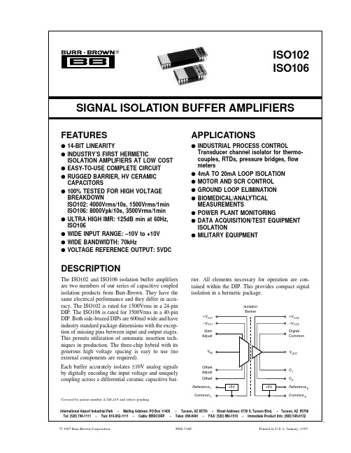
SIGNAL ISOLATION BUFFER AMPLIFIERSAPPLICATIONSq INDUSTRIAL PROCESS CONTROLTransducer channel isolator for thermo-couples, RTDs, pressure bridges, flowISOLATION AMPLIFIERS AT LOW COST2®ISO102/106SPECIFICATIONSELECTRICALAt T A = +25°C and V CC1 = V CC2 = ±15V unless otherwise noted.ISO102, ISO106, ISO102B, ISO106BPARAMETERCONDITIONSMINTYPMAXUNITSISOLATION VoltageRated Continuous (1)ISO102:AC, 60HzT MIN to T MAX 1500Vrms DCT MIN to T MAX 2121VDC ISO106:AC, 60HzT MIN to T MAX 3500Vrms DCT MIN to T MAX4950VDC Test Breakdown, AC, 60Hz ISO10210s 4000Vrms ISO10610s8000Vpk Isolation-Mode Rejection (2)V ISO = Rated Continuous, 60HzAC:ISO102115120dB 12µVrms/V ISO106125130dB 0.30.6µVrms/V DC140160dB 0.010.10µVDC/V Barrier Resistance 1014ΩBarrier Capacitance 6pF Leakage Current V ISO = 240Vrms, 60Hz 0.51µArms INPUTVoltage Range Rated Operation–10+10V Resistance 75100k ΩCapacitance 5pF OUTPUTVoltage RangeRated Operation –10+10V Derated Operation–12+12V Current Drive±5mA Short Circuit Current 92050mA Ripple Voltage (6) f = 0.5MHz to 1.5MHz3mVp-p Resistance0.31ΩCapacitive Load Drive Capability 10,000pF Overload Recovery Time, 0.1%|V O | > 12V30µs OUTPUT VOLTAGE NOISE Voltage:f = 0.1Hz to 10Hz300µVp-p f = 0.1Hz to 70kHz16µV/ Hz Dynamic Range (7):f = 0.1Hz to 70kHz12-Bit Resolution, 1LSB, 20V FS 74dB f = 0.1Hz to 280Hz 16-Bit Resolution, 1LSB, 20V FS96dB FREQUENCY RESPONSE Small Signal Bandwidth70kHz Full Power Bandwidth, 0.1% THD V O = ±10V 5kHz Slew RateV O = ±10V 0.5V/µs Settling Time, 0.1%V O = –10V to +10V100µs Overshoot, Small Signal (8)C 1 = C 2 = 040%VOLTAGE REFERENCES Voltage Output, Ref 1, Ref 2No Load +4.975+5+5.025VDC B GradeNo Load+4.995+5+5.005VDC vs Temperature ±520ppm/°C vs Supplies 10µV/V vs Load4001000µV/mA Current Output–0.1+5mA Short Circuit Current 61430mA POWER SUPPLIESRated Voltage, ±V CC1, ±V CC2Rated Performance±15V Voltage Range±10±20V Quiescent Current:+V CC1No Load+11+15mA –V CC1–9–12mA +V CC2+25+33mA –V CC2–15–20mA Dissipation:±V CC1300400mW ±V CC2600800mW TEMPERATURE RANGE Specification –25+85°C Operating (9)–25+85°C Storage–65+150°C Thermal Resistance, θJA40°C/W θJC12°C/W3®ISO102/106ELECTRICAL (CONT)ISO102ISO102B PARAMETER CONDITIONSMINTYP MAXMINTYP MAXUNITS GAINNominal Gain 1*V/V Initial Error (3)±0.1±0.250.070.13% FSR Gain vs Temperature ±20±50±12±25ppm FSR/°C Nonlinearity (4)V O = –10V to +10V±0.007±0.012±0.002±0.003% FSRINPUT OFFSET VOLTAGE Initial OffsetV IN = 0V±25±70±15±25mV vs Temperature ±250±500±150±250µV/°C vs Power Supplies (5)Input Stage, V CC1 = ±10V to ±20V 0 1.4 4.0***mV/V Output Stage, V CC2 = ±10V to ±20V–4–1.4***mV/VThe information provided herein is believed to be reliable; however, BURR-BROWN assumes no responsibility for inaccuracies or omissions. BURR-BROWN assumes no responsibility for the use of this information, and all use of such information shall be entirely at the user’s own risk. Prices and specifications are subject to change without notice. No patent rights or licenses to any of the circuits described herein are implied or granted to any third party. BURR-BROWN does not authorize or warrant any BURR-BROWN product for use in life support devices and/or systems.ISO106ISO106B PARAMETER CONDITIONSMINTYP MAXMINTYP MAXUNITS GAINNominal Gain 1*V/V Initial Error (3)±0.1±0.250.07*% FSR Gain vs Temperature ±20±50±12±25ppm FSR/°C Nonlinearity (4)V O = –10V to +10V±0.04±0.075±0.007±0.025% FSRINPUT OFFSET VOLTAGE Initial OffsetV IN = 0V±25±70**mV vs Temperature ±250±500±150±250µV/°C vs Power Supplies (5)Input Stage, V CC1 = ±10V to ±20V 3.7*mV/V Output Stage, V CC2 = ±10V to ±20V–3.7*mV/V* Specification same as model to the left.NOTES: (1) 100% tested at rated continuous for one minute. (2) Isolation-mode rejection is the ratio of the change in output voltage to a change in isolation barrier voltage.It is a function of frequency as shown in the Typical Performance Curves. This is specified for barrier voltage slew rates not exceeding 100V/µs. (3) Adjustable to zero.FSR = Full Scale Range = 20V. (4) Nonlinearity is the peak deviation of the output voltage from the best fit straight line. It is expressed as the ratio of deviation to FSR.(5) Power supply rejection = change in V OS /20V supply change. (6) Ripple is the residual component of the barrier carrier frequency generated internally. (7) Dynamic range = FSR/(voltage spectral noise density x square root of user bandwidth). (8) Overshoot can be eliminated by band-limiting. (9) See “Power Dissipation vs Temperature” performance curve for limitations. (10) Band limited to 10Hz, bypass capacitors located less than 0.25" from supply pins.NOTE: (1) For detailed drawing and dimension table, please see end of data sheet, or Appendix D of Burr-Brown IC Data Book.4®ISO102/106PIN CONFIGURATION–V V Gain Adjust Common C Common Reference +V +V Offset Adjust Offset Reference Digital Common C V –V 1 2 3 4 9 10 11 1224 23 22 21 16 15 14 13CC1CC2CC1ISO1021OUT CC22 IsolationBarrierIN112 2–V V Gain Adjust Common C Common Reference +V +V Offset Adjust Offset Reference Digital Common C V –V 1 2 3 4 17 18 19 2040 39 38 37 24 23 22 21CC1CC2 CC1ISO1061OUT CC22 IsolationBarrierIN112 2PIN DESCRIPTIONS±V CC1,Positive and negative power supply voltages and common (or ground) for the input stage. Common 1 is the analog reference voltage for input Common 1signals. The voltage between Common 1 and Common 2 is the isolation voltage and appears across the internal high voltage barrier.±V CC2,Positive and negative power supply voltages and common (or ground) for the output stage. Common 2 is the analog reference voltage for output Common 2signals. The voltage between Common 1 and Common 2 is the isolation voltage and appears across the internal high voltage barrier.V IN Signal input pin. Input impedance is typically 100k Ω. The input range is rated for ±10V. The input level can actually exceed the input stage supplies. Output signal swing is limited only by the output supply voltages.Gain This pin is an optional signal input. A series 5k Ω potentiometer between this pin and the input signal allows a guaranteed ±1.5% gain adjustment Adjust range. When gain adjustment is not required, the Gain Adjust should be left open. Figure 4 illustrates the gain adjustment connection.Reference 1+5V reference output. This low-drift zener voltage reference is necessary for setting the bipolar offset point of the input stage. This pin must be strapped to either Offset or Offset Adjust to allow the isolation amplifier to function. The reference is often useful for input signal conditioning circuits. See “Effect of Reference Loading on Offset” performance curve for the effect of offset voltage change with reference loading.Reference 1 is identical to, but independent of, Reference 2. This output is short circuit protected.Reference 2+5V reference output. This reference circuit is identical to, but independent of, Reference 1. It controls the bipolar offset of the output stage through an internal connection. This output is short-circuit protected.Offset Offset input. This input must be strapped to Reference 1 unless user adjustment of bipolar offset is required.Offset This pin is for optional offset control. When connected to the Reference 1 pin through a 1k Ω potentiometer, ±150mV of adjustment range is Adjust guaranteed. Under this condition, the Offset pin should be connected to the Offset Adjust pin. When offset adjustment is not required, the Offset Adjust pin is left open. See Figure 4.Digital Digital common or ground. This separate ground carries currents from the digital portions of the output stage circuit. The best grounding practi-Common ces require that digital common current does not flow in analog common connections. Both pins can be tied directly to a ground plane if available.Difference in potentials between the Common 2 and Digital Common pins can be ±1V. See Figure 2.V OUTSignal output. Because the isolation amplifier has unity gain, the output signal is ideally identical to the input signal. The output is low impedance and is short-circuit protected. This signal is referenced to Common 2; subsequent circuitry should have a separate “sense” connection to Common 1as well as V OUT .C 1, C 2Capacitors for small signal bandwidth control. These pins connect to the internal rolloff frequency controlling nodes of the output low-pass filter.Additional capacitance added to these pins will modify the bandwidth of the buffer. C 2 is always twice the value of C 1. See “Bandwidth Control”performance curve for the relationship between bandwidth and C 1 and C 2. When no connections are made to these pins, the full small-signal bandwidth is maintained. Be sure to shield C 1 and C 2 pins from high electric fields on the PC board. This preserves AC isolation-mode rejection by reducing capacitive coupling effects.5®ISO102/106TYPICAL PERFORMANCE CURVEST A = +25°C, V CC = ±15VDC unless otherwise noted.ISOLATION-MODE REJECTION vs ISOLATION VOLTAGE FREQUENCYIsolation Voltage Frequency (Hz)I s o l a t i o n -M o d e R e j e c t i o n (d B )1601401201008060 101M1001k10k100kDYNAMIC RANGE vs BANDWIDTHSmall Signal Bandwidth (Hz)Bandwidth Control Capacitors (F)D y n a m i c R a n g e (d B )120110100908070 110 100 1k 10k 100k 3µ300n30n3nF300p30pBW — C — 1ISOLATION LEAKAGE CURRENT vs ISOLATION VOLTAGE FREQUENCYIsolation Voltage Frequency (Hz)I s o l a t i o n L e a k a g e C u r r e n t (A )101M10m1m100µ10µ1µ100n1001k10k100kIsolation Voltage (V)Rated10.5–0.5–1210 –1 –2 GainOffsetT = T to T MIN MAX∆ GAIN ERROR AND ∆ OFFSET VOLTAGEvs ISOLATION VOLTAGEG a i n E r r o r (%)∆ ∆ O f f s e t V o l t a g e (m V )BANDWIDTH CONTROLC 1 (F)S m a l l S i g n a l B a n d w i d t h (H z )1M100k10k 1k 10010 13p30p300p3n 30n300n 3µPOWER DISSIPATION vs TEMPERATUREAmbient Temperature (°C)M a x i m u m P o w e r D i s s i p a t i o n (W )1.61.41.210.80M a x i m u m P o w e r S u p p l i e s (V )±20±15±106®ISO102/106TYPICAL PERFORMANCE CURVES (CONT)T A = +25°C, V CC = ±15VDC unless otherwise noted.LARGE SIGNAL TRANSIENT RESPONSETime (µs)100200 30040015 105 0 –5 –10 –15O u t p u t V o l t a g e (V )TOTAL HARMONIC DISTORTIONFrequency (Hz)1001k 10k100kT H D + N o i s e (%)1010.10 RECOMMENDED RANGE OF ISOLATION VOLTAGEIsolation Voltage Frequency (Hz)1k10k100k1M10k M a x i m u m I s o l a t i o n V o l t a g e (V p k )1k10010 2k 5kGAIN/PHASE vs FREQUENCY101001k10k100kFrequency (Hz)S m a l l S i g n a l G a i n (d B )6–6–12–1890–90–180–270P h a s e S h i f t (d e g r e e s )OUTPUT SPECTRAL NOISE DENSITY40 35 30 25 20 15 10 5 0 S p e c t r a l N o i s e D e n s i t y (d B H z )10µV / H z 01020 30 40 50 Frequency (kHz) N: 128 : 125Hz FS: –47dBVβ GAIN FLATNESS vs FREQUENCY0 1 2 3 4 5 6 7 8Frequency (kHz)L a r g e S i g n a l G a i n (d B )0.030.02 0.01 0 –0.01 –0.02 –0.037®ISO102/106TYPICAL PERFORMANCE CURVES (CONT)T A = +25°C, V CC = ±15VDC unless otherwise noted.FIGURE 1. Simplified Diagram of ISO102 and ISO106.THEORY OF OPERATIONThe ISO102 and ISO106 have no galvanic connection be-tween the input and output. The analog input signal refer-enced to the input common is accurately duplicated at the output referenced to the output common. Because the barrier information is digital, potentials between the two commons can assume a wide range of voltages and frequencies with-out influencing the output signal. Signal information re-mains undisturbed until the slew rate of the barrier voltage exceeds 100V/µs. The isolation amplifier’s ability to reject fast dV/dt changes between the two grounds is specified as transient immunity. The amplifier is protected from damage for slew rates up to 100,000V/µs.A simplified diagram of the ISO102 and ISO106 is shown in Figure 1. The design consists of an input voltage-controlled oscillator (VCO) also known as a voltage-to-frequency con-verter (VFC), differential capacitors, and output phase lock loop (PLL). The input VCO drives digital levels directly into the two 3pF barrier capacitors. The digital signal is fre-quency modulated and appears differentially across the bar-rier, while the externally applied isolation voltage appears common-mode.EFFECT OF REFERENCE LOADING ON OFFSETVoltage Reference Load (mA)1250–50O u t p u t O f f s e t (m V )0.010.005–0.005–0.01ISO102B TYPICAL LINEARITY–100 10V OUT = V IN (V)N o n l i n e a r i t y (%)5–58®ISO102/106A sense amplifier detects only the differential information.The output stage decodes the frequency modulated signal by the means of a PLL. The feedback of the PLL employs a second VCO that is identical to the encoder VCO. The PLL forces the second VCO to operate at the same frequency (and phase) as the encoder VCO; therefore, the two VCOs have the same input voltage. The input voltage of the decoder VCO serves as the isolation buffer’s output signal after passing through a 100kHz second-order active filter.For a more detailed description of the internal operation of the ISO102 and ISO106, refer to Proceedings of the 1987International Symposium on Microelectronics, pages 202-206.ABOUT THE BARRIERFor any isolation product, barrier composition is of para-mount importance in achieving high reliability. Both the ISO102 and ISO106 utilize two 3pF high voltage ceramic coupling capacitors. They are constructed of tungsten thick film deposited in a spiral pattern on a ceramic substrate.Capacitor plates are buried in the package, making the barrier very rugged and hermetically sealed. Capacitance results from the fringing electric fields of adjacent metal runs. Dielectric strength exceeds 10kV and resistance is typically 1014Ω. Input and output circuitry are contained in separate solder-sealed cavities, resulting in the industry’s first fully hermetic hybrid isolation amplifier.FIGURE 3. Technique for Wiring Analog and Digital Com-mons Together.FIGURE 2. Power Supply and Signal Connection.The ISO102 and ISO106 are designed to be free from partial discharge at rated voltages. Partial discharge is a form of localized breakdown that degrades the barrier over time.Since it does not bridge the space across the barrier, it is difficult to detect. Both isolation amplifiers have been exten-sively evaluated at high temperature and high voltage.POWER SUPPLY AND SIGNAL CONNECTIONS Figure 2 shows the proper power supply and signal connec-tions. Each supply should be AC-bypassed to Analog Com-mon with 0.1µF ceramic capacitors as close to the amplifier as possible. Short leads will minimize lead inductance. A ground plane will also reduce noise problems. Signal com-mon lines should tie directly to the common pin even if a low impedance ground plane is used. Refer to Digital Com-mon in the Pin Descriptions table.To avoid gain and isolation-mode rejection (IMR) errors introduced by the external circuit, connect grounds as indi-cated, being sure to minimize ground resistance. Any ca-pacitance across the barrier will increase AC leakage current and may degrade high frequency IMR. The schematic in Figure 3 shows the proper technique for wiring analog and digital commons together.DISCUSSION OF SPECIFICATIONSThe IS0102 and IS0106 are unity gain buffer isolation amplifiers primarily intended for high level input voltages on the order of 1V to 10V. They may be preceded by operational, differential, or instrumentation amplifiers that precondition a low level signal on the order of millivolts and translate it to a high level.9®ISO102/106noise power varies with the square root of the bandwidth ofthe buffer. It is recommended that the bandwidth be reduced to about twice the maximum signal bandwidth for optimum dynamic range as shown in the “Dynamic Range vs Band-width” performance curve. The output spectral noise density measurement is displayed in the “Output Spectral Noise Density” performance curve. The noise is flat to within 5dB Hz between 0.1Hz to 70kHz.The overall AC gain of the buffer amplifiers is shown in two performance curves: “Gain Flatness vs Frequency” and “Gain/Phase vs Frequency.” Note that with C 1 = 100pF and C 2 = 200pF, the AC gain remains flat within ±0.01dB up to 7kHz. The total harmonic distortion for large-signal sine wave outputs is plotted in the “Total Harmonic Distortion”performance curve. The phase-lock-loop displays slightly nonuniform rise and fall edges under maximum slew condi-tions. Reducing the output filter bandwidth to below 70kHz smoothes the output signal and eliminates any overshoot.See the “Large Signal Transient Response” performance curve.OPTIONAL OFFSET AND GAIN ADJUSTMENT In many applications the factory-trimmed offset is adequate.For situations where reduced or modified gain and offset are required, adjustment of each is easy. The addition of two potentiometers as shown in Figure 4 provides for a two step calibration.Offset should be adjusted first. Gain adjustment does not interfere with offset. The potentiometer’s TCR adds only 2% to overall temperature drift. The offset and gain adjust-ment procedures are as follows:1. Set V IN to 0V and adjust R 1 to desired offset at the output.2. Set V IN to full scale (not zero). Adjust R 2 for desired gain.ISOLATION-MODE REJECTIONThe IS0102 and IS0106 provide exceptionally high isola-tion-mode rejection over a wide range of isolation-mode voltages and frequencies. The typical performance curves should be used to insure operation within the recommended range. The maximum barrier voltage allowed decreases as the frequency of the voltage increases. As with all isolation amplifiers, a change of voltage across the barrier will induce leakage current across the barrier. In the case of the IS0102and IS0106, there exists a threshold of leakage current through the signal capacitors that can cause over-drive of the decoder’s sense amplifier. This occurs when the slew rate of the isolation voltage reaches 100V/µs. The output will recover in about 50µs from transients exceeding 100V/µs.The first two performance curves indicate the expected isolation-mode rejection over a wide range of isolation voltage frequencies. Also plotted is the typical leakage current across the barrier at 240Vrms. The majority of the leakage current is between the input common pin and the output digital ground pin.The IS0102 and IS0106 are intended to be continuously operated with fully rated isolation voltage and temperature without significant drift of gain and offset. See the “Gain Error/Offset Isolation Voltage” performance curve for changes in gain and offset with isolation voltage.SUPPLY AND TEMPERATURE RANGEThe IS0102 and IS0106 are rated for +15V supplies; how-ever, they are guaranteed to operate from ±10V to ±20V.Performance is also rated for an ambient temperature range of –25°C to +85°C. For operation outside this temperature range, refer to the “Power Dissipation vs Temperature”performance curve to establish the maximum allowed sup-ply voltage. Supply currents are fairly insensitive to changes in supply voltage or temperature. Therefore, the maximum current limits can be used in computing the maximum junction temperature under nonrated conditions.OPTIONAL BANDWIDTH CONTROLThe following discussion relates optimum dynamic range performance to bandwidth, noise, and settling time.The outputs of the IS0102 and IS0106 are the outputs of a second-order low-pass Butterworth filter. Its low impedance output is rated for ±5mA drive and ±12V range with 10,000pF loads. The closed-loop bandwidth of the PLL is 70kHz,while the output filter is internally set at 100kHz. The output filter lowers the residual voltage of the barrier FM signal to below the noise floor of the output signal.Two pins are available for optional modification of the filter’s bandwidth. Only two capacitors are required. The “Bandwidth Control” performance curve gives the value of C 1 (C 2 is equal to twice C 1) for the desired bandwidth. Figure 4 illustrates the optional connection of both capacitors.A tradeoff can be achieved between the required signal bandwidth and system dynamic range. The noise floor of the output limits the dynamic range of the output signal. TheFIGURE 4. Optional Gain Adjust, Offset Adjust, and Band-width Control.10®ISO102/106PRINTED CIRCUIT BOARD LAYOUTThe distance across the isolation barrier, between external components, and conductor patterns, should be maximized to reduce leakage and arcing at high voltages. Good layout techniques that reduce stray capacitance will assure low leakage current and high AC IMR. For some applications,applying conformal coating compound such as urethane is useful in maintaining good performance. This is especially true where dirt, grease or moisture can collect on the PC board surface, component surface, or component pins. Fol-lowing this industry-accepted practice will give best results,particularly when circuits are operated or tested in a mois-ture-condensing environment. Optimum coating can be achieved by administering urethane under vacuum condi-tions. This allows complete coverage of all areas. Grounded rings around the C l and C 2 contacts on the board greatly reduce high voltage electric fields at these pins.APPLICATIONSThe ISO102 and ISO106 isolation amplifiers are used inthree categories of applications:1.accurate isolation of signals from high voltage ground potentials,2.accurate isolation of signals from severe ground noise,and3.fault protection from high voltages in analog measure-ment systems.Figures 5 through 15 show a variety of application circuits.Additional discussion of applications can be found in the December 11, 1986 issue of Electronic Design, pages 91-96.FIGURE 5. Isolated Power Current Monitor for Motor Cir-cuit. (The ISO102 allows reliable, safe measure-ment at high voltages.)FIGURE 6. Isolated Power Line Monitor (0.5µA leakagecurrent at 120Vrms).FIGURE 7. Battery Monitor for High Voltage ChargingCircuit.FIGURE 8. Isolated RTD Temperature Amplifier.FIGURE 10. Isolation Amplifier with Isolated Bipolar InputReference.FIGURE 9. Programmable-Gain Isolation Channel with Gainsof 1, 10, and 100.FIGURE 11. Low Cost Eight-Channel Isolation Amplifier Block with Channel-to-Channel Isolation.FIGURE 12. Thermocouple Amplifier with Ground Loop Elimination, Cold Junction Compensation, and Upscale Burn-out.FIGURE 13. Remote Isolated Thermocouple Transmitter with Cold Junction Compensation.FIGURE 14. Isolated Instrumentation Amplifier for 300Ω Bridge. (Reference voltage from isolation amplifier is used to excite bridge.)FIGURE 15. Right-Leg-Driven ECG Amplifier (with defibrillator protection and calibrator).AN ERROR ANALYSIS OF THE IS0102 IN A SMALL SIGNAL MEASURING APPLICATIONHigh accuracy measurements of low-level signals in the presence of high isolation mode voltages can be difficult due to the errors of the isolation amplifiers themselves.This error analysis shows that when a low drift operational amplifier is used to preamplify the low-level source signal, a low cost, simple and accurate solution is possible.In the circuit shown in Figure 16, a 50mV shunt is used to measure the current in a 500VDC motor. The OPA27 amplifies the 50mV by 200 x to 10V full scale. The output of the OPA27 is fed to the input of the IS0102, which is a unity-gain isolation amplifier. The 5kΩ and 1kΩ potentiom-eters connected to the IS0102 are used to adjust the gain and offset errors to zero as described in Discussion of Specifica-tions.Some ObservationsThe total errors of the op amp and the ISO amp combined are approximately 0.11% of full-scale range (see Figure 17). If the op amp had not been used to preamplify the signal, the errors would have been 2.6% of FSR. Clearly, the small cost of adding the op amp buys a large performance improve-ment. Optimum performance, therefore, is obtained when the full ±10V range of the IS0102/106 is utilized.The rms noise of the IS0102 with a 120Hz bandwidth is only 0.18mVrms, which is only 0.0018% of the 10V full scale output. Therefore, even though the 16µV/ √Hz noise spectral density specification may appear large compared to other isolation amplifiers, it does not turn out to be a significant error term. It is worth noting that even if the bandwidth is increased to 10kHz, the noise of the iso amp would only contribute 0.016%FSR error.FIGURE 16. 50mV Shunt Measures Current in a 500VDC Motor.The Errors of the Op Amp at 25°C (Referred to Input, RTI)V E (OPA) = V D1 – 1 + 1 + V OS (1 + R 1/R F ) + I B R 1 + P.S.R. + NoiseV E (OPA) = Total Op Amp Error (RTI)V D = Differential Voltage (Full Scale) Across Shunt1 – 1 + 1 = Gain Error Due to Finite Open Loop Gainβ = Feedback FactorA VOL = Open Loop Gain at Signal Frequency V OS = Input Offset Voltage IB = Input Bias CurrentP.S.R. = Power Supply Rejection (µV/V) [Assuming a 5% change with ±15V supplies. Total error is twice that due to one supply.]Noise = 5nV/ Hz (for 1k Ω source resistance and 1kHz bandwidth)ERROR (OPA) (RTI)GAIN ERROR OFFSETP.S.R.NOISE V E (OPA)=50mV 1 – 1 + 1{0.025mV (1 + 1/200) + 40 x 10–9 x 103}(20µV/V x 0.75V x 2){5nV √120 (nVrms)}=0.01mV (0.0251mV + 0.04mV)+0.03mV +0.055 x 10⁻³mVrms Error as % of FSR =0.02%+(0.05% + 0.08%)+0.06%+0.00011%After Nulling=0.01mV +(0mV + 0mV)+0.03mV+0.055 x 10⁻³mVrms=0.10mV Error as % of FSR*=0.02%+(0% + 0%)+0.06%+0.00011%=0.08% of 50mV*FSR = Full-Scale Range. 50mV at input to op amp, or 10V at input (and output) of ISO amp.The Errors of the Iso Amp at 25°C (RTI)V E (ISO) = 1/200 (V ISO /IMR + V OS + G.E. + Nonlinearity + P.S.R. + Noise)V E (ISO) = Total ISO Amp Error IMR = Isolation Mode Rejection V OS = Input Offset VoltageV ISO = V IMV = Isolation Voltage = Isolation Mode Voltage G.E. = Gain Error (% of FSR)Nonlinearity = Peak-to-peak deviation of output voltage from best-fit straight line. It is expressed as ratio based on full-scale range.P.S.R. = Change in V OS /10V x Supply ChangeNoise = Spectral noise density x √bandwidth. It is recommended that bandwidth be limited to twice maximum signal bandwidth for optimum dynamic range.ERROR (ISO) (RTI)IMRV OS G.E.NONLINEARITYP.S.R.NOISE V E (ISO)=1/200 { 500VDC/140dB+70mV +20V x 0.25/100+0.003/100 x 20V1.4mV x 0.75V x 2+16µV √120 (rms) }=1/200 { 0.05mV+70mV +50mV +0.6mV + 2.1mV +0.175mVrms }Error as % of FSR =0.0005%+0.7%+0.5%+0.006%+0.021%+0.00175%After Nulling V E (ISO)=1/200 { 0.05mV +0mV+0mV+0.6mV+2.1mV+0.175mVrms }=1/200 (3.0mV)=0.03mV Error as % of FSR =0.0005%+0%+0%+0.006%+0.021%+0.00175%=0.03% of 50mVTotal Error=V E (OPA)+V E (ISO)=0.10mV +0.03mV =0.08% of 50mV +0.03% of 50mV=0.11% of 50mV{}β A VOL{}β A VOL{ }106/200FIGURE 17. Op Amp and Iso Amp Error Analysis.111。
第五章 信源编码LVRH1010

解:将信源通过一个二元信道传输,就必须把信源符号si变换 成由0,1符号组成的码符号序列,即进行编码。可以用不同 的二元码符号序列与信源符号 一一对应,就得到不同的码。
信源符号 P(si) s1 s2 s3 s4 P(s1) P(s2) P(s3) P(s4) 码1 00 01 10 11 码2 0 01 001 111 5.1 编码的定义 定长码 变长码 二次扩展信源符号 二次扩展码字 S1=S1S1 s2=S1S2 …… s4=S4S4 00 001 …… 111111
l ≥ log r q = 5
分析:考虑到符号出现的概率以及符号之间的相关性后,实际平均每 分析 个英文电报符号所提供的信息量约1.4bit,远小于5bit,因此定长编码 后,每个码字只载1.5bit信息,5个二进制符号最大能载5bit信息 ,因 此,定长编码的信息传输效率低。 解决方案: 解决方案 (1)对于不会出现的符号序列不予编码,这样不会造成误差; (2)对于概率非常小的信源符号序列不予编码,这样可能会造成一 定误差,但当信源符号序列N足够大,误差概率非常小
第五章 信源编码 五
问题
• 对信源有两个重要问题 1. 信源输出的信息量的度量问题 度量问题; 度量问题 2. 如何更有效地 有效地表示信源输出的问题 输出的问题; 有效地 输出的问题
信源输出的符号序列,经过信源编码,变换成 适合信道传输的符号序列,同时,在不失真或允许 一定失真的条件下,用尽可能少的码符号来传递信 源消息,提高信息传输的效率。
i =1 8
a7 0.05
a8 , 0.04
HL (X ) 2 .55 得K = = 2.83bit / 符号 90 % K 即每个符号用 2.83bit 进行定长二元编码,共 有 2 2.83 = 7.11种可能性 若取 L = 1,据 η = 根据 η = H( X ) = 0.9 ⇒ ε = 0 .28 H (X ) + ε
西门子(Siemens)S7-1500R H 冗余系统的 PROFINET说明书
SIMATICPROFINET使用 STEP 7 组态 PROFINET功能手册11/2022A5E03444491-AMSiemens AGDigital Industries Postfach 48 48A5E03444491-AMⓅ 10/2022 本公司保留更改的权利Copyright © Siemens AG 2013 - 2022.保留所有权利法律资讯警告提示系统为了您的人身安全以及避免财产损失,必须注意本手册中的提示。
人身安全的提示用一个警告三角表示,仅与财产损失有关的提示不带警告三角。
警告提示根据危险等级由高到低如下表示。
危险表示如果不采取相应的小心措施,将会导致死亡或者严重的人身伤害。
警告表示如果不采取相应的小心措施,可能导致死亡或者严重的人身伤害。
小心表示如果不采取相应的小心措施,可能导致轻微的人身伤害。
注意表示如果不采取相应的小心措施,可能导致财产损失。
当出现多个危险等级的情况下,每次总是使用最高等级的警告提示。
如果在某个警告提示中带有警告可能导致人身伤害的警告三角,则可能在该警告提示中另外还附带有可能导致财产损失的警告。
合格的专业人员本文件所属的产品/系统只允许由符合各项工作要求的合格人员进行操作。
其操作必须遵照各自附带的文件说明,特别是其中的安全及警告提示。
由于具备相关培训及经验,合格人员可以察觉本产品/系统的风险,并避免可能的危险。
按规定使用 Siemens 产品请注意下列说明:警告Siemens 产品只允许用于目录和相关技术文件中规定的使用情况。
如果要使用其他公司的产品和组件,必须得到Siemens 推荐和允许。
正确的运输、储存、组装、装配、安装、调试、操作和维护是产品安全、正常运行的前提。
必须保证允许的环境条件。
必须注意相关文件中的提示。
商标所有带有标记符号 ® 的都是 Siemens AG 的注册商标。
本印刷品中的其他符号可能是一些其他商标。
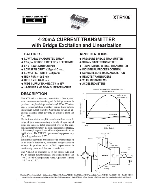
XTR106U中文资料
International Airport Industrial Park • Mailing Address: PO Box 11400, Tucson, AZ 85734 • Street Address: 6730 S. Tucson Blvd., Tucson, AZ 85706 • Tel: (520) 746-1111 • Twx: 910-952-1111 Internet: / • FAXLine: (800) 548-6133 (US/Canada Only) • Cable: BBRCORP • Telex: 066-6491 • FAX: (520) 889-1510 • Immediate Product Info: (800) 548-6132
©
1998 Burr-Brown Corporation
PDS-1449A
Printed in U.S.A. June, 1998
元器件交易网
SPECIFICATIONS
At TA = +25°C, V+ = 24V, and TIP29C external transistor, unless otherwise noted. XTR106P, U PARAMETER OUTPUT Output Current Equation Output Current, Specified Range Over-Scale Limit Under-Scale Limit ZERO OUTPUT(1) Initial Error vs Temperature vs Supply Voltage, V+ vs Common-Mode Voltage (CMRR) vs VREG (IO) Noise: 0.1Hz to 10Hz SPAN Span Equation (Transconductance) Untrimmed Error vs Temperature(2) Nonlinearity: Ideal Input (3) INPUT(4) Offset Voltage vs Temperature vs Supply Voltage, V+ vs Common-Mode Voltage, RTI Common-Mode Range(5) Input Bias Current vs Temperature Input Offset Current vs Temperature Impedance: Differential Common-Mode Noise: 0.1Hz to 10Hz VOLTAGE REFERENCES(5) Initial: 2.5V Reference 5V Reference Accuracy vs Temperature vs Supply Voltage, V+ vs Load Noise: 0.1Hz to 10Hz VREG(5) Accuracy vs Temperature vs Supply Voltage, V+ Output Current Output Impedance LINEARIZATION(6) RLIN (external) Equation KLIN Linearization Factor Accuracy vs Temperature Max Correctable Sensor Nonlinearity POWER SUPPLY Specified Voltage Range TEMPERATURE RANGE Specification Operating Storage Thermal Resistance 14-Pin DIP SO-14 Surface Mount VREF2.5 VREF5 VREF = 2.5V or 5V TA = –40°C to +85°C V+ = 7.5V to 36V IREF = 0mA to 2.5mA VREG TA = –40°C to +85°C V+ = 7.5V to 36V IREG I REG = 0mA to 2.5mA RLIN KLIN VREF = 5V VREF = 2.5V TA = –40°C to +85°C VREF = 5V VREF = 2.5V IO IOVER I UNDER IZERO CONDITIONS MIN IO = VIN 4 24 1 2.9 TYP MAX MIN XTR106PA, UA TYP MAX UNITS A mA mA mA mA mA µA µA/°C µA/V µA/V µA/mA µAp-p A/V % ppm/°C % µV µV/°C µV/V µV/V V nA pA/°C nA pA/°C GΩ || pF GΩ || pF µVp-p
- 1、下载文档前请自行甄别文档内容的完整性,平台不提供额外的编辑、内容补充、找答案等附加服务。
- 2、"仅部分预览"的文档,不可在线预览部分如存在完整性等问题,可反馈申请退款(可完整预览的文档不适用该条件!)。
- 3、如文档侵犯您的权益,请联系客服反馈,我们会尽快为您处理(人工客服工作时间:9:00-18:30)。
Subject to local technical requirements and regulations, availability of products included in this promotional material may vary. Please consult with our sales office. Information furnished by HAMAMATSU is believed to be reliable. However, no responsibility is assumed for possible inaccuracies or omissions. Specifications are subject to change without notice. No patent rights are granted to any of the circuits described herein. © 1998 Hamamatsu Photonics K.K.
PHOTOMULTIPLIER TUBE R106
TPMS1040E01JUN. 1998
HAMAMATSU PHOTONICS K.K., Electoron Tube Center
314-5, Shimokanzo, Toyooka-village, Iwata-gun, Shizuoka-ken, 438-0193, Japan, Telephone: (81)539/62-5248, Fax: (81)539/62-2205
U.S.A.: Hamamatsu Corporation: 360 Foothill Road, P. O. Box 6910, Bridgewater. N.J. 08807-0910, U.S.A., Telephone: (1)908-231-0960, Fax: (1)908-231-1218
Germany: Hamamatsu Photonics Deutschland GmbH: Arzbergerstr. 10, D-82211 Herrsching am Ammersee, Germany, Telephone: (49)8152-375-0, Fax: (49)8152-2658
France: Hamamatsu Photonics France S.A.R.L.: 8, Rue du Saule Trapu, Parc du Moulin de Massy, 91882 Massy Cedex, France, Telephone: (33)1 69 53 71 00, Fax: (33)1 69 53 71 10
United Kingdom: Hamamatsu Photonics UK Limted: Lough Point, 2 Gladbeck Way, Windmill Hill, Enfield, Middlesex EN2 7JA, United Kingdom, Telephone: (44)181-367-3560, Fax: (44)181-367-6384North Europe: Hamamatsu Photonics Norden AB: Färögatan 7, S-164-40 Kista Sweden, Telephone: (46)8-703-29-50, Fax: (46)8-750-58-95
Italy: Hamamatsu Photonics Italia: S.R.L.: Via Della Moia, 1/E, 20020 Arese, (Milano), Italy, Telephone: (39)2-935 81 733, Fax: (39)2-935 81 741
TPMSB0142EA
Figure 2: Typical Gain Characteristics
Figure 3: Dimensional Outline and Basing Diagram (Unit: mm)
TPMSA0001EA
TACCA0064EA
CHARACTERISTICS (at 25°C)
Parameter Typ.Min.Max.Unit
Anode Sensitivity Cathode
Sensitivity
Gain
Anode
Dark Current Time
Response
A/lm A/W A/W µA/lm mA/W mA/W %—nA nA ns ns 4003.5 × 1051.8 × 10550483522 at 210nm 8.0 × 106212.222100
——
25
———————————————
—1010——Luminous (2856K)Radiant Luminous (2856K)Radiant Quantum Efficiency after 5 seconds after 30 minute
Anode Pulse Rise Time Electron Transit Time at 340nm at 200nm at 340nm at 200nm MAXIMUM RATINGS (Absolute Maximum Values)
Parameter Value Unit Supply
Voltage
Average Anode Current Ambient Temperature
12502500.1-80 to +50
Vdc Vdc mA °C
Between Anode and Cathode Between Anode and Last Dynode
Supply Voltage: 1000Vdc, K: Cathode, Dy: Dynode, P: Anode
VOLTAGE DISTRIBUTION RATIO AND SUPPLY VOLTAGE
Electrodes Ratio K Dy11Dy21Dy31Dy41Dy51Dy61Dy71Dy81Dy91P 1DIRECTION OF LIGHT
108
107106
105
104
103
102
250300
400700100015002000
SUPPLY VOLTAGE (V)
G A I N
Socket (Option)(E678-11A)。