基于3D集成电路的测试技术
3D IC-TSV技术与可靠性研究
3D IC-TSV技术与可靠性研究摘要:对三维(3 Dimension,3D)堆叠集成电路的硅通孔(Through Silicon Via,TSV)互连技术进行了详细的介绍,阐述了TSV的关键技术与工艺,比如对准、键合、晶圆减薄、通孔刻蚀、铜大马士革工艺等。
着重对TSV可靠性分析的重要性、研究现状和热应力分析方面进行了介绍。
以传热分析为例,实现简单TSV模型的热仿真分析和理论计算。
最后介绍了TSV技术市场化动态和未来展望。
关键词: 3D-TSV;通孔;晶圆减薄;键合;热可靠性0 引言随着半导体制作工艺尺寸缩小到深亚微米量级,摩尔定律受到越来越多的挑战。
首先,互连线(尤其是全局互连线)延迟已经远超过门延迟,,这标志着半导体产业已经从“晶体管时代”进入到“互连线时代”。
为此,国际半导体技术路线图组织(ITRS)在 2005 年的技术路线图中提出了“后摩尔定律”的概念。
“后摩尔定律”将发展转向综合创新,而不是耗费巨资追求技术节点的推进。
尤其是基于TSV(Through Silicon Via)互连的三维集成技术,引发了集成电路发展的根本性改变。
三维集成电路(Three-Dimensional Integrated Circuit,3D IC)可以将微机电系统(MEMS)、射频模块(RF module)、内存(Memory)及处理器(Processor)等模块集成在一个系统内[1],,大大提高了系统的集成度,减小了功耗,提高了性能,因此被业界公认为延续摩尔定律最有效的途径之一,成为近年来研究的热点。
目前3D集成技术主要有如下三种:焊线连接(Wire-Bonding)、单片集成(Monolithic Integration)和TSV技术[2]。
焊线连接是一种直接而经济的集成技术,但仅限于不需要太多层间互连的低功率、低频的集成电路。
单片集成是在同一个衬底上制作多层器件的新技术,它的应用受到工艺温度要求很高和晶体管质量较差等约束。
基于典型集成电路的自动测试演示验证研究

计算机测量与控制!"#""!$#!%"!!"#$%&'()'*+%('#',&-!",&(".!!#")&!#收稿日期 "#"&&"$#$!修回日期 "#""#$#&%作者简介 闫丽琴!&*%)"&女&河北石家庄人&硕士&高级工程师&主要从事集成电路测试与验证方向的研究%引用格式 闫丽琴&王占选&冯建呈&等!基于典型集成电路的自动测试演示验证研究'+(!计算机测量与控制&"#""&$#!%")")&"))&$#"!文章编号 &',&()*% "#"" #%#")&#)!!-./ &#!&')"' 0!1234!&&5(,'" 67!"#""!#%!#$*!!中图分类号 89"*文献标识码 :基于典型集成电路的自动测试演示验证研究闫丽琴& 王占选& 冯建呈& 闫!静" 任朝旭&!&;北京航天测控技术有限公司&北京!&###(&$";北京微电子技术研究所&北京!&###,'"摘要 当前国产超大规模集成电路测试设备由于技术指标*工作可靠性*制造成本等诸多因素&在国内尚未得到大规模的市场应用$从集成电路的测试需求出发&给出了自研超大规模集成电路测试系统的总体架构组成&重点开展了基于典型集成电路的自动测试演示验证方法研究&并以国产某型超大规模静态存储器芯片作为演示验证的对象&利用自研测试系统完成了基于静态存储器芯片的自动测试演示验证试验$试验结果表明基于典型集成电路的自动测试演示验证方法和过程合理可行&能够为国产新研超大规模集成电路测试系统推广前的自动测试演示验证提供参考&同时可结合不同类型集成电路的测试需求深入应用到各类集成电路的测试过程%关键词 超大规模集成电路测试系统$演示验证$测试准备$测试开发$迭代调试$静态存储器测试/'+'*(01",=%&"#*&60O'+&G'#",+&(*&6",*,:['(6360*&6",K*+':",O@$60*.S,&'8(*&':!6(0%6&+`:^M4T42&&D:^bc G A2Y B A2&&Z>^b+4A21G E2P&&`:^+42P"&U>^c G A K Y B&!&;Q E4042P A E R K S7A1EI E A S B R E I E26d F K26R K O8E1G2K O K P J F K;&M6H;&Q E4042P!&###(&&F G42A$";Q E4042P=41R K E O E16R K241S8E1G2K O K P J/2S646B6E&Q E4042P!&###,'&F G42A"=>+&(*0&):67R E S E26&6G EG K I E X R E HW E R J5O A R P E5S1A O E426E P R A64K2!N M</"6E S642P E T B47I E26G A S2K6X E E2\4H E O J B S E H426G EH K5I E S641I A R3E6H B E6KI A2J L A16K R S&S B1GA S6E1G241A O S7E14L41A64K2&\K R342P R E O4A X4O46J&I A2B L A16B R42P1K S6&E61!/26G4S7A7E R&6G EK W E R A O O S6R B16B R E K L6G E S E O L5H E W E O K7E HN M</6E S6S J S6E I\A S P4W E2L R K I6G E6E S6R E T B4R E I E26SK L6G E426E P R A6E H14R1B46!=E A2\G4O E& 6G4S7A7E R L K1B S E S K26G E R E S E A R1GK L A B6K I A6416E S6H E I K2S6R A64K2A2HW E R4L41A64K2I E6G K HX A S E HK26G E6J741A O/F!:6O A S6&A1E R6A42 6J7EK L G K I E I A H E W E R J5O A R P E5S1A O E S6A641I E I K R J1G474S6A3E2A S6G E6E S6K X0E16S K L H E I K2S6R A64K2A2H W E R4L41A64K2&A2H6G E A B6K I A641 W E R4L41A64K26E S6X A S E HK26G E S6A641I E I K R J1G474S1K I7O E6E HX J B S42P6G E S E O L5H E W E O K7E H6E S6S J S6E I!8G E6E S6R E S B O6S S G K\6G A66G E 6E S6I E6G K HA2H7R K1E S S K L A B6K I A6416E S6H E I K2S6R A64K2A2H W E R4L41A64K2X A S E H K26G E6J741A O/F4S R E A S K2A X O E A2H L E A S4X O E&\G41G7R K5 W4H E S A R E L E R E21E L K R6G E A B6K I A6416E S6H E I K2S6R A64K2A2HW E R4L41A64K2X E L K R E6G E7K7B O A R4[A64K2K L6G E2E\G K I E I A H EN M</6E S6S J S5 6E I!=E A2\G4O E6G E R E S E A R1G1K26E261A2X E H E E7O J A77O4E H6K6G E A B6K I A6416E S67R K1E H B R E K L6G E K6G E R/F S\G E21K I X4242P6G E6E S6 R E T B4R E I E26S K L H4L L E R E26426E P R A6E H14R1B46S!'@A"(:+)N M</6E S6S J S6E I$H E I K2S6R A64K2A2H W E R4L41A64K2$6E S67R E7A R A64K2$6E S6H E W E O K7I E26$46E R A64K2H E X B P P42P$ <U:=6E S6B!引言集成电路测试贯穿于整个集成电路设计*生产*制造*封测以及应用全过程&对集成电路产业的发展起到了至关重要的作用%解决好集成电路测试问题&能有效缩短产品的研发周期&降低产品研制生产以及维护的费用&确保产品的性能质量与可靠性'&(%因此&集成电路测试的能力和水平是保证集成电路性能*质量的关键手段之一&也是集成电路测试产业的重要标志%国外集成电路自动测试系统的研究和研制工作开始较早&测试对象从较为简单的小规模芯片到如今各种超大规模集成电路&已经形成了一系列成熟的集成电路自动测试设备%目前&世界上先进的集成电路测试设备制造技术基本掌握在美国*日本等专业测试设备生产厂家手中&如泰瑞达*爱德万*科休等厂家%这些厂商在超大规模集成电路测试系统方面已形成了标准的体系架构&编制出软硬件架构及数据层的相关标准&研制出具有超大规模集成电路测试能力的自动测试设备&引领未来超大规模集成电路测试方向的发展'"(%我国集成电路测试研究已经取得了初步成效%近年来&得益于国家政策*资金等方面的大力支持&以及国内广阔的集成电路测试市场&我国集成电路测试产业发展迅猛&测试技术逐渐向世界先进水平看齐'$((%就高端高性能集成电路自动测试平台来说&国内市场依旧以国外测试设备为主导%国产超大规模集成电路测试设备由于技术指标*可!投稿网址 \\\!0S01O J3[!1K ICopyright©博看网. All Rights Reserved.!!计算机测量与控制!第$#""""""""""""""""""""""""""""""""""""""""""""""""""""卷#")"!#靠性*制造成本等诸多因素&目前在国内尚未得到大规模的市场应用')'(%本文针对国内超大规模集成电路的测试现状&一方面从集成电路的测试需求出发&分析集成电路测试的基本原理和测试要求&给出自研超大规模集成电路测试系统的总体组成和设计架构$另一方面详细研究基于典型集成电路的自动测试演示验证方法和过程$最后利用该方法在自研测试系统上开展静态存储器的演示验证试验&验证所述方法的可行性&为国内新研超大规模集成电路测试系统推广前的自动测试演示验证提供思路%C !集成电路测试需求分析集成电路测试是对被测器件进行检测&通过输出响应和预期结果的比较&确定或评估集成电路元器件功能和性能好坏的过程%当前集成电路测试按照测试内容进行分类主要包含)直流参数!-F "测试*交流参数!:F "测试*混合集成电路特性参数测试*功能测试等%C D C !直流参数G ! 测试需求直流参数测试主要测试器件有关电参数的稳定性能&一般按照被测器件设计规定&给被测器件电源引脚施加规定的电源电压后&基于欧姆定律给相应的数字引脚施加规定的电压或电流&测量被测器件规定引脚的电流或电压%通常利用99=C 或9=C 测量单元&采用加流测压或加压测流的方式对芯片的数字引脚进行参数测试$此外&利用-9<对被测器件电源引脚进行不同状态下的功耗测试%上述测试需同时保证测试数据的精准性',(%直流参数通常包含输出高-低电平电压!N .V -N .M "*输入高-低电平电流!//V -//M "*静态电源电流!<6A 641/---/F F "*动态电源电流!-J 2A I 41/---/F F "*输出高阻态电流!/.c V -/.c M "等'%(%C D E !交流参数=! 测试需求交流参数主要是针对芯片的时序参数进行测试&保证器件满足时序规格要求%一般通过运行功能测试的矢量!7A 66E R 2"序列来进行测试%测试的主要原理为在引脚输入端输入指定的时间边沿&特定时间后在引脚输出端检测输出的状态转换&并与预期状态进行比较'*&#(%交流参数包括建立时间!S E 6B 764I E "*保持时间!G K O H 64I E "*传输延迟时间!7R K 7A P A 64K 2H E O A J 64I E "以及其他时间参数'&&(%交流参数测试时&被测器件的引脚可能与测试设备的任意数字通道或者模拟通道资源连接&所以测试设备上一般需要具备时间相关量的测量单元%C D F !混合集成电路特性参数测试需求混合集成电路特性参数测试需求与集成电路类型密切相关%:-F 的静态参数用来衡量器件的静态性能&为实际量化特性与理想量化特性之间的偏差&动态特性通常是在频域范围内衡量器件的响应速度等特性$-:F 主要用于产生精确的电压*频谱信号以及连续波形等&其静态参数主要描述相对于每个输入码在输出端电压的表现&动态参数通常用来检验音频和视频-:F 的高频品质%其中&静态参数通常包括失调误差![E R K E R R K R "*增益误差!PA 42E R R K R "*微分非线性误差!-^M "和积分非线性误差!/^M "等$动态参数包括信噪比!<^U "*总谐波失真!8V -"*信噪比失真!</^:-"*无杂散信号动态范围!<Z -U "等'&"&$(%C D M !功能测试N %,0&6",*.O '+& 需求功能测试是芯片设计验证阶段的重要一环&主要目的是通过测试过程让被测芯片在一定的时序下工作&充分暴露其逻辑电路的问题&进而反馈电路的设计缺陷%其实现过程主要借助于测试矢量数据&对被测芯片引脚施加预先设定的激励&检测输出引脚的响应与预期响应是否一致%功能测试是对被测器件内部数字或者模拟电路的行为测试&需根据不同类型的集成电路分别处理%E !自研超大规模集成电路测试系统总体组成根据上述集成电路测试需求分析可知&测试系统是提供源表*信号发生器*数字矢量发生器和其他软硬件组成的集合体&通过主控计算机结合自动测试软件控制测试系统完成被测集成电路产品的测试工作%自研超大规模集成电路测试系统的总体架构组成如图&所示%图&!测试系统总体架构组成测试系统硬件主要包括主控计算机及外设*硬件模块资源以及测试接口单元%其中&主控计算机作为整个测试系统的控制中心&通过9@/E 高速总线控制接口与硬件资源进行总线通讯'&(&)(%硬件资源包含具备9@/E 接口的各种功能集成板卡&如设备供电电源-9<*数字测试模块*精密测量单元9=C *模拟测试模块*交直流源和测量仪表等%测试接口单元采用模块化接口组件的弹性对接方式&通过对接测试接口板&实现系统硬件资源通道与被测芯片的引脚连接%测试软件安装于主控计算机&主要实现测试矢量的生成和芯片测试流程的开发&生成测试程序数据流&自动完成测试软件与测试系统仪器之间的数据和指令交互&同时开展测试过程监控和测试数据的收发工作&并完成测试结!投稿网址 \\\!0S 01O J3[!1K I Copyright ©博看网. All Rights Reserved.第%期闫丽琴&等)""""""""""""""""""""""""""""""""""""""""""""""""""""基于典型集成电路的自动测试演示验证研究#")$!#果数据的记录%在芯片测试过程中&一方面进行测试过程的可视化数据调试&另一方面可对测试结果进行数据回放和分析'&'&,(&进行数据的离线处理%该自研超大规模集成电路测试系统采用高性能9@/E 高速测试总线的控制方式&遵循测试技术最新的集成架构&具有较强的扩展性和灵活性%该测试系统是针对数字类*模拟类和数模混合类等集成芯片的测试系统&系统硬件资源中的数字测试模块攻克了高速率多通道数字信号发生和分析技术&实现高端仪器的国产化$测试软件可实现跨平台运行&支持<8/M !S 6A 2H A R H 6E S 6426E R L A 1E O A 2P B A P E &标准测试接口语言"和<8-Z !S 6A 2H A R H 6E S 6H A 6A L K R I A 6&标准测试数据格式"标准&使得集成电路设计数据和测试系统能够无缝连接&实现数据共享机制'&%&*(%该测试系统建立了一套完整的软硬件体系&能够有效提供集成电路测试所需的测试资源&实现集成电路的功能测试*交直流参数测试等%F !基于典型集成电路的自动测试演示验证过程基于典型集成电路的自动测试演示验证基本流程如图"所示&主要包含测试准备*测试开发和迭代调试$个过程%图"!基于典型集成电路的自动测试演示验证流程框图F D C !测试准备过程测试准备过程开展典型集成电路测试前的准备工作&主要针对集成电路测试要求进行测试计划说明&判断所要测试的集成电路性能参数&明确待测产品的特点*频率*功耗*引脚数等详细信息&明确测试条件&进行测试需求分析&合理配置测试系统资源&确定芯片引脚与硬件测试资源之间的映射关系&制定详细的测试方案&为后续测试开发和迭代调试奠定基础%F D E !测试开发过程测试开发过程首先根据芯片封装特性和引脚映射关系进行<K 13E 6插座和测试接口板的设计开发%为了使被测集成电路和测试系统之间建立牢固*可靠和低损耗的电气连接&需要针对每类集成电路定制测试插座和测试接口板%其中&测试插座是整个测试系统中不可或缺的组成部分&尤其是在高速*高精度*大电流的电路测试中%根据电路的封装形式设计插座类型&固定方式一般采用焊接型或螺丝紧固型&设计加工好的插座安装在测试接口板上%设计测试接口板前需进行全面仿真和综合设计&优化布局*布线&并兼顾电磁屏蔽设计&测试接口板的质量直接关系到后续所有的测试质量&否则会严重干扰被测电路的测试信号%自研超大规模集成电路测试系统采用集成电路测试行业的<8/M 标准测试接口语言作为测试矢量数据的描述语言%测试矢量生成过程主要利用智能转换软件将集成电路的仿真数据文件或设计数据文件转换为符合<8/M 标准的时序和矢量文件&经综合后生成统一格式的<8/M 测试矢量文件%测试矢量生成方法如图$所示%图$!<8/M 测试矢量生成方法测试系统的存储深度有限&当集成电路的测试矢量超过系统矢量存储深度&测试将无法完成%另外&当测试矢量数据较大时&每次向系统导入以及编译矢量过程都会占用较长的时间&不便于测试程序的调试%同时&实际调试过程也会占用较长的时间&测试成本较高%因此&对测试矢量进行一定的优化&能够有效减少测试向量的存储空间&降低测试时间%矢量优化一方面从数据压缩角度进行&降低数据存储量$另一方面从矢量排序方面优化&降低测试时间'"#"&(%优化后的测试矢量需经过测试系统的专用矢量编译软件&编译为面向系统硬件的二进制数据文件&从而快速生成供测试系统数字测试模块使用的二进制测试矢量数据%测试流程是在自动测试软件中开发符合集成电路测试逻辑的一系列测试序列数据&包含电源*电平*矢量*84I 42P 时序*-F 参数*测试项*测试Z O K \等配置信息和过程信息'""(&并确保测试程序能够正常下载到测试设备%F D F !迭代调试过程测试程序开发完成或部分完成后&需要利用实际的集成电路来进行测试过程的试运行%测试调试过程中出现各种意外情况非常常见&需要根据测试系统返回的错误现象和Z A 4O S 信息判断问题出现的原因&定位是参数配置错误&还是测试激励仿真错误&甚至可能是接口板设计错误或者芯片本身的问题等%测试程序的迭代调试优化是测试电路测试无法省略的过程%测试程序迭代优化流程如图(所示%M !静态存储器自动测试演示验证试验本文以国产某型超大规模静态存储器芯片作为试验对!投稿网址 \\\!0S 01O J3[!1K I Copyright ©博看网. All Rights Reserved.!!计算机测量与控制!第$#""""""""""""""""""""""""""""""""""""""""""""""""""""卷#")(!#图(!测试程序迭代优化流程象&利用自研超大规模集成电路测试系统开展自动测试演示验证试验&静态存储器芯片的自动测试演示验证如图)所示%图)!静态存储器自动测试演示验证框图M D C !测试准备所选取的国产某型静态存储器芯片为一款高性能*大容量<U :=&数据位宽$"位&存储器容量为)&"a e $"X 46&接口兼容F =.<输入输出电平&具备双向三态数据总线&且电路为异步操作存储器&不需外接时钟%器件通过片选信号)及读-写控制信号N 实现器件的写操作$通过片选信号)*输出使能信号S 以及读-写控制信号N 可实现器件读操作%芯片为(裸芯片封装&每裸芯片的容量为)&"a e %X 46%器件工作状态真值表如表&所示%表&!存储器工作状态真值表输入输出S N )/-.模式工作模式@@&-?2!,)#"三态待机@##-?2!,)#"数据输入写操作#&&-?2!,)#"数据输出读操作&&#-?2!,)#"三态读操作&数据端口三态!!注)@m -K 2661A R E $2代表裸芯片序号%<U :=存储器测试包含供电功耗测试*直流参数测试*交流参数测试和功能测试'"$(%其中&供电测试利用测试系统的-9<模块&对存储器芯片的内核电路*外围/.供电&分别完成芯片待机和工作状态下的功耗测试%直流参数测试主要包含输出高-低电平*输入漏电流*三态输出漏电流*待机和工作电源电流等%利用-9<模块完成电源功耗测试&采用数字测试模块的99=C 功能进行其他直流参数测试&以保证测试数据的精度&必要时通过施加测试矢量配合测试完成%交流参数测试包含存储器特定的读-写周期*建立时间*保持时间等&结合测试矢量&采用参数搜索的测试方法&通过对全局变量按照一定规律变化的赋值获取时间参数的测试结果%对于大规模存储器电路的功能测试&需要有大容量的矢量存储深度&同时能够实现存储器测试的算法向量%在测试向量方面应提供包含全#全&向量&棋盘格!1G E 13X K A R H "测试向量*=A R 1GF 测试向量等&以及通过基本向量算法衍生出来的改进算法&进一步提高存储器故障模型的测试覆盖性'"(")(%根据上述测试条件和测试方案&结合存储器产品手册中的引脚定义和引脚属性&明确芯片引脚与系统硬件资源中数字测试模块和-9<供电模块之间的接口映射关系&如图'所示%图'!存储器引脚与硬件资源之间的映射关系M D E !测试开发(;";&!测试插座和接口板设计开发测试接口板实现被测存储器芯片引脚与测试系统资源通道之间的连接桥梁&确保测试信号传输的完整性%针对该存储器芯片设计专门的测试接口板&为了节省演示验证过程测试接口板的设计成本&采用子母板的设计形式%其!投稿网址 \\\!0S 01O J3[!1K I Copyright ©博看网. All Rights Reserved.第%期闫丽琴&等)""""""""""""""""""""""""""""""""""""""""""""""""""""基于典型集成电路的自动测试演示验证研究#"))!#中母板设计为通用测试接口板&实现系统硬件资源的适配转接&子板转接存储器芯片测试所需的硬件通道资源&并安装存储器芯片测试的专用<K 13E 6测试插座%(;";"!测试矢量生成*优化和编译根据测试需求&测试系统提供基于<8/M 标准的存储器测试矢量算法生成工具&包含全#全&*正反向棋盘格和=A R 1G 矢量等矢量生成算法%存储器测试矢量主要通过引脚来侦测芯片制造过程中出现的缺陷&故障模型要尽可能考虑周全&但是测试时间仍然不能够过长&因此&通过不同算法的选择来完成测试矢量排序方面的优化&减少测试时间&并利用系统的专用编译器将基于<8/M 格式的测试矢量文本文件编译为测试系统数字测试模块可以正确识别的二进制数据文件&进一步提高系统的测试效率%(;";$!测试程序开发和下载存储器测试流程主要包含连接性测试*功能测试*直流参数测试以及交流参数测试等&根据不同参数的测试原理&在自动软件平台根据测试准备过程的测试方案开发存储器的942引脚定义*9A 13A P E 映射*9K \E R 供电*M E W E O 电平*84I 42P 时序*直流参数*9A 66E R 2矢量等配置项&组织不同的测试项目&建立存储器芯片的测试流程%最终将编译无误的矢量文件和测试程序下载至系统内部的功能板卡&为存储器芯片测试程序的快速运行做准备%M D F !迭代调试迭代调试是一个反复运行测试程序的过程%静态存储器自动测试演示验证试验是在确保测试接口板设计正确和待测存储器芯片正常工作的前提下开展迭代调试%首先通过反复调试运行单个测试项目&如输入漏电流*输出高低电平*电源功耗*各算法矢量作用下的功能测试等&完成各个测试项目的调试&根据测试项目运行结果定位错误原因&如参数超限*功能矢量Z A 4O 等&通过不断修改优化测试程序的配置项参数&如电平*时序以及矢量数据文件等&反复运行单个测试项目的测试&确保测试项目的稳定性$其次在单项测试通过的基础上按照相同的迭代调试原理分别开展部分以及整个存储器测试流程的调试&验证测试流程的可执行性$最终固化存储器芯片测试程序&完成基于静态存储器芯片的自动测试演示验证试验过程%表"为运行经过迭代调试后的存储器芯片测试流程主要典型参数结果数据与芯片电参数表规定的数据范围对比%根据对比结果可知&利用该自研超大规模集成电路测试系统开展某型静态存储器芯片自动测试演示验证试验&所有测试试验结果均在电参数表要求范围内&满足要求%R !结束语随着集成电路工艺的不断发展&国内外市场对于超大规模集成电路芯片的要求越来越高&必须通过全方位的测试验证其强大功能和高可靠性%针对国内超大规模集成电路的测试现状&通过静态存储器的自动测试演示验证试验&有效验证了基于典型集成电路的自动测试演示验证方法和过程&一方面为国内新研超大规模集成电路测试系统推广表"!存储器芯片典型参数测试结果与电参数表要求范围对比序号测试参数名称实测结果电参数表要求范围是否满足要求&!输出高电平N .V 最大值)$!""**%#N最小值)$!"#)"'&N 上限)...下限)"!'(N 满足"!输出低电平N .M 最大值)$$"!*(',,,I N 最小值)"'(!"%"""'I N上限)#!''N 下限)...满足$!输入高电平N /V 设置N /Vm "!$&N 时&功能测试向量9A S S 上限)...下限)"!$&N 满足(!输入低电平N /M设置N /Mm#!**N 时&功能测试向量9A S S上限)#!**N 下限)...满足)!输入高电平电流//V 最大值)($'!$,'*)#2:最小值)$'(!&&&$&)2:上限)&$:下限)]&$:满足'!输入低电平电流//M 最大值)($(!'',*%&2:最小值)$,$!%,'*),2:上限)&$:下限)]&$:满足,!三态输出高电平电流/.c V 最大值)(#)!$,&#%"2:最小值)$'%!,(***(2:上限)&$:下限)]&$:满足%!三态输出低电平电流/.c M 最大值)(#&!""#,&,2:最小值)$'(!)**'##2:上限)&$:下限)]&$:满足*!内核电源工作电流%&=V ["$!'"&(',I :上限),#I :下限)...满足&#!/.电源工作电流%&=V [#!&")$%('I :上限)#!$)I :下限)...满足&&!内核电源工作电流%)%!%=V [&%$!(,"$,'I :上限)""#I :下限)...满足&"!/.电源工作电流%)%!%=V [(!$(")%&I :上限)&&I :下限)...满足&$!数据读取时间6:N ?N&$!')$(&%2S上限)&,2S 下限)...满足&(!控制有效输出使能时间6b M ?N(!(&$(),2S上限),2S 下限)...满足&)!功能测试全#)9A S S $全&)9A S S棋盘格)9A S S 反向棋盘格)9A S S =A R 1G F 测试)9A S S全#*全&*棋盘格*反向棋盘格*=A R 1G F 测试矢量全部通过满足前的自动测试演示验证提供思路&另一方面可结合不同类型集成电路的测试需求将该方法深入应用到各类超大规模集成电路的测试过程中%参考文献'&(宋铁生!集成电路测试技术的应用研究'+(!电子测试&"#&,!&'")*'*,!!下转第$#"页"!投稿网址 \\\!0S 01O J3[!1K I Copyright ©博看网. All Rights Reserved.。
3D封装集成电路测试挑战的ATE解决方案

ATE solutions to 3D-IC test challenges The rea diness of Advantest’s V93000Scott Chesnut scott.chesnut@Robert Smith robert.j.smith@Florent Cros florent.cros@Lakshmikanth Namburi lakshmikanth.namburi@Advantest AmericaSan Jose, California USAAbstract—Three dimensional integrated circuits (3D-IC) require that automatic test equipment develop capability to address the challenges brought on by these structures.Such capability is found in test solutions which provide multiple clock domains, granular hardware porting per 3DIC layer, powerful test languages to control this hardware and collaborative software development environments.Advantest’s introduction of clock domain per pin, multi-port, concurrent test, and protocol aware software, MEMS probes, and SmarTest program manager address the test challenges of 3DIC in an effective effectively. They allow production solutions to be architected to the degree of granularity required by the development teams.Keywords—Protocol aware, Clock domain per pin, multi-port hardware, concurrent test framework, Protocol aware, SmarTest program manager, PLL Keep Alive, 3DIC TSV, 25uM pitch, MEMS Probes, ATE, BIST, JTAG, Pico Ampere Meter, interposer, spatial translation, MEMS, planarity, probes, cantilever, beam.I.I NTRODUCTION3D chips are multi-system entities whose test challenges dwarf those presented by yesterday’s System in a Package (SiP) and/or System On a Chip (SOC). Substantial infrastructure must be readied in order to position any Automatic Test Equipment (ATE) to succeed in a production test environment. A good approach to understanding what the real challenges are would be to eliminate those with already known solutions.Past efforts to reduce test time, increase test coverage, and coordinate the software efforts of large groups of test engineers have solved 2D related production test problems. While these solutions had been developed for reasons other than 3DIC/TSV production test, we find they may lend themselves well to the task. Many of the perceived 3DIC/TSV test problems actually already have solutions. What follows is a description of how the existing features of Advantest’s V93000 might address many of these challenges.A.Test Program Software Maintenance – SmarTest ProgramManager.Historically, a chip had one function. As more functions where added they became systems on a chip and then the migration to system in a package occurred. 3DIC systems in a stack add even greater complexity.Whether 3D stacks are assembled from Known Good Die (KGD) or Pretty Good Die (PGD) it can be assumed that “some” level of test will occur at both the chip level and then the stack level. Without assurance that chip layers are somewhat functional, a single layer’s defect can result with failing of the entire stack. Test costs become prohibitive as many good die are lost due to a single bad layer.Testing die before and after stack assembly requires use of variations of the same test program. One program version is used for the single die, another for the assembled stack. This is because test at the chip level will target its subcomponents while test at the stack level will exercise mission mode system level performance.It is likely that the same program be used for both activities with the difference being in how it perceives its current purpose. That is, a well architected test program can receive instructions from an operator or prober/handler and branch into chip or stack level test.Whether testing PGD, KGD, on the chip or stack level, use of the same program to test both reduces the correlation burden between chip test and assembled stack test. Proper maintenance of these program variations will require tighter book keeping than in the past.3D structures, being built from multiple separate chip layers have associated with them legions of test, product and design engineers responsible for performance of each layer. Large groups of people who, while in the past never had reason to collaborate, in the future will find it absolutely necessary. Since each layer represents man years of test development effort, the test programs of each engineering group will haveto be integrated into a single large master test program whose purpose is test the entire stack or portions of it as it is built.Collaborative test development software packages must enable graceful checking in and out of test program modules with a minimum of inter-group interaction and/or miscommunication. Ideally, it would also address multi-platform customer concerns because the intellectual property of a given test is expected to come from bench data, EDA tools, Verilog simulations and/or competing testers.A method of handling this task is found in Advantest’s SmarTest Program Manager. While the product has many features which ease program generation, version control, translation, and test time reduction, it also allows effective collaboration between any number of engineers who independently debug, modify, and re-integrate changes into the master test flow. Already a highly mature product SmarTest Program Manager lends itself well to the task of 3DIC test software development, integration and maintenance.B. Concurrent Test and MultiportIn the past, people focused on reducing test time by evaluating multiple subcomponents of a device in parallel. The more that could be run in parallel, the greater the test time savings. Older testers having single clock domains and primitive synchronization software had difficulty addressing this challenge.The Advantest V93K enables 128 separate clock domains for digital/analog/RF testing. Separate clocking makes possible the Multiport and Concurrent test features of the V93K hardware and software. This highly granular resource control allows mission mode test to be accomplished. Improved test coverage occurs because each DUT core can interact autonomously and asynchronously with the tester if actually operating in the target application.The Advantest V93K enables 128 separate clock domains for digital/analog/RF testing. Separate clocking make possible the Multiport and Concurrent test features of the V93K hardware and software. This highly granular resource control allows mission mode test to be accomplished. Improved test coverage occurs because each DUT core can interact autonomously and asynchronously with the tester as actually operating in the target application.While this feature has been in use on 2D products for years, its usefulness becomes apparent during 3DIC stack assembly test. Assuming that access to the TSV pads are on the top of every layer to be assembled, and assuming that the probe technology used to make contact to them exists, we might see the bond/build up process as shown in the figures below.During 3DIC assembly, the signal type and speed of the accessible TSVs of each layer will be different. The TSV signals exposed on the top of the interposer layer will differ from those exposed on the top of the CPU layer. Similarly, those of the CPU layer will be different than those of theSRAM layer, and so on. A single master test program can test separate layers as they are placed on the growing stack. This master test program will use each of the many configuredFigure 2 SmarTest Program Manager facilitatescollaborative program development.Figure 3 Concurrent test of IC cores by converting serial tests to parallel through the use of concurrent test framework and multiport configurable hardware.Figure 4 Step 1: Port A of the tester resource set is usedto interrogate the first stack layer – the interposer.Figure 5 Step 2: Port B of the tester resource set is used to interrogate the second stack layer - the CPU. Figure 6 Step 3: Port C of the tester resource set is used to interrogate the second stack layer – the SRAM.ports, each architected to serve the needs of every layer. In this way as layers are bonded on the stack and as the profile of the accessible signal sets change, a new test program need not be loaded into the tester. Multiple separate programs will not be needed.C. Clock Domain per PinAdvantest’s Multiport allows the hardware assignment granularity required to test discrete 3DIC layers and cores within each layer. As mentioned previously, another such feature is clock domain per pin capability of Advantest’sPS1600 and PS9G digital pins. Such functionality allows each layer or layer sub function to operate in any of up to 128 total asynchronous clock domains, each supporting independent periods resolved to 3nS. This can be considered a requirement for future 3DIC designs because the integration of multiple IP cores on stack layers will require multiple clockfrequencies/domains. Mission mode setup and operation becomes an issue as more layers of the stack are assembled because direct access to sunken layers will become obscured. The only way to operate the partial stack will be if the ATE can achieve this functionality. Hence ATE targeting 3DIC test needs to be a flexible multi clock domain instrument as well as one supporting Multiport.As seen in Fig. 7, the Advantest test equipment can be configured to operate each individual layer at its required asynchronous clock rate. Stack layer clock rates will have to be provided whose frequencies are dissimilar to the point of only being fractionally related to those around them. Multiple free running clocks will have to be provided to different layers again at different rates. PCI express, PXI, SLIM bus, etc. protocols will be expected to run simultaneously on different parts of digital hardware while unrelated RF/mixed signal activities occur autonomously as well. Data bus rates of multiple layers can be expected to have unique timing requirements unto themselves.D. Protocol Engine per PinAs the 3D chip is built and tested, bottom layers will have been designed to communicate with others which are not yet present. Again, this type of communication is expected to be done in mission mode. A tester will have to become the“surrogate stack” until future layers are assembled. It will be required that the ATE act to perform the virtual functions of the remaining un-built stack layers in order to facilitate the mission mode testing of the targeted layer as well as the layers underneath it. It becomes necessary to use protocol aware to make the stack “think” it is talking with the rest of itself even though it’s yet not there. A tester implementing protocolaware allows the tester to act as the remaining un-built portion of the stack.But physical challenges occur as the stack layers are built up. These stem from the fact that the X-Y locations of a given signal set will change from layer to layer. That is, pads whose purpose was to send/receive PCIE signals at topological location A on layer 1 may be found at location F on layer 2. This is generally known as the “spatial translation” of a given signal set from layer to layer.To compound the problem, on layer 2 the pads at location A may be required to perform I2C protocol not PCIE. Normally, to accommodate this would require a separate probearrangement for each layer meaning a separate probe card for each layer and a separate way of handling the protocol change. Alternatively, since the V93000 port granularity allows forFigure 8 As stack layers are added, the tester must mimic the function of future, not yet present layersEarly in the assembly/test processLater in the assembly/test processreassignment of digital pins from one port to another in a dynamic fashion, this exception is handled. Probe card pins which test I2C on one layer can be reconfigured as PCIE on another. This is because the V93000 supports the Protocol Engine per pin which means the same pin can test eitherprotocols (or any other for that matter) on the same probe pin (same X-Y layer location) across all of the layers.Unfortunately, if the type of spatial translation is occurring between layers and moves from digital to RF or mixed signals, this solution falls apart because the function of the testerresource changes entirely thus requiring reassignment of probe card wiring to a different tester resource or a local relay implementation. Possible solutions to this problem are:1. Develop a JEDEC (Joint Electronic DeviceEngineering Council) standard which enforces strict TSV signal type assignment rules. But this will require all layer vendors to observe definedconventions. As of the date of this writing, JEDEC has yet to develop a complete standard.2. Design every tester pin to accommodate every signaltype: RF/Power/Mixed Signal/Digital. This is an impractical, expensive, and multi-man year solution to develop.3. Re-route probe cards for every layer. This requiresmultiple separate probe cards - one for every layer which would be expensive.4. Use interposers to perform the spatial translation.While this adds to the assembly burden, it is aflexible solution which could handle physical layout exceptions. But as such requires that all interposers be individually tested.The most practical currently available solution to this problem would be to introduce interposers between layers to route signals of a given type to a region of the probe card wherethese tester resources have already been assigned. In this way, repositioning of the probe arrangement by way of another probe card is not required (eliminating the requirement for multiple probe cards and the time to change them).E. InterposersThere has been recent focus on the use of interposers toperform the intra-layer spatial translation. This is so not only for the reasons specified above (to avoid spatial translation of digital to RF signals and to address mechanical pitchmismatches) but also because use of them relinquishes chip designers from the responsibility of routing signals to the TSV x/y locations required by the next/previous layers of the stack. While the JEDEC consortium outlines the standard JESD49A, which suggest conventions where by these designer might compromise their efforts it is not complete; a simpler solutionmay the use of interposers.The word “interposer” comes from the Latin, interpōnere,meaning 'to put up between'. In the context of 3DIC test an interposer will perform the spatial translation of signals coming from one layer’s X/Y positions to that of the next layer. The interposer will be “put in between” layers in order to route signals using conductive paths.Interposers can be used to route signals of a given nature toprobe card pins which are already assigned to that type ofFigure 12 Simplified Interposer Concepts. Signals from bottom sidebeing routed to a different location on the top. Same side signalsbeing routed to different locations.Figure 9 PCIe port being tested on layer 1 at locations A.Figure 10 Locations A on layer 3 is tested as a memory interface. Location F now tests the same PCIe pins as on layer 1 now spatially translated from locations A on layer 4.Figure 11 Locations A tests I2C protocol.Location F interfaces with PowerManagement and is concurrently tested at anasynchronous rate using a differentcommunications protocol.X-Y Locations ―A‖ test functionfrom PCIe to Memorytester resource signal (RF/mixed signal/digital/power). This eliminates the requirement to swap probe cards during intra-layer production test of the stack.The number of TSVs found in future 3D devices is expected to be large - hundreds or thousands on top and bottom of each layer. The conductive traces on interposers will be comprised of very small geometries and tax the limits of mechanical fabrication tolerances. Because of this, a great number of the traces (if not all) are to be tested if for no other reason than to check process variations.To test interposer trace connectivity in production will require more than just continuity. The current carrying capability of each trace is expected to be very low – too low for standard ATE parametric instrumentation to be able to resolve. While Time Domain Reflectometry (TDR) techniques can be used to validate/characterize line length, continuity, and possibly impedance, it cannot verify current carrying capability(conductance). The Advantest Pico-amp Measure Card, can do all of these. Line length is verified by resistivity per cubic millimeter and knowledge of ideal trace volumetric and or cross sectional dimensions.It is a requirement that interposer test be as thorough as that found in Known Good Die. By the time an interposer is to be attached to the stack it must be 100% functional. It will make sense to bond the interposer on the die layer without testing the TSV it lays on. All that will need to be evaluated will be the bonding process. This occurs during the normal course of that layer’s mission mode test.The described approach solves the spatial translation problem associated with digital signals positioned on the RF tester resource x/y locations on the probe card. If signals of a given type (RF, digital, mixed signal) are routed to pre assigned probe card regions where these tester resources are already connected, the requirement of having to probe RF signals withdigital hardware is eliminated. The interposer will always reroute the signal to the appropriate area of the probe card matrix where the required tester resource is assigned.So with the use of a fully tested known good interposer, the problem of spatial translation to conflicting tester resources is solved. Probe is done after interposer assembly. Contact to the relevant TSVs by the proper tester resource is achievedbecause such signals are routed to quadrant containing probes connected to the appropriate tester resource.Because the use of the interposer allows routing of signals to the locations of dedicated probes, could we conclude that issue is solved.But designers may not assign next layer TSV locations at the same location as the interposer probe locations. This means that the interposer must perform two purposes: 1) to route signals to the location of dedicated probes and 2) to route signals to the location of the next layers input/output TSVs. Therefore the interposer design mentioned in Fig. 14 must change to resemble that of Fig. 15.Here the input and outputs of the interposer are located differently than that of the probe points. Placing the probe points on signal traces as suggested creates new but tractable problems. The first is that, if left exposed, the probe points might contact TSVs on the layer above it. There might be anyFigure 15 Interposer traces which contain probe card pads whose location is different than the signal output/inputs introduce reflection stubs.Figure 13 Actual Interposer Implementation. [1]Figure 14 Interposers can be used to reroute signals of a given type to predetermined probe card location where a tester resourceassignment conversion is observed. This methodology eliminates the requirement to rearrange tester resource assignment on the probe card by way of the use of another probe card during production test.number of solutions to this problem, for instance, by locating the probe points in inert locations of the next stack layer.The next problem is that of reflective stub introduced by the trace path stubs to the exiting TSV. These stubs can create reflections which could corrupt the signal integrity at the probe point. This can be solved based on knowledge of the frequency of the signals being probed. Given that the stubs are expected to be very short, (less than 3 mm) and that typical RF transmission frequencies (the highest expected in such anapplication) are approximately 5GHz, if the dielectric constant (Er) of the interposer where chosen to be as low as possible, interference from such reflections can be considerednegligible. The same can be said for high speed digital signals except that their susceptibility to reflective perturbations is far less because of the greater noise margin inherent in digital signals.F. 3D, Through Silicon Vias (TSVs) and Precision Parametric TestingThe benefits of “die stacking” into 3D structures are higher reliability, lower power consumption and higher speedperformance. This stacking will require individual die being very reliable and have very high test yield. Ideally, a single manufacturer would have complete control over each die’s electrical quality, performance, and physical construction. This would insure that stacking would have a very high probability of a fully functional product.However, in reality, it is unlikely a single company would manufacture all die layers required to make a complete 3D system product. Several manufacturers are expected tofabricate all of the different layers. If a die is added to the 3D stack which does not meet the stringent performancerequirements, a non-function 3D product would result. Worse would be a reliability failure in the field of the finished product. This would result in recalls and lost revenues.As TSVs pass through a die they could pass by critical active areas and cause undesirable effects in performance. It will be important that all signal routings using TSVs be well plannedand understood across all vendor designs in 3D systems.TSVs will also create new device leakage and dielectric paths. Resistance and capacitive paths created by these TSVs willhave to be monitored and understood. Thousands of new TSV are to be added as each new layer is added to the stack. Each such path could affect the stack performance and powerconsumption. Hence signal and power paths will require high accuracy testing. Engineers must be able to measure lowleakage current levels in order detect possible defects before a new die is added to the stack. The same will hold for total system leakage after the stack has been assembled.Having precision measuring ability early in the manufacturing process is a requirement as device process teams will monitor TSV diameter, height and oxide thicknesses as a function of signal and power paths. Checking thousands of TSVs or just a sampling of critical ones will prove nontrivial.Hence parametric testing will be required during theevaluation of individual die and during the die stack up phase. Quality precision parametric measurements of the TSVs, bumps, both C4 and micro C4 is key to successful 3D manufacturing. Today’s testers provide some precision parametric testing capability on a limited amount of pins. Using this solution is unacceptable as it would lead to a two pass test strategy unless a highly accuracy parametric parallel test solution is available.A highly parallel test solution would provide the ability to measure nano-Ampere (nA) or pico-Ampere (pA) accuracy and accurate resistance measurements in the milli-ohm ranges across many pins in parallel. Advantest’s precision, highly parallel DC test solution provides a solution. The Advantest pico-Ampere option provides 100 pins of precision nA and pA current measurement ability in true parallel fashion.Figure 16 3D stack die yield as a function of number of die in stack. Figure 17 3D TSV process capacitance, resistance, and leakage paths. Figure18 Block diagram of a single channel of the Advantest 93000 pA tester.Fig. 18 is a block diagram of a single pin’s architecture of the 100 pin Advantest highly parallel precision parametricmeasurement system. Each of the 100 pins is identical and can be independently programed on a per pin basis. One pass testing of digital data, standard PPMU, and precision PA parametric provides true one pass testing at wafer sort.G. Micro Electro Mechanical System (MEMS) Probes If 3D devices become more prevalent, wafer probes andprobing techniques need to be re-evaluated. Thinned devices used in 3D stacking will need to be thoroughly tested to ensure high reliability before they can be used in a system leveldevice. These thinned cannot withstand the force and pressure exerted by conventional probes. This force and pressure is magnified as device pitch and technologies shrink anddensities increase. Conventional probes can cause damage by destroying devices at wafer level or worse by physically overstressing a die or TSV structure. This overstressed die can cause a failure of the 3D stack device over time. Probe contact planarity across a TSV arrays is essential for uniform contact resistance.Conventional metal MEMS probes can use vast areas of space(millimeters of length) in their construction to achievecompliance. These construction techniques will limit their use because of pitch and required higher densities which may cause probe misalignment.Advantest’s MEMs probe solution addresses many of these problems. Using multi-level metal MEMS processing, microlithography and through-mold electro-depositiontechniques, Advantest creates MEMs probes whose electrical and mechanical characteristics more closely match thatrequired by these challenges. Shown below in Fig. 21 is a completed Advantest MEMS probe photo.This fabrication process allows for high levels of consistent planarity from tip to tip as well as across the complete MEMS probes structure. Utilizing these techniques Advantest MEMS probes can be consistently fabricated to exacting standards. This tip to tip planarity process translates into much better compliance and less overdrive stress on thinned wafers.Another benefit of this is consistent path contact resistance as deflection is consistent across the probe array.Figure 21 Scanning Electron Microscope (SEM) image of probe array showing high level of view of fabricated probe and sub-micron tip to tip planarity.H. ConclusionAlthough the number of 3DIC TSV devices in production around the world is very small, if it were to ramp suddenly, test engineers might find themselves without knowledge of available solutions. What has been described are the features of Advantest’s V93000 and how they might address many of the 3DIC TSV test challenges as viewed from the perspective of system experts.We have described how, using the currently available and mature features of the Advantest 93000 test system, theproblems associated with software revision control, multiple clock domains, multiport and concurrent test usage are provided by this tester platform. Use of the Pico Ampere Meter to thoroughly test interposers may be a requirement because they cannot be tested fully once assembled on the stack. The use of interposers as described will eliminate the necessity of swapping probe cards during production as stack layers are assembled, because spatial translation of layer signals to the appropriate tester resource is achieved. Also utilizing MEMS probe designs will allow testing of thinned wafers with minimal pressure allowing test of structures more consistently and more repeatedly. This will translate into higher and more consistent wafer and die yields.R EFERENCES[1] Image obtained from: MEMS Journal:/2010/04/overview-of-tsv-process-options.htmlFigure 19 Wafer Thinned to 50umFigure 20 Probe planarity problems。
集成电路测试技术研究
集成电路测试技术研究一、背景介绍随着科技的不断发展和进步,集成电路成为电子信息产业的核心技术和基础设施,也成为各个行业不可或缺的重要组成部分。
而集成电路测试技术则是保证集成电路质量和可靠性的必要手段之一,因此具有重要的研究意义和实际应用。
二、集成电路测试技术分类集成电路测试技术按照不同的测试目标和测试方法可以分为如下几类:1. 功能测试功能测试是最基本的测试方式,通过模拟实际工作状态测试芯片的功能正常性和性能参数是否符合规格要求,如输入输出特性、电气参数、时序参数等。
2. 电气测试电气测试主要是测试芯片电气特性,包括输入电压、输入电流、输出电压、输出电流、电源噪声等参数,通过这些参数来评估芯片的性能。
3. 时序测试时序测试主要是测试芯片信号传输的准确性和时间精度,包括芯片内部不同模块间的时序关系、信号延迟、时钟频率等参数。
4. 可靠性测试可靠性测试主要是测试芯片的长期使用性能和稳定性,包括温度、湿度、电压波动等恶劣环境下的工作表现,评估芯片的寿命和可靠性。
三、集成电路测试的技术发展趋势目前,随着芯片工艺的不断进步和集成度的不断提高,集成电路测试面临的挑战也越来越多,需要不断的技术创新和改进。
以下是集成电路测试的技术发展趋势:1. 多层次测试针对不同层次的电路结构和功能,采用多层次的测试技术,减少芯片测试时间和测试成本,提高测试效率和准确率。
2. 规模化测试利用云计算和大数据分析等技术,实现芯片的规模化测试和数据挖掘分析,快速评估芯片性能和可靠性。
3. 自动化测试采用自动化测试平台,实现芯片测试的自动化,提高测试的稳定性和可靠性,减少测试误差和人为因素对测试结果的影响。
4. 统一测试平台建立统一的测试平台,集成不同类型的测试设备和软件,实现同一芯片不同测试类型的联合测试,减少测试时间和测试成本。
四、结论集成电路测试技术是保证集成电路质量和可靠性的必要手段之一,根据测试目标和方法可以分为不同的测试类型。
三维集成电路的设计与封装技术研究
三维集成电路的设计与封装技术研究三维集成电路(3D-IC)是一种新型的集成电路技术,它可以将多个芯片以垂直方向堆叠在一起,从而实现更高的集成度和更好的性能。
与传统的二维集成电路相比,三维集成电路具有更小的尺寸、更高的带宽和更低的功耗。
在过去的几年中,三维集成电路的设计与封装技术得到了广泛的研究和应用。
首先,三维集成电路的设计技术是实现其高性能和高集成度的关键。
在设计过程中,需要考虑芯片的布局、信号传输和散热等因素。
芯片的布局要尽可能紧凑,以减小信号传输的距离和功耗。
同时,还需要考虑散热问题,避免堆叠芯片之间的热耦合效应。
为了解决这些问题,研究人员提出了许多优化算法和设计方法,例如基于图论的布局算法、基于模型的散热优化方法等。
其次,三维集成电路的封装技术是实现其可靠性和可制造性的关键。
在封装过程中,需要将多个芯片堆叠在一起,并实现它们之间的电连接和热连接。
为了实现可靠的电连接,研究人员提出了多种封装技术,例如通过硅通孔实现的垂直互连技术、通过铜柱实现的直通互连技术等。
这些技术可以有效地减小信号传输的延迟和功耗。
同时,为了实现可靠的热连接,研究人员还提出了多种散热技术,例如通过金属层实现的热传导技术、通过流体冷却实现的热传输技术等。
这些技术可以有效地降低芯片的工作温度,提高其可靠性和性能。
最后,三维集成电路的设计与封装技术在许多领域都得到了广泛的应用。
例如,在移动通信领域,三维集成电路可以实现更高的数据传输速率和更低的功耗,从而提高用户体验和延长电池寿命。
在计算机领域,三维集成电路可以实现更高的处理能力和更小的尺寸,从而提高计算机的性能和便携性。
在医疗领域,三维集成电路可以实现更高的信号处理能力和更小的医疗设备,从而提高医疗诊断和治疗的效果。
总之,三维集成电路的设计与封装技术是实现其高性能和高集成度的关键。
通过优化芯片的布局、信号传输和散热等因素,可以实现更高的集成度和更好的性能。
同时,通过优化封装技术,可以实现可靠的电连接和热连接。
基于TSV的3D堆叠集成电路测试

基于TSV的3D堆叠集成电路测试韩博宇;王伟;刘坤;陈田;李润丰;郑浏旸【摘要】Through-silicon vias(TSVs) technology provides high-density ,low-latency and low-power vertical interconnects through a thinned-down wafer substrate ,thereby enabling the creation of three-dimensional stacked ICs(3D-SICs) .The new 3D stacked chips test procedure based on TSVs ,the challenge of pre-bond test and the reliability and test challenge of TSVs post-bond are described ,including KGD and KGD wafer-level test and burn-in ,design for testability (DFT ) skill ,pre-bond testability ,test economy ,reliability and test problem of TSVs post-bond and problems that are unique to 3D integration .Then the early research re-sults in this area are summarized .%过硅通孔技术,提供了高密度、低延时和低功耗的垂直互连,芯片在三维方向堆叠的密度大、互连线短,从而使三维堆叠芯片成为可能。
文章介绍了基于TSVs的三维堆叠芯片新的测试流程、TSVs绑定前测试的挑战和TSVs绑定后的可靠性与测试挑战,包括KGD与KGD晶圆级测试和老化、DFT 技术、绑定前可测性、测试经济性、TSVs绑定后的可靠性和测试问题,以及三维集成独有的问题,并介绍了这一领域的早期研究成果。
集成电路的质量标准及检验方法
集成电路的质量标准及检验方法集成电路(Integrated Circuit,简称IC)是由数百个或数千个微弱的电子元件(如二极管、晶体管、电阻等)和配套的被联系在一起的导线、测量电流、电压等元器件构成的微电子器件。
IC的质量标准及检验方法对于保证产品的质量与性能至关重要。
下面将详细介绍IC的质量标准及检验方法。
首先,IC的质量标准应包含以下几个方面:1. 尺寸标准:对于IC的外观尺寸、引脚位置、引脚间距等进行明确的规定。
2. 电气性能标准:包括电气参数、工作电压范围、功耗等。
3. 可靠性标准:要求IC在规定的环境条件下具有良好的耐用性,包括温度、湿度、抗辐射等。
4. 效率标准:IC应具有较高的性能效率,包括信号放大倍数、功耗效率等。
5. 一致性标准:IC的生产批次之间的差异应控制在一定的范围内,以保证产品的一致性。
接下来,IC的检验方法主要包括以下几个方面:1. 外观检验:通过目测或显微镜观察IC的外观,检查是否有划痕、裂纹、焊接不良等表面缺陷。
2. 引脚间距检验:使用千分尺或显微镜测量IC引脚之间的间距是否符合规范要求。
3. 电性能检验:使用特定的测试仪器,通过量测IC在不同电压下的电流、电压等参数来判断IC的电性能是否符合标准要求。
4. 可靠性检验:将IC置于不同的环境条件下,例如高温、低温、高湿度等,观察其性能是否受到影响以及是否满足可靠性要求。
5. 一致性检验:通过对生产批次中的多个IC进行抽样测试,对比其性能参数,判断是否在规定的一致性范围内。
6. 功能检验:根据IC所设计的功能,通过电路连接和信号输入,观察IC的功能是否正常。
总结:IC作为重要的电子元件,其质量标准及检验方法直接关系到电子产品的品质与性能。
通过明确的质量标准,可以确保IC 在制造过程中符合规范要求;通过有效的检验方法,可以及时发现IC的缺陷,并采取相应措施进行修正或淘汰。
因此,合理制定和实施IC的质量标准及检验方法是保证IC产品质量的重要保证。
集成电路设计中的物理验证技术综述

集成电路设计中的物理验证技术综述随着科技的迅猛发展,集成电路设计在各个领域都扮演着重要的角色。
然而,为了确保设计的可靠性和正确性,物理验证技术成为了集成电路设计过程中不可或缺的一环。
本文将对集成电路设计中的物理验证技术进行综述,包括验证的目标、流程、方法和挑战等方面。
首先,我们来看一下物理验证的目标。
物理验证旨在确保设计的电路在物理实施时能够正常工作。
其核心目标是检验设计规则的完整性、器件性能的有效性以及电路拓扑的正确性。
通过物理验证,可以减少因设计错误而导致的生产成本和时间浪费,同时提高产品的可靠性和性能。
接下来,我们来了解一下物理验证的流程。
物理验证的流程大致可以分为三个主要阶段:前物理验证、隐性物理验证和显性物理验证。
在前物理验证阶段,设计人员需要根据规则库和设计规范对设计进行规模和布局等方面的初步检查。
在隐性物理验证阶段,验证工具将对电路进行综合并生成原理图,然后通过静态检查和仿真等手段对电路进行验证。
最后,在显性物理验证阶段,验证工具将对电路的版图进行分析,包括物理规则的检查、DRC(Design Rule Check)和LVS(Layout vs. Schematic)等,以确保电路在物理实施时的正确性。
然后,我们来看一下物理验证的方法。
物理验证的方法主要分为几个方面:静态验证、仿真验证和物理规则检查。
静态验证主要是基于规则库进行检查,以确保电路的设计规范性。
仿真验证则是通过对电路进行电气性能和时序行为的模拟分析,以确保电路的功能和时序正确。
而物理规则检查主要是通过对版图进行检查,以确保电路不会出现版图规则方面的问题。
此外,还有一些先进的物理验证方法,如形式验证、布线规则验证和版图优化等,可以进一步提高验证的准确性和效率。
最后,我们来看一下物理验证所面临的挑战。
随着技术的不断进步和集成度的不断提高,物理验证所面临的挑战也日益增加。
首先是规模的挑战,集成电路设计的规模越来越大,需要处理的设计规则和布局也越来越复杂,这对物理验证的准确性和效率提出了更高的要求。
- 1、下载文档前请自行甄别文档内容的完整性,平台不提供额外的编辑、内容补充、找答案等附加服务。
- 2、"仅部分预览"的文档,不可在线预览部分如存在完整性等问题,可反馈申请退款(可完整预览的文档不适用该条件!)。
- 3、如文档侵犯您的权益,请联系客服反馈,我们会尽快为您处理(人工客服工作时间:9:00-18:30)。
基于3D集成电路的测试技术摘要:硅通孔技术,提供了高密度、低延时和低功耗的垂直互连,芯片在三维方向堆叠的密度大、互连线短,从而使三维堆叠芯片成为可能。
文章介绍了基于TSVs的三维堆叠芯片新的测试流程TSVs绑定前测试的挑战和TSVs绑定后的可靠性与测试挑战.包括环形振荡器、模拟退火法、MEMS探针和磁场成像技术,并且介绍了一种对于测试技术的优化方法。
关键字:3D集成电路硅通孔测试技术Abstract:through-silicon vias(TSVs) technology provides high-density,low-latency andlow-power vertical interconnects through a thinned-down wafer substrate,thereby enabling the creation of three-dimensional stracked Ics(3D-ICs).The new 3D stracked chips test procedure based on TSVs,the challenge of pre-bond test and the reliability and test challenge of TSVspost-bond are described,including Ring Oscillators,Simulated Annealing,,MEMS Probing and Magnetic Field Imaging.And the paper introduces a optimization method for testing technology. Keywords: 3D-Ics through-silicon vias testing technology.第一章引言尽管TSVs互连的三维芯片堆叠仍有许多技术挑战,但其仍被视为是一种关键技术以帮助半导体行业遵循摩尔定律到下一个10年。
3D ICs利用快速、密集的片内通孔,克服了互连扩展的障碍。
此外,3D ICs技术还使得芯片外形尺寸更加紧凑,从而实现真正意义上的SoC但为满足该技术的高精度要求,需要对每一片IC进行电气测试,以剔除有缺陷的部件,保证提供给用户的产品质量。
然而,3D技术的采用,受到了对3D测试问题认识不足和缺乏DFT技术的阻碍,其解决方案仍然未得到很好的研发,致使预期收益与使用价值之间存在较大的差距,因此在所有挑战中3D ICs测试的工具和方法被视为头号挑战就不足为奇了。
此外,三维芯片堆叠还存在一些特有的测试挑战。
[1-5]1.三维IC 的优点三维IC 具有比传统二维IC 更多的优点:(1)互连线长度的缩短:与传统的二维芯片设计相比较,一个三维芯片比传统的二维设计具有更短的全局互连线长度。
这种全局互连线长的减少可明显降低线延迟和功耗。
前人研究工作指出,三维芯片结构可减少的布线长度为使用的芯片层数的平方根的一个因子。
[3]二维IC 芯片薄化TSV 连接三维IC图 1 三维集成电路的实现过程(2)性能改进:因为减少了平均互连线长度,关键路径的互联长度也相应减少,可得到更高的三维IC 性能,堆叠的带宽也得到改善。
一些学者的研究工作证明了三维芯片的这些优点。
三维算数部件设计证明了它的延迟优势。
各种设计表明线长的减少使得三维算数单元设计可获得约为6-30%的延迟缩减。
Intel 证实,通过以中度流水的连线为目标,当Intel 奔四处理器被折叠到两层三维芯片中时,流水的改变导致近15%的性能的改进。
三维缓存设计方面,由于互连主宰着缓存访问延迟,而缓存访问决定着微处理器的关键路径,因而具有细粒度的三维划分的三维缓存设计可缩短缓存访问时间。
(3)降低功耗和能量:随着制造技术的升级,芯片系统的总体功耗中互连功耗占的很大一部分。
线长的减少进而可节省三维IC 设计的能量。
三维Intel 实现中,由于全局互连减少,中继器的数目和中继锁存器被减少50%。
这样的三维堆叠重设计性能提高15%,功耗降低15%。
(4)更高的内存带宽:以TSV 为中心的三维芯片技术可提供更高的内存带宽,因为TSV 可提供I/O 引脚之外的带宽需求。
Intel 使用基线Intel Core2 Duo 处理器研究了内存带宽优点。
有了堆叠内存,晶片上缓存容量增加了,性能改进了,减少了片外内存带宽需求。
(5)异构堆叠:三维芯片技术可实现异构集成,因为不同层可被单独制造,然后堆叠起来。
在异构堆叠中,每一层可有专门的电路类型如RF、模拟、内存,MEMS、数字等。
一些学者开始考虑将非挥发性内存如电磁RAM,或处理器顶上的变相内存堆叠起来,从而完成划算的异构集成。
(6)更小的面积和降低的成本:三维芯片技术的一个明显的优点为,晶元划分可产生的较小面积。
随着技术升级和更高密度需求,微处理器的晶元尺寸逐渐增加。
其结果是,制造产出受影响,导致更高的制造成本。
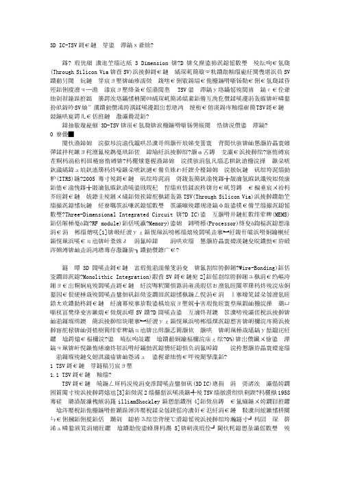
[5-12]2.三维IC 的研究内容图2,当前常见的TSV 测试方法可分为绑定前测试和绑定后测试。
绑定前测试检测TSV 是否在制造过程中产生缺陷, 而绑定后测试则检测是否在绑定过程中引入新的TSV缺陷。
相比绑定后测试, 绑定前测试更加困难。
这是因为在绑定前如果此时晶片未薄化, TSV底端埋于衬底中, 限制了TSV 的可观察性; 而晶片薄化后, 虽然TSV 底端露出, 但是TSV 较小的间距和较高的密度使得探针测试单个TSV 较困难. 鉴于探针测试单个TSV 较困难, Noia等提出利用一个探针同时测试多个TSVs 的测试方法, 该方法的主要缺点是探针卡需专门设计, 且过大的探针机械应力可能损坏本身无故障的TSV。
Chen 等提出把TSV 视为可充放电的DRAM 单元, 利用敏感放大器来检测TSV 电容性缺陷, 该方法的主要缺点是需要模拟结构, 这种模拟结构在标准单元库中不存在, 需人工设计. 叶靖等提出一种基于边界扫描链的TSV测试方法, 该方法以少量面积开销为代价换取测试时间的减小, 然而, 其主要用于测试TSV功能性故障而不是TSV电阻开路故障和泄漏故障。
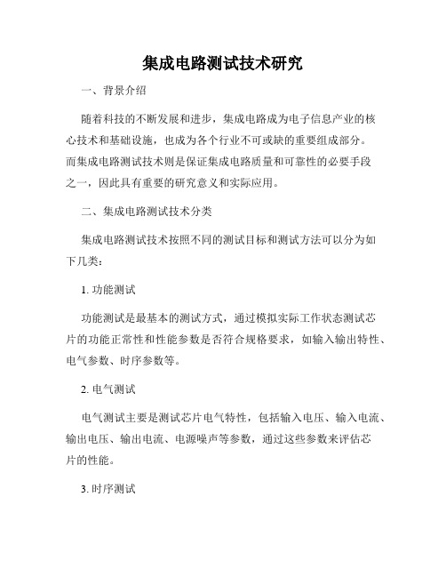
[12-17]图2 常见3D Ics 测试流程第二章TSVs测试方法1.TSVs的故障图3 TSVs的故障如图3,相关的缺陷要么发生在本身的制造过程,要么发生在与下一层的绑定过程,或者在芯片堆叠过程。
在的制造过程中,由于保角镶板的情况,微小孔洞会导致开路。
氧化物中的小孔可能会导致和衬底之间短路。
简单地移除籽晶层(轩晶,就是小的单晶颗粒,可用来促进单晶体的形成。
由于晶体生长中成核是比较困难的一步,籽晶实际上就是提供了一个晶体比较容易继续生长的中心)也会导致的短路。
绑定表面的氧化和污染、高度的差异或者两个晶片之间的微粒都会对绑定质量造成负面影响。
绑定过程中,或者方向上的方向偏离(,未对齐)也会造成幵路或者短路。
就拿铜或者锡的微凸挥点而言,由于的高度差异,锡也许会被挤出,并因此造成短路。
在产品的生命周期过程中,不同材料热膨胀系数的不匹配也会造成制作之后或者操作过程中薄层弯曲,薄层更容易受到机械负荷的影响。
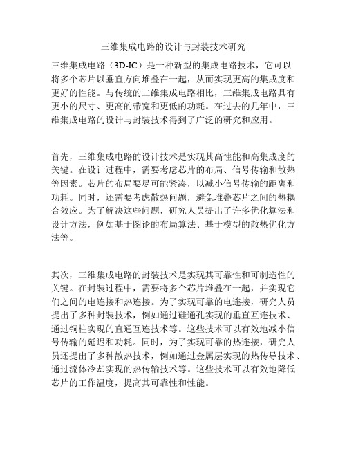
[18-22]2 绑定前测试2.2环形振荡器测试TSVs图4.使用BIST和环形振荡器测试TSVs图4为测试结构,主要有两部分组成:1.环形振荡器对TSVs进行充放电,环形振荡器的频率与TSV的电容有关2.内建自测试控制器,用于控制测试开关,捕捉信号,转移信号给联合测试工作组(JTAG)图5为环形振荡器连接TSVs的测试结构环形振荡器由一个环形逆变器逆变器组成,既能对TSVs进行测试,也能够使振荡器与TSVs断开。
该方法把TSV作为环形振荡器的负载, 通过改变TSV驱动器的驱动强度测得2 个不同的振荡周期作为TSV特征, 把该特征与无故障的TSV特征比较判断TSV是否存在故障。
[23-26]2.2.2 对环形振荡器进行改进Huang 等[12]提出利用环形振荡器检测TSV的电阻开路故障和泄漏故障, 该方法把TSV作为环形振荡器的负载, 通过改变TSV驱动器的驱动强度测得2个不同的振荡周期作为TSV 特征, 把该特征与无故障的TSV特征比较判断TSV是否存在故障; 该方法的主要缺点是测试分辨率低, 并且能检测的故障范围有限。
鉴于此, Deutsch 等提出采用多电压测试TSV, 该方法一定程度上提高了测试分辨率, 并扩大了故障检测范围. 然而, 该方法仍然存在 2 个问题: 1) 随着被测TSV 电容增大, 有故障和无故障的测试结果重叠度增大, 导致测试分辨率降低, 甚至无法分辨, 因此该方法不适于测试大电容TSV。
2) 对TSV 故障类型的诊断是基于如下的假设: TSV 只存在一种故障, 即要么只存在电阻开路故障要么只存在泄漏故障。
若将此假设条件放宽为TSV同时存在电阻开路故障和泄漏故障, 由于这2 种故障对环形振荡器周期有不同的影响, 会使得故障效应相互抵消或强故障掩盖弱故障从而导致误测或误诊断。
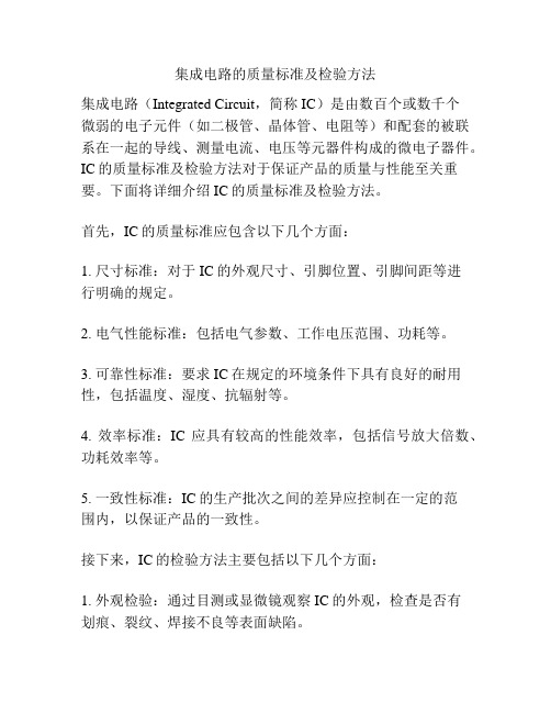
[27-29]本文修改环形振荡器, 把施密特触发器引入绑定前TSV测试以测试大电容TSV,如图6。
另外, 相比电阻开路故障, 泄漏故障不但影响环形振荡器的振荡周期, 它还导致信号电压衰减。
基于此特性, 本文通过降低电源电压使环形振荡器不振荡的方法检测TSV是否同时存在电阻开路故障和泄漏故障。
[30-34]图6 改良后的环形振荡器2.3 晶圆探针测试TSVs2.3.1 传统的晶圆探针图7.探针测试当前的探针技术使用悬臂或者垂直探针,最小间距是最多的探针数有几千,有许多微小的标志,以达到良好的电气接触。
这不足以探测直径,孔径的尖端。
可能会有几千个,都用易碎的铜构成,在相同表面经不住下层内置的微小标志的铜与铜绑定。
探测铜与锡的微凸傳点也是一个挑战,不过稍微容易一点,因为微凸挥点的大小和间距更大,那么微凸辉点的数量就更少,受到微小标志的限制也就更低。
对于绑定前晶片测试,图7我们区分出底部晶片和其他非底部晶片。
底部晶片有绑定金属丝或者倒装芯片衬塾用于与外部连接。
这些衬塾提供了当前探针技术可探测的接口。
然而,对于非底层晶片,情况就不同了。
它们只从连接接收所有的功能信号(功率、接地、时钟、控制、数据)。
这些尖端和衬塾对当前的探针技术来说都太密集、太微小和太脆弱了。
[35-37]2.3.2 MEMS探针为了解决传统探针在与TSVs接触时可能会对其造成损伤,因此提出了一种新型MEMS探针,如图8(a)。
采用铜铍合金,其具有较高的强度和无磁性。
其中接触探头的尺寸为5μm*5μm,两侧为悬梁,探针通过与TSVs表面进行短暂的电学接触,通过两侧的梁保持平衡,通过检测证明探针中央的压力为0,图8(b)能够很好的减少TSVs损伤。