CXK77B3611AGB-中文资料
ducky one说明书

ducky one说明书作为来自宝岛台湾的著名外设品牌Ducky,自从2022年创立,已经陪伴海内外用户走过了十一个年头。
早期凭借出色的制造工艺和优秀的设计,以“魔力鸭”、“AKKODucky”之名在大陆也获得了众多玩家的喜爱,zero系列,以及One系列,生肖限定系列等都是大家耳熟能详的产品。
不过,在2022年6月19日,Ducky正式结束与前代理商AKKO的合作,取“DUCKY,DUCKY!LUCKY,LUCKY!”之有趣含义,宣布更名为“吉利鸭”,由Ducky总部独立运营大陆市场。
为了感谢前代理AKKO的工作,Ducky也将zero 3系列(含3108、3087、3068、3084等)友情出让给AKKO品牌,从此与台湾创杰国际公司旗下品牌Ducky吉利鸭不再有任何关联。
近日,由Ducky总部独立运营的吉利鸭就在大陆发售了全新的主题键盘,Ducky One2“冲鸭”主题。
外设天下也在近期收到了这款键盘,接下来就由笔者为大家带来这款键盘的评测吧。
Ducky One2“冲鸭”主题机械键盘外包装采用了硬纸质包装,包装的设计风格依旧延续了之前One2外包装设计方案,红、蓝、黄三色ONE字母构成的立方体,在包装上还是十分显眼的。
左上角Ducky的LOGO与右侧ONE 2字符均采用烫金工艺制作,反光下淡淡的紫色更增加了外观辨识度。
包装背面则附有常规的产品尺寸、生产地址等信息。
掀开包装上盖,可以看到键盘被透明塑料材质完全包裹,内包装填充也十分牢固,能够有效避免键盘在物流过程中出现磨损、擦伤等情况。
在附件方面,Ducky吉利鸭也保持了一贯的水准,透明键盘防尘罩、替换键帽、拔键器、键盘连接线、说明书与质保卡,附件内容十分的丰富。
键盘底壳整体设计十分简单,但又不失层次感,四角设计有四枚长条状的防滑脚垫,来确保键盘放置使用时的稳固性。
它还采用了键线分离设计,中置出线口,并提供了三向理线槽,方便用户根据不同的桌面布局来调整走线方式。
AKG K-77 监听耳机

AKG K-77 监听耳机
品牌: 爱科技AKG 型号: K-77
K77作为新一代全封闭监听耳机,佩带更舒适,设计更人性,特别是在整个录音中,耳机对低音方面的灵敏度更高,这就便于歌手或者乐手在演奏中能够听清楚低鼓,从而保证了节奏的准确性。
从这一点看来,K77的价格应该是很合理的。
这个耳机可以自动调节频率响应,耳机的阻抗或者外部的压力等,以便歌手乐手获得最大的舒适度。
技术参数:
类型:全封闭的, 动圈式耳机
灵敏度:115 dB/V
频率响应:18 to 20,000 Hz
阻抗: 32 Ω
最大输入功率: 200 mW
附带: 2.5 米长的耳机线材
标准耳机接口,带有专业的大三芯转接头
耳机重量:(不带线 190 g )
总体运输重量(带包装): 400 g。
MP3内芯你懂吗

MP3内芯你懂吗?主流解码芯片详解MP3内芯你懂吗?主流解码芯片详解点击此处查看全部新闻图片如今购买MP3,理性的消费者一般不只关注外观以及功能,最主要还是机器本身的品质。
MP3的解码芯片已经为越来越多的消费者所关注,不过市场中几千款MP3,到底有哪些解码芯片为其提供良好的品质呢?那就请关注以下这篇文章吧!一、飞利浦芯片产地:荷兰如果一定要评出目前市场上最好的MP3解码芯片的话,那么无疑就是飞利浦芯片了。
飞利浦家族的解码芯片在业界一直以其“功能全,音质好,价格高”而著称。
飞利浦的解码芯片一般都采用的是BGA封装工艺,而国内的这方面技术相当有限,此外,由于飞利浦的解码芯片需要搭配另外的控制芯片电路协同工作,所以产品成本较高。
所以采用飞利浦解码芯片的厂商往往都定位于中高价位,如MPIO和IRIVER这两家韩国的MP3专业厂商。
这两个品牌一个最主要的共同特点就是在产品中全面采用了飞利浦的解码芯片。
因此,他们的产品拥有很高的音质和品质,成为全球MP3爱好者追逐的对象。
1、飞利浦SAA775X系列(SAA7750/7751/7752/7753)飞利浦SAA775x芯片是目前市场上MP3播放器解码芯片组中功能最全(支持CD直录),效果最好的解码芯片之一。
该解码芯片的音质表现为:低音下沉较深、中音表现出色、而相比之下高音则显得一般。
MP3内芯你懂吗?主流解码芯片详解点击此处查看全部新闻图片因为SAA775x中内含DSP(Digital Signal Processing,数字信号处理)和32位ARM RISC处理器,所以能用超高集成度的单颗芯片,音频解码和语音编码等工作,并且可以加入SDMI(Secure Digital Music Initiative,安全式数字音乐)保护其中SAA7750内含DSP和32位ARM RISC处理器,信噪比为90dB。
该芯片兼容多段多档位EQ智能音效,支持以AD PC M格式保存语音记录、同步显示歌名和歌曲信息、Line-in直录,此外还支持USB 1。
CXD2951GA-2资料

ARM7TDMI
RTC
Timer 3ch
RAM 72KB
ROM 288KB
I/O UART A/D
Compared with conventional methods, position detection time and sensitivity are substantially improved with the use of an advanced signal processing scheme. With the integration of both the Radio and baseband blocks into a single CMOS IC, the CXD2951GA-2 is ideal for use in automotive, cellular handset, handheld navigation, mobile computing and other location-based applications.
1575.42MHz LNA
TCXO CPU
Freq. Synthesizer
RF/IF 1575.42MHz → 1.023MHz
BPF
SAW
TCXO Reference clock
18.414MHz (GPS, Sony standard)
Down Converter
LPF 1 bit
LNA
1.023MHz
• PLL spurious (typ.): –45dBc (inside fosc ±1.023MHz) –55dBc (outside fosc ±1.023MHz)
Note) These values are not guaranteed.
HT77XX中文资料

HT77XXPFM Step-up DC/DC ConverterSelection TablePart No.Output VoltagePackageMarkingHT7727 2.7V TO-92SOT-89SOT-25HT77XX (for TO-92)HT77XX#(for SOT-89)77XX#(for SOT-25)HT7730 3.0V HT7733 3.3V HT7737 3.7V HT77505.0VNote:²XX ²stands for output voltages.Only lead free devices are available.²#²stands for lead free devices.For the TO-92package,there will be a ²#²mark at the end of the date code.Rev 1.101March 7,2006Features·Low start-up voltage:0.6V (Typ.)·High efficiency:85%(Typ.)·High output voltage accuracy:±2.5%·Output voltage:2.7V,3.0V,3.3V,3.7V,5.0V·Ultra low supply current I DD2:4m A (Typ.)·Low ripple and low noise·Low shutdown current:0.5m A (Typ.)·TO-92,SOT-89and SOT-25packageApplications·Palmtops/PDAs·Portable communicators/Smartphones·Cameras/Camcorders ·Battery-powered equipmentGeneral DescriptionThe HT77XX series is a set of PFM step-up DC/DC con-verter with high efficiency and low ripple.The series fea-tures extremely low start-up voltage and high output voltage accuracy.They require only three external com-ponents to provide a fixed output voltage of 2.7V,3.0V,3.3V,3.7V or 5.0V.CMOS technology ensures ultra low supply current and makes them ideal for bat-tery-operated applications powered from one or more cells.The HT77XX consists of an oscillator,a PFM control cir-cuit,a driver transistor,a reference voltage unit,and a high speed comparator.They employ pulse frequency modulation (PFM)for minimum supply current and rip-ple at light output loading.These devices are available in space saving TO-92,SOT-89and SOT-25packages.For SOT-25package,it also build-in a chip enable func-tion to reducepower consumption during shutdown mode.Technical Document·Tools Information ·FAQs·Application NoteBlock DiagramPin AssignmentPin DescriptionPin No.Pin Name DescriptionTO-92SOT-25SOT-89¾1¾CE Chip enable pin,high active222VOUT DC/DC converter output monitoring pin¾3¾NC No connection141GND Ground pin353LX Switching pinAbsolute Maximum RatingsSupply Voltage..............................V SS-0.3V to V SS+7V Storage Temperature............................-50°C to125°C Power Consumption(*1)..................................500mW Operating Temperature...............................0°C to70°C Power Consumption(*2)..................................250mWNote:These are stress ratings only.Stresses exceeding the range specified under²Absolute Maximum Ratings²may cause substantial damage to the device.Functional operation of this device at other conditions beyond those listed in the specification is not implied and prolonged exposure to extreme conditions may affect device reliabil-ity.*1:applied to SOT-89and TO-92*2:applied to SOT-25Rev1.102March7,2006Electrical CharacteristicsHT7727,+2.7V Output Type V IN =V OUT ´0.6;I OUT =10mA;Ta=25°C (Unless otherwise specified)Symbol ParameterTest ConditionsMin.Typ.Max.Unit V OUT Output Voltage ¾ 2.633 2.7 2.767V V IN Input Voltage ¾¾¾6V V START Start-up VoltageV IN :0®2V;I OUT =1mA ¾0.60.7V V HOLD Minimum Hold-on Voltage V IN :2®0V;I OUT =1mA ¾¾0.7V I IN No load Input Current Measured at no load ¾10¾m A I DD1Supply Current 1V IN =V OUT ´0.95Measured at VOUT pin ¾40¾m A I DD2Supply Current 2V IN =V OUT +0.5VMeasured at VOUT pin ¾47m A I SHDN Shutdown Current V CE =V IL ,V IN =V OUT ´0.95¾0.5¾m A I LEAK LX Leakage CurrentV IN =6V¾¾0.9m A f OSC Maximum Oscillator Frequency V IN =V OUT ´0.95Measured at LX pin¾115¾kHz h Efficiency¾¾85¾%D OSCOscillator Duty CycleV IN =V OUT ´0.95Measured at LX pin657585%HT7730,+3.0V Output Type V IN =V OUT ´0.6;I OUT =10mA;Ta=25°C (Unless otherwise specified)Symbol ParameterTest ConditionsMin.Typ.Max.Unit V OUT Output Voltage ¾ 2.9253 3.075V V IN Input Voltage ¾¾¾6V V START Start-up Voltage V IN :0®2V;I OUT =1mA ¾0.60.7V V HOLD Min.Hold-on Voltage V IN :2®0V;I OUT =1mA ¾¾0.7V I IN No load Input Current Measured at no load ¾10¾m A I DD1Supply Current 1V IN =V OUT ´0.95Measured at VOUT pin ¾48¾m A I DD2Supply Current 2V IN =V OUT +0.5VMeasured at VOUT pin ¾47m A I SHDN Shutdown Current V CE =V IL ,V IN =V OUT ´0.95¾0.5¾m A I LEAK LX Leakage CurrentV IN =6V¾¾0.9m A f OSC Maximum Oscillator Frequency V IN =V OUT ´0.95Measured at LX pin¾115¾kHz h Efficiency¾¾85¾%D OSCOscillator Duty CycleV IN =V OUT ´0.95Measured at LX pin657585%Rev 1.103March 7,2006Symbol ParameterTest ConditionsMin.Typ.Max.Unit V OUT Output Voltage ¾ 3.218 3.3 3.382V V IN Input Voltage ¾¾¾6V V START Start-up Voltage V IN :0®2V;I OUT =1mA ¾0.60.7V V HOLD Min.Hold-on Voltage V IN :2®0V;I OUT =1mA ¾¾0.7V I IN No load Input Current Measured at no load ¾10¾m A I DD1Supply Current 1V IN =V OUT ´0.95Measured at VOUT pin ¾60¾m A I DD2Supply Current 2V IN =V OUT +0.5VMeasured at VOUT pin ¾47m A I SHDN Shutdown Current V CE =V IL ,V IN =V OUT ´0.95¾0.5¾m A I LEAK LX Leakage CurrentV IN =6V¾¾0.9m A f OSC Maximum Oscillator Frequency V IN =V OUT ´0.95Measured at LX pin¾115¾kHz h Efficiency¾¾85¾%D OSCOscillator Duty CycleV IN =V OUT ´0.95Measured at LX pin657585%HT7737,+3.7V Output Type V IN =V OUT ´0.6;I OUT =10mA;Ta=25°C (Unless otherwise specified)Symbol ParameterTest ConditionsMin.Typ.Max.Unit V OUT Output Voltage ¾ 3.608 3.7 3.793V V IN Input Voltage ¾¾¾6V V START Start-up Voltage V IN :0®2V;I OUT =1mA ¾0.60.7V V HOLD Min.Hold-on Voltage V IN :2®0V;I OUT =1mA ¾¾0.7V I IN No load Input Current Measured at no load ¾10¾m A I DD1Supply Current 1V IN =V OUT ´0.95Measured at VOUT pin ¾64¾m A I DD2Supply Current 2V IN =V OUT +0.5VMeasured at VOUT pin ¾47m A I SHDN Shutdown Current V CE =V IL ,V IN =V OUT ´0.95¾0.5¾m A I LEAK LX Leakage CurrentV IN =6V¾¾0.9m A f OSC Maximum Oscillator Frequency V IN =V OUT ´0.95Measured at LX pin¾115¾kHz h Efficiency¾¾85¾%D OSCOscillator Duty CycleV IN =V OUT ´0.95Measured at LX pin657585%Rev 1.104March 7,2006Symbol ParameterTest ConditionsMin.Typ.Max.Unit V OUT Output Voltage ¾ 4.8755 5.125V V IN Input Voltage ¾¾¾6V V START Start-up Voltage V IN :0®2V;I OUT =1mA ¾0.70.8V V HOLD Min.Hold-on Voltage V IN :2®0V;I OUT =1mA ¾¾0.7V I IN Current Consumption Measured at no load ¾10¾m A I DD1Supply Current 1V IN =V OUT ´0.95Measured at VOUT pin ¾85¾m A I DD2Supply Current 2V IN =V OUT +0.5VMeasured at VOUT pin ¾47m A I SHDN Shutdown Current V CE =V IL ,V IN =V OUT ´0.95¾0.5¾m A I LEAK LX Leakage CurrentV IN =6V¾¾0.9m A f OSC Maximum Oscillator Frequency V IN =V OUT ´0.95Measured at LX pin¾115¾kHz h Efficiency¾¾85¾%D OSCOscillator Duty CycleV IN =V OUT ´0.95Measured at LX pin657585%Typical Performance CharacteristicsL=220m H,C=47m FHT7730Efficiency vs.Output CurrentRev 1.105March 7,2006L=220m H,C=47m FHT7730Output Voltage vs.Output CurrentL=220m H,C=47m FHT7730Maximum Oscillator Frequency vs.TemperatureRev1.106March7,2006Application CircuitsNote:For the SOT-25package,when CE is pulled low,the internal blocks of the device,such as the reference band gap,gain block,and all feedback and control circuitry will be switched off.The boost converter¢s output,VOUT, will be at a value one Schottky diode voltage drop below the input voltage and the LX pin remains in a high im-pedance condition.The output capacitor and load at VOUT determine the rate at which VOUT decays.Rev1.107March7,2006Package Information3-pin TO-92Outline DimensionsSymbolDimensions in milMin.Nom.Max.A170¾200B170¾200C500¾¾D11¾20E90¾110F45¾55G45¾65H130¾160I8¾18a4°¾6°Rev1.108March7,2006SymbolDimensions in milMin.Nom.Max.A173¾181B64¾72C90¾102D35¾47E155¾167F14¾19G17¾22H¾59¾I55¾63J14¾17Rev1.109March7,2006SymbolDimensions in mmMin.Nom.Max.A 1.00¾ 1.30A1¾¾0.10A20.70¾0.90b0.35¾0.50C0.10¾0.25D 2.70¾ 3.10E 1.40¾ 1.80e¾ 1.90¾H 2.60¾3L0.37¾¾q1°¾9°Rev1.1010March7,2006Product Tape and Reel SpecificationsTO-92Reel Dimensions(Unit:mm)Rev1.1011March7,2006SOT-89&SOT-25Reel DimensionsSOT-89Symbol Description Dimensions in mmA Reel Outer Diameter180±1.0B Reel Inner Diameter62±1.5C Spindle Hole Diameter12.75+0.15D Key Slit Width 1.9±0.15T1Space Between Flange12.4+0.2T2Reel Thickness17-0.4SOT-25Symbol Description Dimensions in mmA Reel Outer Diameter178±1.0B Reel Inner Diameter62±1.0C Spindle Hole Diameter13.0±0.2D Key Slit Width 2.5±0.25T1Space Between Flange 8.4+1.5-0.0T2Reel Thickness11.4+1.5Rev1.1012March7,2006TO-92Carrier Tape DimensionsTO-92Symbol Description Dimensions in mm I1Taped Lead Length(2.5)P Component Pitch12.7±1.0P0Perforation Pitch12.7±0.3P2Component to Perforation(Length Direction) 6.35±0.4F1Lead Spread 2.5+0.4-0.1F2Lead Spread 2.5+0.4-0.1D h Component Alignment0±0.1W Carrier Tape Width 18.0+1.0-0.5W0Hold-down Tape Width 6.0±0.5W1Perforation Position9.0±0.5W2Hold-down Tape Position(0.5)H0Lead Clinch Height16.0±0.5H1Component Height Less than24.7D0Perforation Diameter 4.0±0.2t Taped Lead Thickness0.7±0.2H Component Base Height19.0±0.5Note:Thickness less than0.38±0.05mm~0.5mmP0Accumulated pitch tolerance:±1mm/20pitches.()Bracketed figures are for reference only.Rev1.1013March7,2006SOT-89&SOT-25Carrier Tape DimensionsSOT-89Symbol Description Dimensions in mmW Carrier Tape Width 12.0+0.3-0.1P Cavity Pitch8.0±0.1E Perforation Position 1.75±0.1F Cavity to Perforation(Width Direction) 5.5±0.05D Perforation Diameter 1.5+0.1D1Cavity Hole Diameter 1.5+0.1P0Perforation Pitch 4.0±0.1P1Cavity to Perforation(Length Direction) 2.0±0.10A0Cavity Length 4.8±0.1B0Cavity Width 4.5±0.1K0Cavity Depth 1.8±0.1t Carrier Tape Thickness0.30±0.013C Cover Tape Width9.3SOT-25Symbol Description Dimensions in mm W Carrier Tape Width8.0±0.3P Cavity Pitch 4.0E Perforation Position 1.75F Cavity to Perforation(Width Direction) 3.5±0.05D Perforation Diameter 1.5+0.1D1Cavity Hole Diameter 1.5+0.1P0Perforation Pitch 4.0P1Cavity to Perforation(Length Direction) 2.0A0Cavity Length 3.15B0Cavity Width 3.2K0Cavity Depth 1.4t Carrier Tape Thickness0.20±0.03C Cover Tape Width 5.3Rev1.1014March7,2006Holtek Semiconductor Inc.(Headquarters)No.3,Creation Rd.II,Science Park,Hsinchu,TaiwanTel:886-3-563-1999Fax:886-3-563-1189Holtek Semiconductor Inc.(Taipei Sales Office)4F-2,No.3-2,YuanQu St.,Nankang Software Park,Taipei115,TaiwanTel:886-2-2655-7070Fax:886-2-2655-7373Fax:886-2-2655-7383(International sales hotline)Holtek Semiconductor Inc.(Shanghai Sales Office)7th Floor,Building2,No.889,Yi Shan Rd.,Shanghai,China200233Tel:021-6485-5560Fax:021-6485-0313Holtek Semiconductor Inc.(Shenzhen Sales Office)43F,SEG Plaza,Shen Nan Zhong Road,Shenzhen,China518031Tel:0755-8346-5589Fax:0755-8346-5590ISDN:0755-8346-5591Holtek Semiconductor Inc.(Beijing Sales Office)Suite1721,Jinyu Tower,A129West Xuan Wu Men Street,Xicheng District,Beijing,China100031Tel:010-6641-0030,6641-7751,6641-7752Fax:010-6641-0125Holmate Semiconductor,Inc.(North America Sales Office)46712Fremont Blvd.,Fremont,CA94538Tel:510-252-9880Fax:510-252-9885CopyrightÓ2006by HOLTEK SEMICONDUCTOR INC.The information appearing in this Data Sheet is believed to be accurate at the time of publication.However,Holtek as-sumes no responsibility arising from the use of the specifications described.The applications mentioned herein are used solely for the purpose of illustration and Holtek makes no warranty or representation that such applications will be suitable without further modification,nor recommends the use of its products for application that may present a risk to human life due to malfunction or otherwise.Holtek¢s products are not authorized for use as critical components in life support devices or systems.Holtek reserves the right to alter its products without prior notification.For the most up-to-date information, please visit our web site at .Rev1.1015March7,2006。
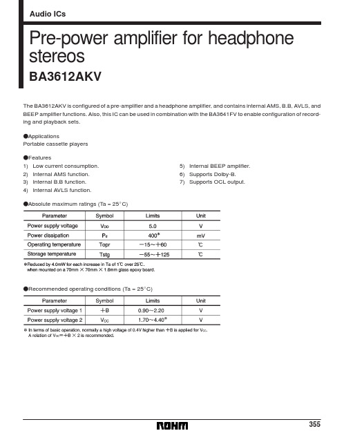
BA3612AKV资料
366
元器件交易网 Audio ICs
FMeasurement circuit
BA3612AKV
367
元器件交易网 Audio ICs
FElectrical characteristic curves
BA3612AKV
FExternal dimensions (Units: m
BA3612AKV
(unless otherwise noted, )B = 1.3V, VCC = 2.3V, f = 1kHz, PreOutRL = 5kΩ, PWROutRL = 16Ω (OCL), Ta = 25_C, and measurement condition pertaining to ripple: VCC and )B are common-mode input)
FBlock diagram
BA3612AKV
356
元器件交易网 Audio ICs
BA3612AKV
FPin descriptions (The pin voltage of VCC = 2.3V, )B = 1.3V is the standard value for the measurement circuit under quiescent conditions. Modes: PWR-ON, TC, FWD, NOR, Mute-OFF, B.B-OFF, AVLS-OFF)
5) Internal BEEP amplifier. 6) Supports Dolby-B. 7) Supports OCL output.
FRecommended operating conditions (Ta = 25_C)
355
雷蛇毒鳍银鲛

Razer Chimaera毒鳍银鲛™ 5.1 Xbox360专用无线游戏耳麦提供逼真的环绕声体验。
此款无线耳麦汇聚了我们在PC游戏中累积的广泛游戏音频专业知识,可提供精确的赛事级5.1定位音频,而其超大罩耳式耳罩可提供极致舒适感。
基站可同时用作充电座和音频处理单元,让您可以调整游戏声效并最多连接四个基站,以便在畅爽无延迟本地交流通道中与队友交谈。
高级用户指南目录1. 包装内物品2. 系统和硬件要求3. 主要特性4. 技术规格5. 安装和设置/注册/安装6. 使用Razer Chimaera毒鳍银鲛5.17. 法律声明1. 包装内物品-适用于 Xbox 360® 的Razer Chimaera毒鳍银鲛 5.1无线游戏耳麦-充电底座基站-线缆:∙光纤∙RCA线缆∙交流电适配器∙ 2.5 毫米至 2.5 毫米立体声线缆(用于控制器连接)∙ 3.5 毫米至 3.5 毫米立体声线缆(用于本地团队通讯)- 2 节 AAA 可充电电池-快速入门指南-高级用户指南2. 系统和硬件要求- Xbox 360®-复合线缆(或分量高清晰 AV 线缆)或者- PC3. 主要特性A. 5.1 环绕声B. 左按键1 –增大麦克风音量C. 左按键 2 –降低麦克风音量D. 右按键 1 –增大音量E. 右按键 2 –降低音量F. 左按键 3 –麦克风静音G. 左按键 4 –电源按键H. 右按键 3 –模式按键(Xbox LIVE/本地团队通讯切换)I. 右按键 4 –音量静音 /同步按键J. 充电 LEDK. 均衡器 LEDL. 杜比耳机 LEDM. 模式(Xbox LIVE/本地团队通讯)LED N. 待机 LEDO. 均衡器/杜比耳机按键P. 待机按键Q. 源/同步按键R. 数字音频输入S. 数字音频输出T. 3.5 毫米输入U. 3.5 毫米输出V. RCA 输入(右侧)W. RCA 输入(左侧)X. 交流电接口4. 技术规格无线耳麦尺寸(毫米): 200 (宽) x 204 (高) x 88 (深)耳机•无线电频率:5.8GHz• Dolby® Headphone / Dolby® Pro Logic® I I / Dolby® Digital •无线范围:33英尺/10米•频响范围:20 - 20,000 Hz•阻抗:32Ω(1kHz时)•灵敏度(@1kHz、1V/Pa时):105dB +/- 2dB•驱动程序:50毫米钕磁铁•电池:2节AAA电池(长达8小时电池使用寿命)•充电时间:3小时麦克风•频响:130 - 10,000 Hz•灵敏度(@1kHz、1V/Pa时):-42 +/- 2dB •信噪比:>55 dB•拾音器模式:单向5. 安装和设置/注册/安装电池安装为了使效果最佳,第一次使用Razer Chimaera 5.1毒鳍银鲛时请将电池完全充满。
LBC847BWT1G

132LBC846AWT1G,BWT1GLBC847AWT1G,BWT1GCWT1GLBC848AWT1G,BWT1GCWT1GSOT–323 /SC–701.FR–5=1.0x 0.75 x 0.062inORDERING INFORMATION General Purpose TransistorsNPN SiliconPb Free–()Device Package Shipping LBC846AWT1G_S SC-703000/Tape&Reel 10000/Tape&ReelLBC846AWT3G_S SC-70We declare that the material of product compliance with RoHS requirements.LBC846AWT1G,BWT1G, LBC847AWT1G,BWT1G, CWT1G, LBC848AWT1G,BWT1G,CWT1GELECTRICAL CHARACTERISTICS (T A = 25°C unless otherwise noted) (Continued)CharacteristicSymbolMinTypMaxUnitON CHARACTERISTICSDC Current Gainh FE(I C = 2.0 mA, V CE = 5.0 V)110180220200290450 420520800Collector–Emitter Saturation Voltage (I C = 10 mA, I B = 0.5 mA)V CE(sat)——0.25V (I C = 100 mA, I B = 5.0 mA)——0.6Base–Emitter Saturation Voltage (I C = 10 mA, I B = 0.5 mA)VBE(sat)—0.7—V (I C = 100 mA, I B = 5.0 mA) —0.9—Base–Emitter Voltage (I C = 2.0 mA, V CE = 5.0 V)V BE(on)580660700mV(I C = 10 mA, V CE = 5.0 V)——770SMALL–SIGNAL CHARACTERISTICSCurrent–Gain — Bandwidth Product f T 100——MHz (I C = 10 mA, V CE = 5.0 Vdc, f = 100 MHz)Output Capacitance (V CB = 10 V, f = 1.0 MHz)C obo —— 4.5pF Noise Figure (I C = 0.2 mA, NF dBV CE = 5.0 V dc , R S = 2.0 k Ω, ——10f = 1.0 kHz, BW = 200 Hz) ——4.0I C , COLLECTOR CURRENT (mAdc)Figure 1. Normalized DC Current GainI C , COLLECTOR CURRENT (mAdc)Figure 2. “Saturation” and “On” Voltages0.20.51.02.05.0102050100200V CE = 10 V T A = 25°C2.01.51.00.80.60.40.30.20.10.20.30.50.7 1.02.03.05.07.01020305070100T A = 25°CV BE(sat) @ I C /I B =10V BE(on) @ V CE = 10 VV CE(sat) @ I C /I B = 10T A = 25°CV , V O L T A G E (V O L T S )1.00.90.80.70.60.50.40.30.20.10θV B , T E M P E R A T U R E C O E F F I C I E N T (m V / °C )1.01.21.62.02.42.8I B , BASE CURRENT (mA)Figure 3. Collector Saturation Region V C E , C O L L E C T O R – E M I T T E R V O L T A G E (V )I C = 200 mA–55°C to +125°CI C , COLLECTOR CURRENT (mA)Figure 4. Base–Emitter Temperature Coefficient2.01.61.20.80.40I C =10 mA I C = 100 mAI C =20 mAI C = 50 mAh F E , N O R M A L I Z E D D C C U R R E N T G A I N0.2 1.0101000.020.11.01020LBC846A, LBC847A, LBC848ALBC846B, LBC847B, LBC848B LBC847C, LBC848C LBC846A, LBC847A,L BC848ALBC846B, LBC847B,L BC848B LBC847C, LBC848CLBC847/LBC848V R , REVERSE VOLTAGE (VOLTS)Figure 5. CapacitancesI C , COLLECTOR CURRENT (mAdc)Figure 6. Current–Gain – Bandwidth ProductI C , COLLECTOR CURRENT (mA)Figure 7. DC Current GainI C , COLLECTOR CURRENT (mA)Figure 8. “On” VoltageI B , BASE CURRENT (mA)Figure 9. Collector Saturation RegionI C , COLLECTOR CURRENT (mA)Figure 10. Base–Emitter Temperature CoefficientT A = 25°CV BE(sat) @ I C /I B = 10V BE @ V CE = 5.0 VV CE = 10V T A = 25°CT A = 25°CV CE = 5V T A = 25°CV CE(sat) @ I C /I B = 10V C E , C O L L E C T O R – E M I T T E R V O L T A G E (V O L T S )θV B , T E M P E R A T U R E C O E F F I C I E N T (m V /°C )h F E , D C C U R R E N T G A I N (N O R M A L I Z E D )V , V O L T A G E (V O L T S )f T , C U R R E N T – G A I N – B A N D W I D T H P R O D U C T (M H z )V , V O L T A G E (V O L T S )I C =10 mA100mA20mA200mAT A = 25°Cθ VB for V BE–55°C to 125°CC obC ib–1.0–1.4–1.8–2.2–2.6–3.01.00.80.60.40.2400300200100806040302010.07.05.03.02.01.02.01.00.50.22.01.61.20.80.400.40.60.81.02.0 4.0 6.08.01020400.50.71.02.03.05.07.0102030500.10.21.0101000.20.5 1.0 2.0 5.01020501002000.20.51.02.05.01020501002000.020.050.10.20.5 1.0 2.0 5.0102050mALBC846AWT1G,BWT1G, LBC847AWT1G,BWT1G, CWT1G, LBC848AWT1G,BWT1G,CWT1GLBC846V R , REVERSE VOLTAGE (VOLTS)Figure 11. CapacitanceI C , COLLECTOR CURRENT (mA)Figure 12. Current–Gain – Bandwidth ProductC , C A P A C I T A N C E (p F )f T , C U R R E N T – G A I N – B A N D W I D T H P R O D U C T TC obC ibT A = 25°CV CE = 5 V T A = 25°C0.10.20.5 1.0 2.0 5.01020501001.0 5.010501004020106.04.02.05002001005020LBC846AWT1G,BWT1G, LBC847AWT1G,BWT1G, CWT1G, LBC848AWT1G,BWT1G,CWT1G3.COLLECTORNOTES:1.DIMENSION I NG AND TOLERANCING PER ANSI Y14.5M, 1982.2.CONTROLLING DIMENSION: INCH.SC -70 / SOT -323LBC846AWT1G,BWT1G, LBC847AWT1G,BWT1G, CWT1G, LBC848AWT1G,BWT1G,CWT1G。
- 1、下载文档前请自行甄别文档内容的完整性,平台不提供额外的编辑、内容补充、找答案等附加服务。
- 2、"仅部分预览"的文档,不可在线预览部分如存在完整性等问题,可反馈申请退款(可完整预览的文档不适用该条件!)。
- 3、如文档侵犯您的权益,请联系客服反馈,我们会尽快为您处理(人工客服工作时间:9:00-18:30)。
Description
The CXK77B3611AGB-5/6 is a high speed 1M bit Bi-CMOS synchronous static RAM organized as 32768 words by 36 bits. This SRAM integrates input registers, high speed SRAM and write buffer onto a single monolithic IC and features the delayed write system to reduce the dead cycles.
Features
•Fast cycle time (Cycle)(Frequency)CXK77B3611AGB-55ns 200MHz
-66ns 167MHz
•Inputs and outputs are GTL/HSTL compatible •Controlled Impedance Driver
•Single 3.3V power supply: 3.3V±0.15V •Byte-write possible •OE asynchronization •JTAG test circuit •Package 119TBGA
•4 kinds of synchronous operation mode Register-Register mode (R-R mode)Register-Flow Thru mode (R-F mode)Register-Latch mode (R-L mode)Dual clock mode (D-C mode)
Function
32768 word x 36bit High Speed Bi-CMOS Synchronous SRAM Structure
Silicon gate Bi-CMOS IC
– 1–
CXK77B3611AGB -5/6
119 pin BGA (Plastic)
PE96812
High Speed Bi-CMOS Synchronous Static RAM
Sony reserves the right to change products and specifications without prior notice. This information does not convey any license by any implication or otherwise under any patents or other right. Application circuits shown, if any, are typical examples illustrating the operation of the devices. Sony cannot assume responsibility for any problems arising out of the use of these circuits.
Preliminary
For the availability of this product, please contact the sales office.
CXK77B3611AGB Block Diagram
DQ
– 2–
– 3–
CXK77B3611AGB
Pin Configuration (Top View)
V DD Q NC NC DQc DQc V DD Q DQc DQc V DD Q DQd DQd V DD Q DQd DQd NC NC V DD Q
A B C D E F G H J K L M N P R T U
A NC A DQc DQc DQc DQc DQc V DD DQd DQd DQd DQd DQd A NC TMS
A NC A V SS V SS V SS BWc V SS VREF V SS BWd V SS V SS V SS M1A TDI
NC NC V DD ZQ S G C C V DD K K W A A V DD A TCK
A NC A V SS V SS V SS BWb V SS VREF V SS BWa V SS V SS V SS M2A TDO
A NC A DQb DQb DQb DQb DQb V DD DQa DQa DQa DQa DQa A NC NC
V DD Q NC NC DQb DQb V DD Q DQb DQb V DD Q DQa DQa V DD Q DQa DQa NC ZZ V DD Q
1
234567Pin Description A DQx K K C C VREF
W
Address Input Data I/O in byte (a to d)Positive Clock Negative Clock
Output Positive Clock(∗)Output Negative Clock(∗)Input Reference
Write Enable BWX S G ZZ
TCK TMS TDI
TDO Byte Write Enable (a to d)Chip Select Asyn Output Enable Sleep Mode Select JTAG Clock JTAG Mode Select JTAG Data In
JTAG Data Out V DD V DD Q V SS M1, M2ZQ NC
+3.3V power supply Output power supply Ground Mode Select Output Impedance Control No Connect
Symbol Description Symbol Description Symbol Description () These pins should be tied to V DD or V SS except D-C mode.
CXK77B3611AGB Package Outline Unit: mm
SONY CODE EIAJ CODE JEDEC CODE
PACKAGE STRUCTURE
PACKAGE MATERIAL
BOARD MATERIAL
TERMINAL MATERIAL
PACKAGE WEIGHT
EPOXY RESIN
COPPER-CLAD LAMINATE
SOLDER
0.8g
119 TERMINAL BGA (PLASTIC)
BGA-119P-01
DETAIL X
– 4–。