基于单片机的多功能温度检测系统的设计翻译
基于单片机的多功能温度检测系统的设计翻译
基于单片机的多功能温度检测系统的设计一、引言随着社会的发展和技术的进步,人们越来越注重温度检测与显示的重要性。
温度检测与状态显示技术与设备已经普遍应用于各行各业,市场上的产品层出不穷。
温度检测及显示也逐渐采用自动化控制技术来实现监控。
本课题就是一个温度检测及状态显示的监控系统。
二、系统方案本系统采用AT89S52 作为该系统的单片机。
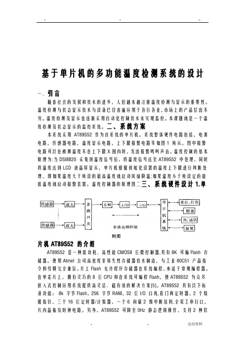
系统整体硬件电路包括,电源电路,传感器电路,温度显示电路,上下限报警电路等如图1 所示。
图中报警电路可以在被测温度不在上下限X围内时,发出报警鸣叫声音。
温度控制的基本原理为:当DSl8B20 采集到温度信号后,将温度信号送至AT89S52 中处理,同时将温度送到LCD 液晶屏显示,单片机根据初始化设置的温度上下限进行判断处理,即如果温度大于所设的最高温度就启动风扇降温;如果温度小于所设定的最低温度就启动报警装置。
温度控制器的原理图二三、系统硬件设计1.单片机AT89S52 的介绍AT89S52 是一种低功耗、高性能CMOS8 位微控制器,具有8K 可编Flash 存储器。
使用Atmel 公司高密度非易失性存储器技术制造,与工业80C51 产品指令和引脚完全兼容。
片上Flash 允许程序存储器在系统编程,亦适于常规编程器。
在单芯片上,拥有灵巧的8 位CPU和在系统可编程Flash,使AT89S52 为众多嵌入式控制应用系统提供高灵活、超有效的解决方案[5]。
AT89S52 具有以下标准功能:8k 字节Flash,256 字节RAM,32 位I/O 口线,看门狗定时器,2 个数据指针,三个16 位定时器/计数器,一个6 向量2 级中断结构,全双工串行口,片内晶振及时钟电路。
另外,AT89S52 可降至0Hz 静态逻辑操作,支持2 种软件可选择节电模式。
空闲模式下,CPU 停止工作,允许RAM、定时器/计数器、串口、中断继续工作。
掉电保护方式下,RAM 内容被保存,振荡器被冻结,单片机一切工作停止,直到下一个中断或硬件复位为止。
基于单片机的实时温度监控系统设计外文翻译毕业设计论文

安徽建筑工业学院毕业设计 (论文)专业电气工程及其自动化班级 07电气(1)课题基于单片机的实时温度监控系统设计基于单片机的实时温度监控系统设计摘要本文所介绍的是一种采用单总线数字式的温度传感器DS18B20与AT89S52单片机组成的新型温度测量系统,并使用LED数码管显示器将所测温度显示出来。
该系统以 AT89S52单片机为控制核心,利用新型一线制温度传感器 DS18B20测量温度值,实现环境温度的检测和报警。
系统测温范围为-40℃—+85℃,测量精度为 0.5℃。
用户可以自定义报警上、下限,一旦温度超过极限值,单片机便启动声光报警系统。
该系统精度高、测温范围广、报警及时,可广泛应用于基于单片机的温报警场合。
关键词:AT89S52单片机;温度测量;DS18B20;声光报警;数码管显示Design of Real-time Temperature Monitoring System Based on Single Chip MicrocomputerAbstractDescribed in this paper is a single-bus digital temperature sensor DS18B20 AT89S52 single chip with a new temperature measuring system,and use the LED digital display will display the measured temperature. The AT89S52 microcontroller for the control system to the core,Temperature sensor system using a new first-line temperature measurement DS18B20,achieve environmental temperature detection and alarm. Temperature measurement range is -40 ℃ - +85 ℃, measurement ac curacy of 0.5 ℃. Users can customize the alarm, the lower limit,Once the temperature exceeds the limit, the microcontroller will start the sound and light alarm system. The system of high precision, wide temperature range, the alarm in time, can be widely used in microcontroller-based temperature alarm occasions.Key words: AT89S52 microcontroller; temperature measurement; DS18B20; sound and light alarms; digital display目录摘要 (2)Abstract (3)目录 (4)第一章前言 (5)第二章监控系统主要元器件简介 (6)2.1 AT89S52单片机的组成结构及功能 (6)2.1 .1 AT89S52单片机的主要功能 (6)2.1.2 AT89S5单片机的封装及其引脚功能说明 (7)2.1.3外接晶振或外部振荡器引脚 (9)2.1.4 AT89S52复位 (9)2.2温度测量传感器DS18B20介绍 (10)2.2.1 DS18B20简介 (10)2.2.2 DS18B20的引脚、封装和结构 (10)2.2.3 寄生电源 (12)2.2.4 温度测量原理 (12)2.3 四位连体数码管SM410564 (13)第三章系统硬件电路设计 (15)3.1 单片机最小系统 (15)3.2 温度检测模块 (17)3.3 温度显示模块电路 (17)3.4报警电路模块 (17)3.5 基于AT89S52单片机的温度测量系统总电路 (18)3.6 温度测量系统的实物图 (19)第四章控制系统软件设计 (21)4.1 主程序 (21)4.2 子程序 (22)4.2.1读出温度子程序 (22)4.2.2温度转换命令子程序 (22)4.2.3计算温度子程序 (23)4.2.4显示数据刷新子程序 (24)第五章结论 (25)参考文献 (26)致谢 (27)附录一英文文献 (28)附录二中文翻译 (37)第一章前言温度是一种最基本的环境参数,对于我们来说,不仅仅是一个量的反映,更能直接影响作用到我们的生活中,人民的生活与环境的温度息息相关,在工业生产过程中需要实时测量温度,在农业生产中也离不开温度的测量。
基于单片机的温度检测与控制器的设计外文翻译 (1)
VTP ,所有的检测放大器晶体管(M1,M2,M3和M4)都偏向于饱和模式。
M1和M3(M2和M4)的栅源电压几乎是相同的,因为相同的电流流过每一个分支。
当PASE 变低时,左右位线具有相同的电位,21V V +。
由于位线电压相同,位线负载(CELL L I I +)和电容(BL I )的电流也相等。
由于存储单元细胞获取电流{CELL I ),成数量的电流(CELL I )在右边流动,以保持位线电压是相等的。
因此,目前DL 和DL 线之间出现了差异。
位线负载电容的传感速度几乎是独立的,因为BL 和BL 没有电容放电操作。
因此,BL 和BL 不需要预充电和均衡操作,从而导致速度和周期时间的损失。
图10.39所示电路的开环增益表示为 )2(*)1()4(*)3(m gm m gm m gm m gm Gain loop open =-gm(m1),gm(m2),gm(m3)和gm(m4)是M1,M2,M3和M4,分别。
电流检测放大器的一个缺点是大于电压检测放大器的功耗。
“这些放大器通常用于在高速SRAM 和高密度比如由于数据线的大负载电容256 MB DRAM (IO BL _和IOB BL _如图.10.15)。
14.4 非易失性存储器如DRAM 和SRAM 的MOS 内存结构的缺点是,在没有电源的情况下导致的数据丢失。
为了克服这个问题,各种非易失性和可编程(除掩模ROM )内存已提出。
最近,快闪记忆体的基础上浮动门的概念已成为最流行的非易失性存储器,由于其小单元尺寸和更好的功能。
因此,我们将详细描述的基本结构和操作掩模ROM 和在本节中的快闪记忆体。
只读存储器阵列,也可以被看作是一个简单的组合的布尔网络为每个输入组合,即产生一个指定的输出值,每个地址。
因此,存储在一个特定的地址位置的二进制信息可实现了从选定行(字线)选定的列(位线),这是等价的存在或缺乏设备在特定的位置。
在下面,我们将研究两个不同实现的MOS ROM 的阵列。
基于单片机的实时温度监控系统设计外文翻译毕业设计论文

毕业设计 (论文)专业电气工程及其自动化班级 07电气(1)基于单片机的实时温度监控系统设计摘要本文所介绍的是一种采用单总线数字式的温度传感器DS18B20与AT89S52单片机组成的新型温度测量系统,并使用LED数码管显示器将所测温度显示出来。
该系统以AT89S52单片机为控制核心,利用新型一线制温度传感器DS18B20测量温度值,实现环境温度的检测和报警。
系统测温范围为-40℃—+85℃,测量精度为0.5℃。
用户可以自定义报警上、下限,一旦温度超过极限值,单片机便启动声光报警系统。
该系统精度高、测温范围广、报警及时,可广泛应用于基于单片机的温报警场合。
关键词:AT89S52单片机;温度测量;DS18B20;声光报警;数码管显示Design of Real-time Temperature Monitoring System Based on Single Chip MicrocomputerAbstractDescribed in this paper is a single-bus digital temperature sensor DS18B20 AT89S52 single chip with a new temperature measuring system,and use the LED digital display will display the measured temperature. The AT89S52 microcontroller for the control system to the core,Temperature sensor system using a new first-line temperature measurement DS18B20,achieve environmental temperature detection and alarm. Temperature measurement range is -40 ℃- +85 ℃, measurement accuracy of 0.5 ℃. Users can customize the alarm, the lower limit,Once the temperature exceeds the limit, the microcontroller will start the sound and light alarm system. The system of high precision, wide temperature range, the alarm in time, can be widely used in microcontroller-based temperature alarm occasions.Key words: AT89S52 microcontroller; temperature measurement; DS18B20; sound and light alarms; digital display目录摘要 (2)Abstract (3)目录 (4)第一章前言 (5)第二章监控系统主要元器件简介 (6)2.1 AT89S52单片机的组成结构及功能 (6)2.1 .1 AT89S52单片机的主要功能 (6)2.1.2 AT89S5单片机的封装及其引脚功能说明 (7)2.1.3外接晶振或外部振荡器引脚 (9)2.1.4 AT89S52复位 (9)2.2温度测量传感器DS18B20介绍 (10)2.2.1 DS18B20简介 (10)2.2.2 DS18B20的引脚、封装和结构 (10)2.2.3 寄生电源 (12)2.2.4 温度测量原理 (12)2.3四位连体数码管SM410564 (13)第三章系统硬件电路设计 (15)3.1 单片机最小系统 (15)3.2 温度检测模块 (17)3.3 温度显示模块电路 (17)3.4报警电路模块 (17)3.5 基于AT89S52单片机的温度测量系统总电路 (18)3.6 温度测量系统的实物图 (19)第四章控制系统软件设计 (21)4.1 主程序 (21)4.2 子程序 (22)4.2.1读出温度子程序 (22)4.2.2温度转换命令子程序 (22)4.2.3计算温度子程序 (23)4.2.4显示数据刷新子程序 (24)第五章结论 (25)参考文献 (26)致谢 (27)附录一英文文献 (28)附录二中文翻译 (37)第一章前言温度是一种最基本的环境参数,对于我们来说,不仅仅是一个量的反映,更能直接影响作用到我们的生活中,人民的生活与环境的温度息息相关,在工业生产过程中需要实时测量温度,在农业生产中也离不开温度的测量。
单片机温度控制系统中英文翻译资料
中文4243字英文原文DescriptionThe at89s52 is a low-power, high-performance CMOS 8-bit microcomputer with 4K bytes of Flash Programmable and Erasable Read Only Memory (PEROM) and 128 bytes RAM. The device is manufactured using Atmel’s high density nonvolatile me mory technology and is compatible with the industry standard MCS-51™ instruction set and pinout. The chip combines a versatile 8-bit CPU with Flash on a monolithic chip, the Atmelat89s52 is a powerful microcomputer which provides a highly flexible and cost effective solution to many embedded control applications.Features:• Compatible with MCS-51™ Products• 4K Bytes of In-System Reprogrammable Flash Memory• Endurance: 1,000 Write/Erase Cycles• Fully Static Operation: 0 Hz to 24 MHz• Three-Level Program Memory Lock• 128 x 8-Bit Internal RAM• 32 Programmable I/O Lines• Two 16-Bit Timer/Counters• Six Interrupt Sources• Programmable Serial Channel• Low Power Idle and Power Down ModesThe at89s52 provides the following standard features: 4K bytes of Flash, 128 bytes of RAM, 32 I/O lines, two 16-bit timer/counters, a five vectortwo-level interrupt architecture, a full duplex serial port, on-chip oscillator and clock circuitry. In addition, the at89s52 is designed with static logic for operation down to zero frequency and supports two software selectable power saving modes. The Idle Mode stops the CPU while allowing the RAM, timer/counters, serial port and interrupt system to continue functioning. The Power Down Mode saves the RAM contents but freezes the oscillator disabling all other chip functions until the next hardware reset.Pin Description:VCC Supply voltage.GND Ground.Port 0Port 0 is an 8-bit open drain bidirectional I/O port. As an output port each pin can sink eight TTL inputs. When is are written to port 0 pins, the pins can be used as high impedance inputs.Port 0 may also be configured to be the multiplexed loworderaddress/data bus during accesses to external program and data memory. In this mode P0 has internal pullups.Port 0 also receives the code bytes during Flash programming, and outputs the code bytes during program verification. External pullups are required during program verification.Port 1Port 1 is an 8-bit bidirectional I/O port with internal pullups. The Port 1 output buffers can sink/source four TTL inputs. When 1s are written to Port 1 pins they are pulled high by the internal pullups and can be used as inputs. As inputs, Port 1 pins that are externally being pulled low will source current (IIL) because of the internal pullups.Port 1 also receives the low-order address bytes during Flash programming and verification.Port 2Port 2 is an 8-bit bidirectional I/O port with internal pullups. The Port 2 output buffers can sink/source four TTL inputs. When 1s are written to Port 2 pins they are pulled high by the internal pullups and can be used as inputs. As inputs, Port 2 pins that are externally being pulled low will source current (IIL) because of the internal pullups.Port 2 emits the high-order address byte during fetches from external program memory and during accesses to external data memory that use 16-bit addresses (MOVX @ DPTR). In this application it uses strong internalpull-ups when emitting 1s. During accesses to external data memory that use 8-bit addresses (MOVX @ RI), Port 2 emits the contents of the P2 Special Function Register.Port 2 also receives the high-order address bits and some control signals during Flash programming and verification.Port 3Port 3 is an 8-bit bidirectional I/O port with internal pullups. The Port 3 output buffers can sink/source four TTL inputs. When 1s are written to Port 3 pins they are pulled high by the internal pullups and can be used as inputs. As inputs, Port 3 pins that are externally being pulled low will source current (IIL) because of the pullups.Port 3 also serves the functions of various special features of theat89s52 as listed below:Port 3 also receives some control signals for Flash programming andverification.RSTReset input. A high on this pin for two machine cycles while theoscillator is running resets the device.ALE/PROGAddress Latch Enable output pulse for latching the low byte of the address during accesses to external memory. This pin is also the program pulse input (PROG) during Flash programming.In normal operation ALE is emitted at a constant rate of 1/6 theoscillator frequency, and may be used for external timing or clockingpurposes. Note, however, that one ALE pulse is skipped during each access to external Data Memory.If desired, ALE operation can be disabled by setting bit 0 of SFRlocation 8EH. With the bit set, ALE is active only during a MOVX or MOVC instruction. Otherwise, the pin is weakly pulled high. Setting the ALE-disable bit has no effect if the microcontroller is in external execution mode.PSENProgram Store Enable is the read strobe to external program memory. When the at89s52 is executing code from external program memory, PSEN is activated twice each machine cycle, except that two PSEN activations are skipped during each access to external data memory.EA/VPPExternal Access Enable. EA must be strapped to GND in order to enable the device to fetch code from external program memory locations starting at 0000H up to FFFFH. Note, however, that if lock bit 1 is programmed, EA will be internally latched on reset. Port pinalternate functions P3.0rxd (serial input port) P3.1txd (serial output port) P3.2^int0 (external interrupt0) P3.3^int1 (external interrupt1) P3.4t0 (timer0 external input) P3.5t1 (timer1 external input) P3.6^WR (external data memory write strobe) P3.7 ^rd (external data memory read strobe)EA should be strapped to VCC for internal program executions.This pin also receives the 12-volt programming enable voltage(VPP) during Flash programming, for parts that require 12-volt VPP.XTAL1Input to the inverting oscillator amplifier and input to the internal clock operating circuit.XTAL2Output from the inverting oscillator amplifier.Oscillator CharacteristicsXTAL1 and XTAL2 are the input and output, respectively, of an inverting amplifier which can be configured for use as an on-chip oscillator, as shown in Figure 1. Either a quartz crystal or ceramic resonator may be used. To drive the device from an external clock source, XTAL2 should be left unconnected while XTAL1 is driven as shown in Figure 2. There are no requirements on the duty cycle of the external clock signal, since the input to the internal clocking circuitry is through a divide-by-two flip-flop, but minimum and maximum voltage high and low time specifications must be observed.Idle ModeIn idle mode, the CPU puts itself to sleep while all the onchip peripherals remain active. The mode is invoked by software. The content of the on-chip RAM and all the special functions registers remain unchanged during this mode. The idle mode can be terminated by any enabled interrupt or by a hardware reset.It should be noted that when idle is terminated by a hard ware reset, the device normally resumes program execution, from where it left off, up to two machine cycles before the internal reset algorithm takes control. On-chip hardware inhibits access to internal RAM in this event, but access to the port pins is not inhibited. To eliminate the possibility of an unexpected write to a port pin when Idle is terminated by reset, the instruction following the one that invokes Idle should not be one that writes to a port pin or to external memory.Status of External Pins During Idle and Power Down Modesmode Program memory ALE ^psen Port0 Port1Port2Port3idle internal 1 1 data data data Data Idle External 1 1 float Data data Data Power down Internal 0 0 Data Data Data Data Power down External 0 0 float data Data data Power Down ModeIn the power down mode the oscillator is stopped, and the instructionthat invokes power down is the last instruction executed. The on-chip RAMand Special Function Registers retain their values until the power down modeis terminated. The only exit from power down is a hardware reset. Resetredefines the SFRs but does not change the on-chip RAM. The reset shouldnot be activated before VCC is restored to its normal operating level andmust be held active long enough to allow the oscillator to restart andstabilize.Program Memory Lock BitsOn the chip are three lock bits which can be left unprogrammed (U) orcan be programmed (P) to obtain the additional features listed in the tablebelow:Lock Bit Protection ModesWhen lock bit 1 is programmed, the logic level at the EA pin issampled and latched during reset. If the device is powered up without a reset,the latch initializes to a random value, and holds that value until reset isactivated. It is necessary that the latched value of EA be in agreement with the current logic level at that pin in order for the device to function properly. Programming the Flash:The at89s52 is normally shipped with the on-chip Flash memory array in the erased state (that is, contents = FFH) and ready to be programmed.The programming interface accepts either a high-voltage (12-volt) or alow-voltage (VCC) program enable signal.The low voltage programming mode provides a convenient way to program the at89s52 inside the user’s system, while the high-voltage programming mode is compatible with conventional third party Flash or EPROM programmers.The at89s52 is shipped with either the high-voltage or low-voltage programming mode enabled. The respective top-side marking and device signature codes are listed in the following table.Vpp=12v Vpp=5vTop-side mark at89s52xxxxyywwat89s52xxxx-5yywwsignature (030H)=1EH(031H)=51H(032H)=FFH (030H)=1EH (031H)=51H (032H)=05HThe at89s52 code memory array is programmed byte-bybyte in either programming mode. To program any nonblank byte in the on-chip Flash Programmable and Erasable Read Only Memory, the entire memory must be erased using the Chip Erase Mode.Programming Algorithm:Before programming the at89s52, the address, data and control signals should be set up according to the Flash programming mode table and Figures 3 and 4. To program the at89s52, take the following steps.1. Input the desired memory location on the address lines.2. Input the appropriate data byte on the data lines.3. Activate the correct combination of control signals.4. Raise EA/VPP to 12V for the high-voltage programming mode.5. Pulse ALE/PROG once to program a byte in the Flash array or the lock bits. The byte-write cycle is self-timed and typically takes no more than 1.5 ms. Repeat steps 1 through 5, changing the address and data for the entire array or until the end of the object file is reached.Data Polling: The at89s52 features Data Polling to indicate the end of a write cycle. During a write cycle, an attempted read of the last byte written will result in the complement of the written datum on PO.7. Once the write cycle has been completed, true data are valid on all outputs, and the next cycle may begin. Data Polling may begin any time after a write cycle has been initiated.Ready/Busy: The progress of byte programming can also be monitored by the RDY/BSY output signal. P3.4 is pulled low after ALE goes high during programming to indicate BUSY. P3.4 is pulled high again when programming is done to indicate READY.Program Verify: If lock bits LB1 and LB2 have not been programmed, the programmed code data can be read back via the address and data lines for verification. The lock bits cannot be verified directly. Verification of the lock bits is achieved by observing that their features are enabled.Chip Erase: T he entire Flash Programmable and Erasable Read Only Memory array is erased electrically by using the proper combination of control signals and by holding ALE/PROG low for 10 ms. The code array is written with all “1”s. The chip erase operation must be executed before the code memory can be re-programmed.Reading the Signature Bytes: The signature bytes are read by the same procedure as a normal verification of locations 030H, 031H, and 032H, except that P3.6 and P3.7 must be pulled to a logic low. The values returned are as follows.(030H) = 1EH indicates manufactured by Atmel(031H) = 51H indicates 89C51(032H) = FFH indicates 12V programming(032H) = 05H indicates 5V programmingProgramming InterfaceEvery code byte in the Flash array can be written and the entire array can be erased by using the appropriate combination of control signals. The write operation cycle is selftimed and once initiated, will automatically time itself to completion.中文翻译描述at89s52是美国ATMEL公司生产的低电压,高性能CMOS8位单片机,片内含4Kbytes的快速可擦写的只读程序存储器(PEROM)和128 bytes 的随机存取数据存储器(RAM),器件采用ATMEL公司的高密度、非易失性存储技术生产,兼容标准MCS-51产品指令系统,片内置通用8位中央处理器(CPU)和flish存储单元,功能强大at89s52单片机可为您提供许多高性价比的应用场合,可灵活应用于各种控制领域。
(完整word版)单片机_温度控制系统_外文翻译_外文文献_英文文献_中英翻译

Design of the Temperature Control System Based on AT89C51ABSTRACTThe principle and functions of the temperature control system based on micro controller AT89C51 are studied, and the temperature measurement unit consists of the 1-Wire bus digital temperature sensor DS18B20。
The system can be expected to detect the preset temperature,display time and save monitoring data. An alarm will be given by system if the temperature exceeds the upper and lower limit value of the temperature which can be set discretionarily and then automatic control is achieved, thus the temperature is achieved monitoring intelligently within a certain range。
Basing on principle of the system, it is easy to make a variety of other non-linear control systems so long as the software design is reasonably changed。
The system has been proved to be accurate,reliable and satisfied through field practice. KEYWORDS: AT89C51; micro controller; DS18B20;temperature1 INTRODUCTIONTemperature is a very important parameter in human life。
单片机温度探测系统中英文对照外文翻译文献

中英文对照翻译附件1:外文资料翻译译文一种基于DS18B20的温度探测系统摘要所有的DS18B20传感器,用于多点温度测试,IO总线与MCU连接,温度数据的轮流收集。
如果系统有大量的传感器,MCU的时间用在处理温度数据明显延长,因此周期替代测试变得更长。
在本文中,一种新的方法,DS18B20的合理组合和一些在软件上采取的措施,替代试验进展速度明显。
关键词:DS18B20的集团,温度测试,轮流测试所花费的时间。
引言由于结构简单,安装方便,低损失和广泛的用途的温度测试,DS18B20温度测试传感器应用领域,需要多点温度测试,如化学工业,粮食,环境监督管理等。
因为通过一个DS18B20的多点温度测试系统总线,所有DS18B20是挂在一条总线上,然后每个温度测试点的值转换轮流读。
作为转换后读值必须阅读8次引脚的状态,移动时间,位置和存储数据,所以时间多花费在阅读每一个点的数据系统时间。
如果温度测试系统是大型系统由它造成的损失是相当多的,然后交替测试系统的运行速度明显降低,从而影响多点温度测试系统的效率。
在本文中,DS18B20的一些I / O总线上都挂着分组DS18B20的均匀,温度转换获取数据读取DS18B20的状态,系统损耗减少和替代测试速度增加显然,这将不会影响精度和转换的可靠性。
一套点对多点温度,在此实现人工环境实验室测试,这增加了测试效率。
作者对DS18B20的认识DS18B20是单总线数字温度传感器来自美国达拉斯公司。
DS18B20是由64数字光盘刻激光,温度敏感性组成部分,非易失性温度报警触发器(设备TH和TL)。
DS18B20的通信微处理器单总线端口和测试范围DS18B20是从-55摄氏度到+125摄氏度,增量值是0.5摄氏度。
温度可在720ms的数字改为每个DS18B20具有唯一的64数字序号。
图1揭示的具体内容:两个8的数字储量(0号和1号),用于存储在DS18B20的温度值。
0号存储存储器温度值,补充和一号存储器温度值的符号。
单片机-温度控制系统-外文翻译-外文文献-英文文献-中英翻译
Design of the Temperature Control System Based on AT89C51ABSTRACTThe principle and functions of the temperature control system based on micro controller AT89C51 are studied, and the temperature measurement unit consists of the 1-Wire bus digital temperature sensor DS18B20. The system can be expected to detect the preset temperature,display time and save monitoring data. An alarm will be given by system if the temperature exceeds the upper and lower limit value of the temperature which can be set discretionarily and then automatic control is achieved, thus the temperature is achieved monitoring intelligently within a certain range. Basing on principle of the system, it is easy to make a variety of other non—linear control systems so long as the software design is reasonably changed。
The system has been proved to be accurate, reliable and satisfied through field practice. KEYWORDS: AT89C51; micro controller; DS18B20;temperature1 INTRODUCTIONTemperature is a very important parameter in human life. In the modern society, temperature control (TC) is not only used in industrial production, but also widely used in other fields. With the improvement of the life quality,we can find the TC appliance in hotels, factories and home as well. And the trend that TC will better serve the whole society,so it is of great significance to measure and control the temperature。
- 1、下载文档前请自行甄别文档内容的完整性,平台不提供额外的编辑、内容补充、找答案等附加服务。
- 2、"仅部分预览"的文档,不可在线预览部分如存在完整性等问题,可反馈申请退款(可完整预览的文档不适用该条件!)。
- 3、如文档侵犯您的权益,请联系客服反馈,我们会尽快为您处理(人工客服工作时间:9:00-18:30)。
基于单片机的多功能温度检测系统的设计一、引言随着社会的发展和技术的进步,人们越来越注重温度检测与显示的重要性。
温度检测与状态显示技术与设备已经普遍应用于各行各业,市场上的产品层出不穷。
温度检测及显示也逐渐采用自动化控制技术来实现监控。
本课题就是一个温度检测及状态显示的监控系统。
二、系统方案本系统采用 AT89S52 作为该系统的单片机。
系统整体硬件电路包括,电源电路,传感器电路,温度显示电路,上下限报警电路等如图1 所示。
图中报警电路可以在被测温度不在上下限范围内时,发出报警鸣叫声音。
温度控制的基本原理为:当DSl8B20 采集到温度信号后,将温度信号送至AT89S52 中处理,同时将温度送到LCD 液晶屏显示,单片机根据初始化设置的温度上下限进行判断处理,即如果温度大于所设的最高温度就启动风扇降温;如果温度小于所设定的最低温度就启动报警装置。
温度控制器的原理图三、系统硬件设计1.单片机AT89S52 的介绍AT89S52 是一种低功耗、高性能CMOS8 位微控制器,具有8K 可编Flash 存储器。
使用Atmel 公司高密度非易失性存储器技术制造,与工业80C51 产品指令和引脚完全兼容。
片上Flash 允许程序存储器在系统编程,亦适于常规编程器。
在单芯片上,拥有灵巧的8 位CPU和在系统可编程Flash,使AT89S52 为众多嵌入式控制应用系统提供高灵活、超有效的解决方案[5]。
AT89S52 具有以下标准功能: 8k 字节Flash,256 字节RAM,32 位I/O 口线,看门狗定时器,2 个数据指针,三个16 位定时器/计数器,一个6 向量2 级中断结构,全双工串行口,片内晶振及时钟电路。
另外,AT89S52 可降至0Hz 静态逻辑操作,支持2 种软件可选择节电模式。
空闲模式下,CPU 停止工作,允许RAM、定时器/计数器、串口、中断继续工作。
掉电保护方式下,RAM 内容被保存,振荡器被冻结,单片机一切工作停止,直到下一个中断或硬件复位为止。
2.DS18B20 传感器的介绍在传统的模拟信号远距离温度测量系统中,需要很好的解决引线误差补偿问题、多点测量切换误差问题和放大电路零点漂移误差问题等技术问题,才能够达到较高的测量精度。
另外一般监控现场的电磁环境都非常恶劣,各种干扰信号较强,模拟温度信号容易受到干扰而产生测量误差,影响测量精度[5]。
因此,在温度测量系统中,采用抗干扰能力强的新型数字温度传感器是解决这些问题的最有效方案,与其它温度传感器相比DSl820 具有以下特点:(1)独特的单线接口方式。
DSl820 在与微处理器连接时仅需要一条接口线即可实现微处理器与DSl820 的双向通讯。
(2)多点功能简化了分布式温度检测的应用。
(3)DSl820 在使用中无需任何外围元件。
(4)可用数据线供电,电压范围从3.0V 到5.5V。
(5)可测量的温度范围从-55℃到+125℃,增量值0. 5℃;华氏温度范围从-67 到+257,增量值0.9。
(6)支持多点组网功能。
多个DS1820 可以并接在同一条总线上,实现多点测温。
(7)9 位的温度分辨率。
测量结果以9 位数字量方式串行传送。
(8)用户可设定温度报警门限值。
(9)有超温度搜寻功能。
(1) DSl8B20 的工作原理DS18B20 的内部结构DSl8B20 的测温原理框图如图3.2 所示。
图中低温度系数品振的振荡频率受温度影响很小,用于产生同定频率的脉冲信号送给计数器l。
高温度系数晶振随温度变化其振荡频率明显改变。
所产生的信号作为计数器2 的脉冲输入。
计数器1、计数器2 和温度寄存器被预置在-55℃所对应的一个基数值。
计数器l 对低温度系数晶振产生的脉冲信号进行减法计数,当计数器1 的预置值减到O 时,温度计数器的值将加l,计数器l 的预置值将被重新装人,计数器l 重新开始对低温度系数晶振产生的脉冲信号进行计数,如此循环直到计数器2 计数到O 时,停止温度寄存器的累加,此时温度寄存器中的数值即为所测温度。
图3.2 中的斜率累加器用于补偿和修正测温过程中的非线性,其输出小于修正计数器l 的预置值。
(2) DS18B20 与AT89S52 的接口方式DS18B20 与单片机的连接方式有两种:即寄生电源方式和外部电源方式。
寄生电源方式:在寄生电源供电方式下,DS18B20 从单线信号线上汲取能量:在信号线DQ 处于高电平期间把能量储存在内部电容里,在信号线处于低电平期间消耗电容上的电能工作,直到高电平到来再给寄生电源(电容)充电。
寄生电源方式有三个好处: 1)进行远距离测温时,无需本地电源。
2)可以在没有常规电源的条件下读取ROM。
3)电路更加简洁,仅用一根I/O 口实现测温。
要想使DS18B20 进行精确的温度转换,I/O 线必须保证在温度转换期间提供足够的能量,由于每个DS18B20 在温度转换期间工作电流达到1mA,当几个温度传感器挂在同一根I/O 线上进行多点测温时,只靠4.7K 上拉电阻就无法提供足够的能量,会造成无法转换温度或温度误差极大。
外部电源供电方式:在外部电源供电方式下,DS18B20 工作电源由VDD 引脚接入,此时I/O 线不需要强上拉,不存在电源电流不足的问题,可以保证转换精度,同时在总线上理论可以挂接任意多个DS18B20 传感器,组成多点测温系统。
本系统采用外部电源方式。
连接方法即DS18B20 的1 脚接地,2 脚(DQ 引脚)与AT89S52 的一根I/O 口线相连,3 脚接+5V。
在A89S52 的I/O 口线与+5V 之间连接一4.7K 的上拉电阻,以保证数据采集的正常进行。
若要组成多点温度检测系统,可在单片机的同一根I/O 口线上,以相同的连接方法并联多片DS18B20 芯片。
3、LCD1602 液晶屏1602 液晶显示模块可以和单片机AT89S52 直接接口。
4、蜂鸣器驱动电路由于蜂鸣器的工作电流一般比较大,以致于单片机的I/O 口是无法直接驱动的,所以要利用放大电路来驱动,一般使用三极管来放大电流就可以了。
当所测的温度低于6 摄氏度时,报警。
5、风扇电路当所测的温度高于80 摄氏度时,启动风扇电路。
因为工作电流比较大,所以用放大电路来驱动,即用三极管来放大电流就可以了。
当温度高于80℃时,给单片机一个命令,单片机P2.6 引脚输出高电平,三极管导通,风扇电路接通,电风扇开始转动,从而起到降温作用。
四、系统的软件设计本系统采用AT89S52 作为核心处理器件,把经过DSl8B20 现场实时采集到的温度数据,存入AT89S52 的内部数据存储器,送液晶显示,并与预先设定值进行比较,然后由单片机输出信号去控制风扇电路和报警电路。
多功能温度检测显示系统软件主要包括:函数声明、延迟时间函数、DS18B20 初始化函数、读出DS18B20 当前的温度、温度数据转化成液晶字符显示等程序。
五、小结随着工业的不断发展,对温度测量的要求来越高,而且测量范围也越来越广,因此对温度检测技术的要求也越来越高。
本文介绍了以DSl8B20 新型数字温度传感器、AT89S52 单片机、LCD1602 液晶显示模块为主体构建的温度检测显示系统。
说明了系统硬件电路、系统主程序与各模块子程序的设计。
本系统采用的是DALLAS 公司推出的数字式温度传感器DS18B20,无需外加A/D 即可输出数字量,把温度信号直接转换成串行数字信号供微机处理。
因此。
该系统具有硬件电路结构简单、转换精度高、显示结果清晰稳定、成本低等显着优点。
在诸如粮库测温、智能建筑、中央空调等多种需要温度检测的场合具有较好的应用前景。
Based on SCM multi-functional temperature testingsystem design1、prefaceWith the development of society and the technological progress, people pay more and more attention to the importance of temperature detection and display. Temperature detection and status display technology and equipment has been widely applied in industries, products on the market emerge in endlessly. Temperature testing and also gradually adopt the automatic control technology to realize the monitor. This topic is a temperature testing and status of the monitoring system.2、System solutionsThis system USES the monolithic integrated circuit AT89S52 as this system. The whole system, the hardware circuit including power supply circuit, sensor, the temperature display circuit circuit, upper alarm circuit such as shown in figure 1. Figure in the alarming circuit can be measured in upper temperature range, screaming voice alarm. The basic principle for the temperature control DSl8B20: when the temperature signal acquisition to after temperature signal sent to handle, AT89S52 temperature to LCD screen, SCM according to initialize the upper temperature setting, namely, if the judgement of temperature than the highest temperature cooling fan is started, If the temperature is less than the lowest temperature setting on alarm device. Temperature controller diagram3、The system hardware design(1)AT89S52 SCM are introducedAT89S52 devices is a low power consumption, high CMOS8 bit micro-controller, 8K programmable Flash memory. Use Atmel company high-density nonvolatile storage technology, and industrial 80C51 product instruction and pin fully compatible. The Flash memory chips allows programs in system programming, also suitable for conventional programming. In a single chip, have clever 8 bits CPU and programmable Flash in the system, for many embedded control AT89S52 application system provides a highly flexible, efficient solutions [5]. AT89S52 has the following functions: the standard 256 bytes, 8k byte Flash RAM, 32 I/O port, the watchdog timer, 2 data, three pointer 16 timer/counter, a 6 vector level 2 interrupt structure, full-duplex serial, timely clock circuit within crystals. In addition, 0Hz AT89S52 candrop to the static logic operation, support two software can choose power saving mode. Idle mode, the CPU to stop working, and allows the RAM, timer/counters, serial, continue to work. Protection mode, RAM by MCU, oscillator is frozen, all the work to stop until the next interruption or hardware reset.(2)The sensor DS18B20In the traditional analog signal distance temperature measuring system, need good solve lead error compensation, multi-point measurement error and amplifying circuit switching technologies such as zero drift error problem, can achieve high measuring accuracy. Another general monitoring site of the electromagnetic environment is very bad, all kinds of jamming signal is stronger, the simulated temperature signal interference and vulnerable to produce measurement error and measuring precision [5]. Therefore, in temperature measuring system, the strong anti-jamming capability of the new digital temperature sensor is the most effective to solve these problems, compared with other temperature sensor DSl820 has the following features:(1) the unique singleline interface way. DSl820 in connection with the microprocessor only need one interface to implement line DSl820 microprocessors and two-way communication. (2) more function simplifies distributed temperature detection application. (3) DSl820 in use without any peripheral devices. (4) power, voltage range data available from 3.0 V to 5.5 V. (5) can measure temperature range from - 55 degrees c + + to 125, incremental value 0. 5 ° c, Fahrenheit temperature range from - 67 to + 257, incremental value 0.9. (6) support multi-point network function. Multiple DS1820 can pick on the same bus and, more temperature measurement. (7) 9 temperature resolution. Measuring results in nine serial transmission way the digital quantity. (8) user can set temperature alarm threshold. (9) have super temperature search function.①.DSl8B20 principle of workThe internal structure of DS18B20 DSl8B20 temperature measurement principle diagram shown in figure 3.2. Low temperature coefficient graph oscillation frequency vibration product temperature is used to produce with fixed frequency, pulse signal to counter l. High temperature coefficient crystals temperature-dependent its oscillation frequency change significantly. The signal generated as the counter 2 input pulses. Counter 1, 2 and temperature registers are counter in - 55 degrees preset corresponding a base value. Counter l to low temperature coefficient of the pulse signal generated crystals, when the counter for subtraction counting the preset value reduced to 1, when the temperature counter O value will add l, counter the preset value will be l man again, to counter the l start low temperature coefficient of crystal oscillator pulse signal, so cycle count until the counter 2, stop counting to O accumulative temperature, temperature of the register for the register is measured values. Figure 3.2 accumulative used for the slope compensation and fixed temperature measurement, the output of the process of nonlinear correction is less than the preset value counter l.②.AT89S52 interface mode and DS18B20Chip DS18B20 and the connection has two kinds: namely parasitic power and external power supply mode.Parasitic power way: in the parasitic power supply mode, the signal from the single chip DS18B20 in line drawing energy during the high level in the DQ energy stored in the internal capacitance, low level in signal in the energy consumed during the capacitance on working until high-level coming again to parasitic power (battery). Parasitic power mode has three advantages: 1) distance measuring temperature, without the local power supply. 2) no conventional power in the condition reads the ROM. 3) circuit, with only one more concise root I/O realize temperature measurement. Want to make precise temperature conversion chip DS18B20, I/O line must ensure that the temperature conversion period, due to provide enough energy conversion in temperature during each DS18B20, when the current 1mA to work a few temperature sensor in the same root hanging on the I/O multi-point temperature measurement, only by 4.7 K and resistance will not be able to provide enough energy, which cannot be switchover temperature or errors.The external power source supply way: in the external power supply modes, DS18B20 work power by VDD pin, I/O access line does not need strong pull up, there is no shortage of electricity power, can ensure accuracy and conversion in the bus theory can be articulated multiple sensor DS18B20, multipoint temperature measuring system.This system USES the external power source. Connection method is one foot grounding and DS18B20 2 feet (DQ) and AT89S52 foot an I/O port, 3 feet line up + 5V. A89S52 in the I/O port and + 5V connection between a 4.7 K pull-up resistors, to ensure the normal operation of the data collection. If you want to test system, composed multi-point temperature in the same root chip I/O port in the same line, and the method of connecting the parallel more pieces of DS18B20 chip.(3)LCD1602 LCD1602 LCD module can and monolithic integrated circuit AT89S52 directly interface.(4)Buzzer driver circuitDue to the working current buzzer is compared commonly big, so I/O microcontroller is not directly driven by amplifying circuit, so it is generally used to drive, to enlarge current transistor. When the temperature is below six degrees Celsius, alarm.(5)Fan circuitWhen the temperature is higher than 80 ° c, start fan circuit. Because the job is great, so use current amplifier circuit to drive, to enlarge current transistor. When the temperature is above 80 ° c, give a command, P2.6 single-chip microcontroller foot output level, triode conduction, fans, electric circuit, which began to turn it down.4、The design of the software systemThis system USES AT89S52 devices as the core, with DSl8B20 after the collected data, and the temperature inside the data storage AT89S52 deposit, LCD display, and compared with the prior value, and then the output signal by MCU control circuit and alarm circuit fan. Multi-functional temperature testing system software mainly include: function declarations, time delay function and DS18B20 initialization function, read the temperature, temperature DS18B20 data into a liquid crystal display characters such programs.5、SummaryWith the continuous development of industry of temperature measurement, the higher requirement, and more and more wide measuring range, so are the requirements for temperature detection technology more and more is also high.DSl8B20 introduced new digital temperature sensor and AT89S52 SCM, LCD1602 LCD module for constructing the temperature testing system. The hardware circuit and main program and system design of each module subroutines. This system USES the DALLAS is the digital temperature sensor DS18B20, plus A/D can output the digital quantity, the temperature signal directly convert serial digital signal processing for microcomputer. Accordingly. This system has the hardware circuit structure is simple, high precision, and shows the result conversion clear stability, low cost and significant advantages. In temperature measurement, such as grain of intelligent building, central air conditioning of the occasion to temperature testing has good application prospects.。