据传 诺基亚EOS将配有四核处理器
教你如何巧妙利用诺基亚1020的4100万像素

教你如何巧妙利用诺基亚1020的4100万像素随着手机拍照的普及,很多厂商都推出了旗下主打拍照的手机,其中拥有4100万像素诺基亚808 PureView可以说是令人印象深刻。
而继这款拍照机皇之后,诺基亚便推出了旗下首款搭载WP8系统的诺基亚920,这款手机在弱光方面的表现十分突出。
如今,诺基亚推出了一款将高像素和WP8系统完美融合的手机——诺基亚1020,那么这款手机相比之前诺基亚的手机新增了哪些拍照功能呢?今天小编便和大家一起来盘点盘点。
强大的Nokia专业拍摄作为目前诺基亚最高端的拍照手机,诺基亚1020除了采用一枚4100万像素摄像头之外,还内置了Nokia专业拍摄功能,该功能也是针对诺基亚1020独家定制的,它拥有很多非常专业的拍照功能,使用起来非常得心应手。
可自定义快门按键功能相比前作诺基亚925而言,诺基亚1020做了很多升级,主要体现在拍照界面和功能方面。
诺基亚1020长按快门键现在默认启动的是诺基亚专业拍摄了,而不是原生拍照界面,不过这个选项也可以在设置中调节。
左划快门键可调出快捷设置界面可以说,诺基亚1020新增的NOKIA专业拍摄功能是这款手机的核心,正因为有了这个功能,诺基亚1020才拥有区别于一般手机的专业拍摄体验。
NOKIA专业拍摄功能虽然功能强大,但操作起来并不难。
通过向左滑动拍照界面右侧的快门键,即可调出快捷的相机设置界面。
相机设置界面详解我们知道,一般为了方便用户操作,很多手机的拍照界面都尽可能做的简洁明了,当然诺基亚1020也是如此。
所以很多专业功能都隐藏在设置中了,比如取景网格、画面比例、拍照模式以及面部检测等等。
多种构图方式为了方便用户拍照,诺基亚1020在专业拍摄功能中还加入了多种构图方式,它们分别为三分法、黄金比例、十字线、正方形,大家可以根据自己的爱好选择不同的取景网格。
双重拍照方便社交对于个人用户来说,使用手机拍摄照片有很大一部分是为了社交网络使用,不论是QQ还是微博,传播图片信息几乎成为必修课。
诺基亚手机CPU频率一览
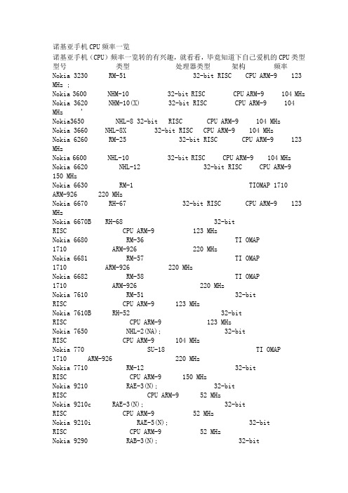
诺基亚手机CPU频率一览诺基亚手机(CPU)频率一览转的有兴趣,就看看,毕竟知道下自己爱机的CPU类型型号类型处理器类型架构频率Nokia 3230 RM-51 32-bit RISC CPU ARM-9 123 MHz ; Nokia 3600 NHM-10 32-bit RISC CPU ARM-9 104 MHz Nokia 3620 NHM-10(X) 32-bit RISC CPU ARM-9 104 MHz ' Nokia3650 NHL-8 32-bit RISC CPU ARM-9 104 MHzNokia 3660 NHL-8X 32-bit RISC CPU ARM-9 104 MHzNokia 6260 RM-25 32-bit RISC CPU ARM-9 123 MHz Nokia 6600 NHL-10 32-bit RISC CPU ARM-9 104 MHz Nokia 6620 NHL-12 32-bit RISC CPU ARM-9 150 MHz Nokia 6630 RM-1 TIOMAP 1710 ARM-926 220 MHzNokia 6670 RH-67 32-bit RISC CPU ARM-9 123 MHz Nokia 6670B RH-68 32-bit RISC CPUARM-9 123 MHzNokia 6680 RM-36 TI OMAP1710 ARM-926 220 MHzNokia 6681 RM-57 TI OMAP1710 ARM-926 220 MHzNokia 6682 RM-58 TI OMAP1710 ARM-926 220 MHzNokia 7610 RM-51 32-bit RISC CPUARM-9 123 MHzNokia 7610B RH-52 32-bit RISC CPUARM-9 123 MHzNokia 7650 NHL-2(NA); 32-bit RISC CPUARM-9 104 MHzNokia 770 SU-18 TI OMAP1710 ARM-926 220 MHzNokia 7710 RM-12 32-bit RISC CPUARM-9 150 MHzNokia 9210 RAE-3(N); 32-bit RISC CPUARM-9 52 MHzNokia 9210c RAE-3(N); 32-bit RISC CPUARM-9 52 MHzNokia 9210i RAE-5(N); 32-bit RISC CPUARM-9 52 MHzNokia 9290 RAB-3(N); 32-bit RISC CPUARM-9 52 MHzNokia 9300 RAE-6(N); TI OMAP 1510 ARM-925 150 MHNokia 9300B RA-4 TI OMAP1510 ARM-925 150 MHz1510 ARM-925 150 MHNokia 9500 RA-2 TI OMAP1510 ARM-925 150 MHzNokia 9500B RA-3 TI OMAP1510 ARM-925 150 MHzNokia E50-1 RM-170 TI OMAP1710 ARM-926 220 MHzNokia E50-2 RM-171 TI OMAP1710 ARM-926 220 MHzNokia E60 RM-49 TI OMAP1710 ARM-926 220 MHzNokia E61 RM-89 TI OMAP1710 ARM-926 220 MHNokia E62-1 RM-8 TI OMAP1710 ARM-926 220 MHzNokia E62-1 RM-8A TI OMAP1710 ARM-926 220 MHzNokia E70-1 RM-10 TI OMAP1710 ARM-926 220 MHzNokia E70-2 RM-24 TI OMAP1710 ARM-926 220 MHzNokia N-Gage NEM-4 32-bit RISCCPU ARM-9 104 MHzNokia N-Gage QD RH-29 32-bit RISC CPU ARM-9 104 MHzNokia N-Gage QDA RH-47 32-bit RISC CPUARM-9 104 MHzNokia N70-1 RM-84 TI OMAP1710 ARM-926 220 MHzNokia N70-5 RM-99 TI OMAP1710 ARM-926 220 MHzNokia N71-1 RM-67 TI OMAP1710 ARM-926 220 MHzNokia N71-5 RM-112 TI OMAP1710 ARM-926 220 MHz ,Nokia N72-5 RM-180 TI OMAP1710 ARM-926 220 MHzNokia N73-1 RM-133 TI OMAP1710 ARM-926 220 MHzNokia N73-? RM-132 TI OMAP1710 ARM-926 220 MHzNokia N80-1 RM-92 TI OMAP1710 ARM-926 220 MHz1710 ARM-926 220 MHzNokia N90-1 RM-42 TI OMAP1710 ARM-926 220 MHzNokia N91-1 RM-43 TI OMAP1710 ARM-926 220 MHzNokia N91-5 RM-158 TI OMAP1710 ARM-926 220 MHzNokia N92 TI OMAP1710 ARM-926 220 MHzNokia N93-1 RM-55 TI OMAP2420 ARM-11 330 MHzNokia N93-5 RM-153 TI OMAP 2420 ARM-11 330 MHz分析NOKIA手机的CPU 让你认清N73,N95,6120c和57006600等机的CPU由于过于古老,在此不讨论从6630开始使用,在现在N73 N70 N72 N71等机用的是ARM9架构的德州仪器OMAP1710 CPU,频率220MHz,以下称为方案一N93 N93i N95 E90等强机使用的是ARM11架构 OMAP2420,频率330MHz,以下称为方案二N76 6610N 5700 6120C 6290等新出的NOKIA机子,使用ARM11架构 Freescale MXC300-30,称为方案三N93 N93i N95 E90等机不是一般能承受得起,在本文,重点讨论方案一和方案三在NOKIA的网站上,我们可以了解到方案一的CPU信息是Dual CPUCPU Type: ARM 9CPU Clock Rate: 220 MHz而方案三是Single CPUCPU Type: ARM 11CPU Clock Rate: 369 MHz关于这两个CPU的争论相当多,尤其是最近N76 5700等新机的速度相当快,得益于高CPU频率,但看了CPU信息后,大家都会产生疑问: 方案一是Dual CPU,方案三是Single CPU,从字面理解就是方案一是双核,方案三是单核,刚公布此消息时,不知其中道理的网友甚至还抱怨怎么换成单核的呢?本来已经够慢了,以后还要更慢? 在官方得到了解释(在GOOGLE找到,由于是E文,这里我给大家大概讲下意思)The"dual-CPU" in the case of N71 means that theres_disibledevent="TEXT-DECORATION: underline"href="/desktop_pc_index/subcate27_list_1.html" ; target=_blank>电脑用的双核CPU 这不像电脑上的双核和单核的关系,OMAP1710CPU,有一个核心运行在220MHz,用于处理手机的用户界面,多媒体应用,JAVA等等之类的应用(这里相当于电脑的CPU的功能),另外一个核心用于处理网络数据(也就是电话功能,打电话,发短信之内的,上网/3G也应该包括,但肯定不处理WIFI数据) 也就是说,OMAP1710是3G时代NOKIA采用的CPU,用此CPU的必有3G版本,以前的旧CPU机是没有3G的这样的好处是无论你运行多大的软件,占用了多少CPU资源,都不会影响到接电话这样的手机最基本功能再来看看 Freescale MXC300-30,方案三,从卖ARM芯片的网站上找到的介绍MXC300-30:3G手机用单核调制解调器处理器,能提供完整UTMS平台的,包括组合了基带和应用处理器,RF,功率放大器和功率管理,高达250MHz的StarCore SC140 DSP,高达532MHz的ARM11应用处理器,四波段GSM850/900/1800/1900MHz,WCDMA三波段850/1900/2100MHz,UTMS数据速率: DL 384Kbps,UL384Kbps,HSDPA 为1.8Mbps(DL),GSM EDGE无线电接入网络(GERAN)数据速率(最大): DL236Kbps,UL 118Kbps,GPRS/EGPRS(EDGE)时隙,高达Class12(4d/4u),最适合的开放式操作系统如Linux和Symbian,不需要增加任何的处理器或加速器,用于GMSK的单天线干扰消除,集成了图像处理单元(IPU)视频加速器,无线连接特性包括支持A-GPS接口,蓝牙接口,以及支持无线LAN 802.11a/b/g接口和DVB-H接口,处理器可用在各种手持设备如MP3播放器,手持DVD播放器或数码相机成为全功能的智能移动蜂窝设备由此可以看出,FreescaleMXC300-30是一个物美价廉的好U,一个CPU解决大部分问题,且频率高,价格便宜而且相当的省电,比OMAP1710省电得多.而且是相当的多(在另外一份介绍中讲到),这就可以解释为什么N76在369MHz的频率700mA/h在电池下能够正常使用差不多2天,追得上拥有1100mA/h的电池CPU频率只为220MHz的N73.NOKIA用此CPU的目的就是为了降低成本看上去MXC300-30一切都美好但事实上呢?很多人说MXC300-30性能不高,只是跟OMAP1710差不多,又说它单核比不过双核(这个问题前面已经说了,根本不是这样),反正就很多批判的话语.但是,从测试数据来看,N76,5700等机的性能全面超越N73,有些项目超了一倍(具体请看太平洋的评测)因此,单从性能来说,方案三的性能远超方案一毫无悬念不过不排除N76,5700等机型用的Symbian 9.2 FP1系统做的优化,但是从测试数据上分析,即使N73搭载Symbian 9.2 FP1,性能与N76还是会有差距那究竟方案三有什么不好呢?这个问题也困扰了我好久,终于在一个小论坛看到了一个用户对N76的抱怨,让我茅塞顿开那个人说:N76好快啊,但是播放MP4视频时很卡,在N73上都不卡,3GP没有此问题大家再看看这张图,对比用方案三的6290和方案一的N73大家可以看出6290是缺少AAC的硬支持的因此可以知道MXC300-30这个CPU是没有AAC的硬解码的,要播放AAC,就要用到CPU 去解码,消耗CPU资源,而N73是不需要的!(硬解码的好处是芯片内直接内置解码器,而不需要CPU去解码,就像现在的显卡硬解HDTV一样,CPU资源消耗奇低)结合论坛上的教程,很多论坛教大家压缩MP4时都推荐用AAC音频编码,而3GP则多数不用AAC因此结论很明显:用AAC作为音频编码的MP4格式在N76上消耗过多CPU资源,导致播放不流畅!这样思路就很清晰了,MXC300-30是频率制胜,少了增加成本的很多解码器,少了专用于电话功能的DSP,因此能在低成本下实现高速度而OMAP1710更注重应用,多媒体等方面,为了成本,NOKIA在中端机中使用220MHz频率.事实上可以证明,OMAP1710的通话质量,网络质量,音乐播放效果上是比MXC300-30要好,而MXC300-30在性能上远超OMAP1710,而且更加省电不过让MXC300-30的机拥有好音质也不是没有办法,像5700内置一个专用音乐DSP 处理音频(我认为是wolfson的),音质会很好因此音质的比较是5700>N73>N76,扩展一下就是有专用音乐芯片>OMAP1710>MXC300-30在总结之前,这里多说两句1.很多人去测N76,5700的CPU频率时,有的人测到369,有的人测到420多,其实MXC300-30这个CPU是可以变频的,当初发布时就已经说了此CPU在工艺上的进展能使它的频率达到1GHz(现在当然不可能啦),更深入的现在无法了解,反正大家先知道MXC300-30是可以变频的2.还有大家如果看了评测,可以发现N76在拥有40多M运行内存的情况下性能比只有10多M内存的5700高不了多少(在以前内存增大对S60机的效果是很明显的),这又是为什么呢?在NOKIA那里,我们找到了答案(E61用OMAP1710,E62用未知的CPU,虽然不是MXC300-30,但是从数据上看跟MXC300-30相当类似,应该也是Freescale的产品,而且XIP(以下讲到)的好处显而易见,MXC300-30应该也有XIP,虽然现在没有直接证据)In the NOKIA E61 the applications must be loaded tothe RAM for execution, whereas in the NOKIA E62 they can be directlyexecuted from their permanent locetion in Flash memory. Also the memorytypes are different between the two. So even though the NOKIA E61 andthe NOKIA E62 look the same, the internal HW is different, whichaffects the performance and characteristics. NOKIA E62 (and NOKIA E50): Single chip design /ARM9 235Mhz / 32MB SDRAM / 32 NOR + 128 NAND Flash / with XIP (eXecuteIn Place) support (execution from Flash)NOKIA E61 (and NOKIA E60, NOKIA E70): Dual chip design (with separate chip for cellular modem) Details of the application side chip: ARM9 220Mhz / 64 DDR SDRAM / 128 NAND Flash / without XIP (must be loaded to RAM) 以上内容总结一下,就是E62有XIP,而OMAP1710没有XIP,XIP的用途就是让CPU能够直接从储存卡中读取数据,而不用将数据先复制到运行内存,再由CPU处理,因此OMAP1710对内存依赖大,经常可以听到有人说N73会提示内存不足,而新CPU的机型还没有人说试过内存不足结合N76跟5700的性能差距不大的事实,我们有理由相信MXC300-30是有XIP的,因此N76的大内存主要目的应该是能同时运行更多的程序3.在MXC300-30的介绍文章中提到,MXC300-30最多能支持200象素的摄像头,这就可以理解为什么6290,N76,6110N,5700,6120C等机都是200象素的摄像头而不是更高了,当然,你说加个什么东西能够让它支持更高象素我不敢肯定,但是这样就不太符合NOKIA采用MXC300-30的初衷(降低成本)总结:方案一优点在于多媒体能力强,对于手机的基本功能:电话功能做得更好,虽然是dualcore,但是实际用起来就是单核,跟方案三一样,能够支持高象素得摄像头,基本除了慢没什么缺点.方案三优点在于速度快,相当的快,成本低,省电(很省电),缺点就是多媒体能力差,不能支持高象素摄像头 PS:N95等机型所用的OMAP2420跟OMAP1710是一个系列的,除了以下几点都跟OMAP1710差不多,好处相当明显1.频率为330MHz,很快,但是没有MXC300-30快,也不能变频,不知道有没有XIP2.内置3D加速器,在JAVA 3D的测试中能拿到900多分,N76只拿到200多,N73只有100多,因此N76虽然2D性能比N95好,但是3D性能差一大截,就在于这个,而且支持OpenGL特效(天啊)3.支持更高的分辨率,更高的摄像头象素(还没有体现)4.等等之类的因此我估计,以后NOKIA高端机会继续用OMAP2420甚至以后更高的型号,中低端则用MXC300-30,这样S60在全面迈进Symbian 9.2 FP1后就全部都变快了,S60开始进入黄金时期另外,最新发布的N81也是用方案三的,因为NOKIA要把N-Gage推广到全N系列(包括以前),用方案二很难推广,而且方案二成本高,部部都4000多以上最后:这大概就像是CORE 2 DUO1.66和P4 3.0的区别吧,大家个人喜好不同,各取所需解密NOKIA最新两代手机CPU的玄机以N95/6120C等为例大家也知道NOKIA最近新出的手机比如 N76,5700,6120C等是越来越便宜,最便宜的6210的水货价格甚至1.5K,而且配置上感觉越来越高。
诺基亚LTE基站产品介绍
➢目前本期S1接口(BBU到MME)使用单模光模块,BBU到RRU大 部分订货为多模光模块.
S1接口光模块插在FTIF板卡的Combo接口中使用,或者在FMSF的主控板接口
上使用,能够提供GE的IP传输能力。FOSC Flexi Optical Telecom SFP GbE 1310nm SM 单模
©2013 Nokia Solutions and Networks. All rights reserved.
设备的安装方式
GPS
➢ GPS安装位置上方天空应视野开阔,天线竖直向上的视角应大于90度
➢ GPS天线在避雷针夹角45度内以保证避雷
➢ GPS固定牢固
➢ GPS 馈线一次性弯曲,弯曲半径最小为125 mm。二次弯曲半径最小为200 mm
Ir接口光模块直接插在FSMF或FBBA接口上、或者在FSIH的Ir接口上以及各型 RRU上使用,能够提供6G的传输能力。
•FOSN Optical SFP N 1310nm 6G 2km 单模(模内配置) •FOSI Optical SFP I 1310nm 6G 15km 单模(拉远单元模外配置) •FOSH 多模光模块850nm 6G 300m.
4.设备的安装方式
BBU 的安装方式---FSMF
对于eNodeB ,支持以下安装方式: 1、19英寸机柜安装 2、对地安装 3、挂墙安装
For internal use 15
©2013 Nokia Solutions and Networks. All rights reserved.
设备的安装方式
20 MHz小区数 (2T2R) 3
6
9
下行吞吐量(Mbps) 上行吞吐量(Mbps)
仵凤清《领导学》第2版案例分析

案例一张瑞敏在颠覆中前进世界权威市场调查机构欧睿国际近日公布的调查结果显示,2010年,海尔在全球大型家电市场份额方面排名第一,连续两年蝉联全球白色家电第一品牌。
海尔,这个“中国制造”最成功的典范,已超越欧美老牌企业,引领全球家电业进入“中国时代”。
从1984年那个资不抵债的集体所有制小厂发展到今天,海尔连续9年蝉联“中国最有价值品牌”榜首,目前品牌价值高达855.26亿元,并且实现了从“中国第一”到“全球第一”的目标。
但海尔的领导者张瑞敏从来没有满足。
这位62岁的山东汉子坚信:“企业是时代的产物,必须与时俱进。
如果跟不上时代的发展,就会被淘汰。
而要跟上时代的步伐,则需要颠覆自己传统的观念。
因此,海尔一直在颠覆中前进。
”用创新穿过面前的“墙”2010年12月22日,美国《新闻周刊》网站公布“全球十大创新公司”名单,海尔是唯一入选的全球家电企业。
创新,是海尔的企业精神,也是张瑞敏管理思想的核心和根本。
“人类被束缚在地球上,不是因为地球引力,而是因为缺乏创造力。
”张瑞敏非常喜欢这句话。
他相信,只要有创新力,就一定能战胜一切困难。
正如佛教禅宗的一句话——“凡墙都是门”,只要你创新,所有竖在你面前的墙都可以通过;如果不创新,即使你面前是一扇门,也过不去。
张瑞敏认为,中国有真正意义上的企业,但没有真正意义上创新的管理思想、管理理论和管理模式。
这些年,张瑞敏一直在潜心研究互联网时代海尔商业模式的创新。
他深刻地认识到:“互联网的迅猛发展如此彻底地改变着我们的生活和工作,进而改变着我们的思想和观念。
每个人都变成了一个互联网的终端,拥有自己的网络空间、社交空间和精神空间。
在这个空间里,每个人都是自己这个世界的中心,有多少人就会有多少个小小的世界。
世界变‘碎’了。
”张瑞敏向全球客户承诺:在变“碎”了的未来世界,海尔也应是“碎”的。
每一个自主经营体都是一个自主决策的小“海尔”,潜心捕捉客户的个性化需求,第一时间为客户送上最有竞争力的解决方案。
诺基亚 7360 说明书

个人快捷操作列表 ....................... 17 待机状态下的快捷方式 ............... 17 节电模式 ....................................... 17 指示符号 ....................................... 17
在未经诺基亚事先书面许可的情况下,严禁以任何形式复制、传递、分发和 存储本文档中的任何内容。
诺基亚、Nokia、Nokia Connecting People、Xpress-on (随心换) 和 Pop-Port 是 诺基亚公司的商标或注册商标。在本文档中提及的其他产品或公司的名称可 能是其各自所有者的商标或商名。
电子邮件应用软件................... 38
编写和发送电子邮件 ................... 38 下载电子邮件 ............................... 39 阅读和回复电子邮件 ................... 39 收件箱和其他文件夹 ................... 39 删除电子邮件 ............................... 39
输入复合词 ................................... 26
输入文字的提示....................... 26
5. 浏览功能表....................... 28
最全手机百科知识

最全手机百科知识手机已经成为我们日常生活中不可或缺的一部分。
它不仅可以打电话和发送短信,还拥有众多功能,如浏览网页、拍摄照片、播放音乐、玩游戏等等。
在这篇文章中,我将为大家介绍最全面的手机百科知识,从手机的起源、发展到各种手机技术和功能,带您深入了解手机的世界。
1. 手机的起源手机的起源可以追溯到19世纪末的发明。
当时,人们开始尝试通过电信技术在远距离之间传输声音。
1876年,亚历山大·格雷厄姆·贝尔发明了第一部电话,开创了手机的先驱。
然而,真正意义上的手机出现在二十世纪末。
第一台商用手机于1973年由马丁·库珀发明。
这款手机巨大而笨重,仅能进行语音通话,但它的出现引领了未来手机的发展潮流。
2. 手机的发展随着科技的不断进步,手机逐渐变得小巧轻便。
1983年,美国摩托罗拉公司推出了第一款商业手机DynaTAC 8000X,可以收发短信和进行语音通话。
1992年,芬兰诺基亚推出了第一款真正的“砖头”手机——诺基亚1011。
它不仅具备了更小的体积和更多的功能,还支持文本消息的发送和接收。
此后,手机市场开始蓬勃发展。
2000年代,手机发展进入了一个全新的阶段。
随着手机屏幕的增大和多媒体功能的引入,如拍照、游戏和音乐播放,手机开始成为一种多功能的娱乐设备。
而今,智能手机已经成为主流。
它们配备了强大的处理器、高分辨率的触摸屏以及各种功能强大的应用程序,如社交媒体、电子邮件、地图导航等等。
智能手机改变了我们的生活方式,并成为了人们不可或缺的工具。
3. 手机技术与功能现代手机的技术和功能非常丰富多样。
以下是一些最常见的手机技术和功能:3.1 网络技术现代手机支持多种网络技术,如2G、3G、4G和5G。
这些技术不仅使手机能够进行语音通话和短信发送,还能够在互联网上浏览网页、下载文件和观看流媒体内容。
3.2 摄影技术手机现在已经具备了出色的摄影能力。
大多数手机配备了高像素的后置摄像头和前置摄像头,可拍摄高质量的照片和视频。
MIPS芯片架构说明
MIPS32™ Architecture For Programmers Volume I: Introduction to the MIPS32™ArchitectureDocument Number: MD00082Revision 2.00June 8, 2003MIPS Technologies, Inc.1225 Charleston RoadMountain View, CA 94043-1353Copyright © 2001-2003 MIPS Technologies Inc. All rights reserved.Copyright ©2001-2003 MIPS Technologies, Inc. All rights reserved.Unpublished rights (if any) reserved under the copyright laws of the United States of America and other countries.This document contains information that is proprietary to MIPS Technologies, Inc. ("MIPS Technologies"). Any copying,reproducing,modifying or use of this information(in whole or in part)that is not expressly permitted in writing by MIPS Technologies or an authorized third party is strictly prohibited. At a minimum, this information is protected under unfair competition and copyright laws. Violations thereof may result in criminal penalties and fines.Any document provided in source format(i.e.,in a modifiable form such as in FrameMaker or Microsoft Word format) is subject to use and distribution restrictions that are independent of and supplemental to any and all confidentiality restrictions. UNDER NO CIRCUMSTANCES MAY A DOCUMENT PROVIDED IN SOURCE FORMAT BE DISTRIBUTED TO A THIRD PARTY IN SOURCE FORMAT WITHOUT THE EXPRESS WRITTEN PERMISSION OF MIPS TECHNOLOGIES, INC.MIPS Technologies reserves the right to change the information contained in this document to improve function,design or otherwise.MIPS Technologies does not assume any liability arising out of the application or use of this information, or of any error or omission in such information. Any warranties, whether express, statutory, implied or otherwise, including but not limited to the implied warranties of merchantability orfitness for a particular purpose,are excluded. Except as expressly provided in any written license agreement from MIPS Technologies or an authorized third party,the furnishing of this document does not give recipient any license to any intellectual property rights,including any patent rights, that cover the information in this document.The information contained in this document shall not be exported or transferred for the purpose of reexporting in violation of any U.S. or non-U.S. regulation, treaty, Executive Order, law, statute, amendment or supplement thereto. The information contained in this document constitutes one or more of the following: commercial computer software, commercial computer software documentation or other commercial items.If the user of this information,or any related documentation of any kind,including related technical data or manuals,is an agency,department,or other entity of the United States government ("Government"), the use, duplication, reproduction, release, modification, disclosure, or transfer of this information, or any related documentation of any kind, is restricted in accordance with Federal Acquisition Regulation12.212for civilian agencies and Defense Federal Acquisition Regulation Supplement227.7202 for military agencies.The use of this information by the Government is further restricted in accordance with the terms of the license agreement(s) and/or applicable contract terms and conditions covering this information from MIPS Technologies or an authorized third party.MIPS,R3000,R4000,R5000and R10000are among the registered trademarks of MIPS Technologies,Inc.in the United States and other countries,and MIPS16,MIPS16e,MIPS32,MIPS64,MIPS-3D,MIPS-based,MIPS I,MIPS II,MIPS III,MIPS IV,MIPS V,MIPSsim,SmartMIPS,MIPS Technologies logo,4K,4Kc,4Km,4Kp,4KE,4KEc,4KEm,4KEp, 4KS, 4KSc, 4KSd, M4K, 5K, 5Kc, 5Kf, 20Kc, 25Kf, ASMACRO, ATLAS, At the Core of the User Experience., BusBridge, CoreFPGA, CoreLV, EC, JALGO, MALTA, MDMX, MGB, PDtrace, Pipeline, Pro, Pro Series, SEAD, SEAD-2, SOC-it and YAMON are among the trademarks of MIPS Technologies, Inc.All other trademarks referred to herein are the property of their respective owners.Template: B1.08, Built with tags: 2B ARCH MIPS32MIPS32™ Architecture For Programmers Volume I, Revision 2.00 Copyright © 2001-2003 MIPS Technologies Inc. All rights reserved.Table of ContentsChapter 1 About This Book (1)1.1 Typographical Conventions (1)1.1.1 Italic Text (1)1.1.2 Bold Text (1)1.1.3 Courier Text (1)1.2 UNPREDICTABLE and UNDEFINED (2)1.2.1 UNPREDICTABLE (2)1.2.2 UNDEFINED (2)1.3 Special Symbols in Pseudocode Notation (2)1.4 For More Information (4)Chapter 2 The MIPS Architecture: An Introduction (7)2.1 MIPS32 and MIPS64 Overview (7)2.1.1 Historical Perspective (7)2.1.2 Architectural Evolution (7)2.1.3 Architectural Changes Relative to the MIPS I through MIPS V Architectures (9)2.2 Compliance and Subsetting (9)2.3 Components of the MIPS Architecture (10)2.3.1 MIPS Instruction Set Architecture (ISA) (10)2.3.2 MIPS Privileged Resource Architecture (PRA) (10)2.3.3 MIPS Application Specific Extensions (ASEs) (10)2.3.4 MIPS User Defined Instructions (UDIs) (11)2.4 Architecture Versus Implementation (11)2.5 Relationship between the MIPS32 and MIPS64 Architectures (11)2.6 Instructions, Sorted by ISA (12)2.6.1 List of MIPS32 Instructions (12)2.6.2 List of MIPS64 Instructions (13)2.7 Pipeline Architecture (13)2.7.1 Pipeline Stages and Execution Rates (13)2.7.2 Parallel Pipeline (14)2.7.3 Superpipeline (14)2.7.4 Superscalar Pipeline (14)2.8 Load/Store Architecture (15)2.9 Programming Model (15)2.9.1 CPU Data Formats (16)2.9.2 FPU Data Formats (16)2.9.3 Coprocessors (CP0-CP3) (16)2.9.4 CPU Registers (16)2.9.5 FPU Registers (18)2.9.6 Byte Ordering and Endianness (21)2.9.7 Memory Access Types (25)2.9.8 Implementation-Specific Access Types (26)2.9.9 Cache Coherence Algorithms and Access Types (26)2.9.10 Mixing Access Types (26)Chapter 3 Application Specific Extensions (27)3.1 Description of ASEs (27)3.2 List of Application Specific Instructions (28)3.2.1 The MIPS16e Application Specific Extension to the MIPS32Architecture (28)3.2.2 The MDMX Application Specific Extension to the MIPS64 Architecture (28)3.2.3 The MIPS-3D Application Specific Extension to the MIPS64 Architecture (28)MIPS32™ Architecture For Programmers Volume I, Revision 2.00i Copyright © 2001-2003 MIPS Technologies Inc. All rights reserved.3.2.4 The SmartMIPS Application Specific Extension to the MIPS32 Architecture (28)Chapter 4 Overview of the CPU Instruction Set (29)4.1 CPU Instructions, Grouped By Function (29)4.1.1 CPU Load and Store Instructions (29)4.1.2 Computational Instructions (32)4.1.3 Jump and Branch Instructions (35)4.1.4 Miscellaneous Instructions (37)4.1.5 Coprocessor Instructions (40)4.2 CPU Instruction Formats (41)Chapter 5 Overview of the FPU Instruction Set (43)5.1 Binary Compatibility (43)5.2 Enabling the Floating Point Coprocessor (44)5.3 IEEE Standard 754 (44)5.4 FPU Data Types (44)5.4.1 Floating Point Formats (44)5.4.2 Fixed Point Formats (48)5.5 Floating Point Register Types (48)5.5.1 FPU Register Models (49)5.5.2 Binary Data Transfers (32-Bit and 64-Bit) (49)5.5.3 FPRs and Formatted Operand Layout (50)5.6 Floating Point Control Registers (FCRs) (50)5.6.1 Floating Point Implementation Register (FIR, CP1 Control Register 0) (51)5.6.2 Floating Point Control and Status Register (FCSR, CP1 Control Register 31) (53)5.6.3 Floating Point Condition Codes Register (FCCR, CP1 Control Register 25) (55)5.6.4 Floating Point Exceptions Register (FEXR, CP1 Control Register 26) (56)5.6.5 Floating Point Enables Register (FENR, CP1 Control Register 28) (56)5.7 Formats of Values Used in FP Registers (57)5.8 FPU Exceptions (58)5.8.1 Exception Conditions (59)5.9 FPU Instructions (62)5.9.1 Data Transfer Instructions (62)5.9.2 Arithmetic Instructions (63)5.9.3 Conversion Instructions (65)5.9.4 Formatted Operand-Value Move Instructions (66)5.9.5 Conditional Branch Instructions (67)5.9.6 Miscellaneous Instructions (68)5.10 Valid Operands for FPU Instructions (68)5.11 FPU Instruction Formats (70)5.11.1 Implementation Note (71)Appendix A Instruction Bit Encodings (75)A.1 Instruction Encodings and Instruction Classes (75)A.2 Instruction Bit Encoding Tables (75)A.3 Floating Point Unit Instruction Format Encodings (82)Appendix B Revision History (85)ii MIPS32™ Architecture For Programmers Volume I, Revision 2.00 Copyright © 2001-2003 MIPS Technologies Inc. All rights reserved.Figure 2-1: Relationship between the MIPS32 and MIPS64 Architectures (11)Figure 2-2: One-Deep Single-Completion Instruction Pipeline (13)Figure 2-3: Four-Deep Single-Completion Pipeline (14)Figure 2-4: Four-Deep Superpipeline (14)Figure 2-5: Four-Way Superscalar Pipeline (15)Figure 2-6: CPU Registers (18)Figure 2-7: FPU Registers for a 32-bit FPU (20)Figure 2-8: FPU Registers for a 64-bit FPU if Status FR is 1 (21)Figure 2-9: FPU Registers for a 64-bit FPU if Status FR is 0 (22)Figure 2-10: Big-Endian Byte Ordering (23)Figure 2-11: Little-Endian Byte Ordering (23)Figure 2-12: Big-Endian Data in Doubleword Format (24)Figure 2-13: Little-Endian Data in Doubleword Format (24)Figure 2-14: Big-Endian Misaligned Word Addressing (25)Figure 2-15: Little-Endian Misaligned Word Addressing (25)Figure 3-1: MIPS ISAs and ASEs (27)Figure 3-2: User-Mode MIPS ISAs and Optional ASEs (27)Figure 4-1: Immediate (I-Type) CPU Instruction Format (42)Figure 4-2: Jump (J-Type) CPU Instruction Format (42)Figure 4-3: Register (R-Type) CPU Instruction Format (42)Figure 5-1: Single-Precisions Floating Point Format (S) (45)Figure 5-2: Double-Precisions Floating Point Format (D) (45)Figure 5-3: Paired Single Floating Point Format (PS) (46)Figure 5-4: Word Fixed Point Format (W) (48)Figure 5-5: Longword Fixed Point Format (L) (48)Figure 5-6: FPU Word Load and Move-to Operations (49)Figure 5-7: FPU Doubleword Load and Move-to Operations (50)Figure 5-8: Single Floating Point or Word Fixed Point Operand in an FPR (50)Figure 5-9: Double Floating Point or Longword Fixed Point Operand in an FPR (50)Figure 5-10: Paired-Single Floating Point Operand in an FPR (50)Figure 5-11: FIR Register Format (51)Figure 5-12: FCSR Register Format (53)Figure 5-13: FCCR Register Format (55)Figure 5-14: FEXR Register Format (56)Figure 5-15: FENR Register Format (56)Figure 5-16: Effect of FPU Operations on the Format of Values Held in FPRs (58)Figure 5-17: I-Type (Immediate) FPU Instruction Format (71)Figure 5-18: R-Type (Register) FPU Instruction Format (71)Figure 5-19: Register-Immediate FPU Instruction Format (71)Figure 5-20: Condition Code, Immediate FPU Instruction Format (71)Figure 5-21: Formatted FPU Compare Instruction Format (71)Figure 5-22: FP RegisterMove, Conditional Instruction Format (71)Figure 5-23: Four-Register Formatted Arithmetic FPU Instruction Format (72)Figure 5-24: Register Index FPU Instruction Format (72)Figure 5-25: Register Index Hint FPU Instruction Format (72)Figure 5-26: Condition Code, Register Integer FPU Instruction Format (72)Figure A-1: Sample Bit Encoding Table (76)MIPS32™ Architecture For Programmers Volume I, Revision 2.00iii Copyright © 2001-2003 MIPS Technologies Inc. All rights reserved.Table 1-1: Symbols Used in Instruction Operation Statements (2)Table 2-1: MIPS32 Instructions (12)Table 2-2: MIPS64 Instructions (13)Table 2-3: Unaligned Load and Store Instructions (24)Table 4-1: Load and Store Operations Using Register + Offset Addressing Mode (30)Table 4-2: Aligned CPU Load/Store Instructions (30)Table 4-3: Unaligned CPU Load and Store Instructions (31)Table 4-4: Atomic Update CPU Load and Store Instructions (31)Table 4-5: Coprocessor Load and Store Instructions (31)Table 4-6: FPU Load and Store Instructions Using Register+Register Addressing (32)Table 4-7: ALU Instructions With an Immediate Operand (33)Table 4-8: Three-Operand ALU Instructions (33)Table 4-9: Two-Operand ALU Instructions (34)Table 4-10: Shift Instructions (34)Table 4-11: Multiply/Divide Instructions (35)Table 4-12: Unconditional Jump Within a 256 Megabyte Region (36)Table 4-13: PC-Relative Conditional Branch Instructions Comparing Two Registers (36)Table 4-14: PC-Relative Conditional Branch Instructions Comparing With Zero (37)Table 4-15: Deprecated Branch Likely Instructions (37)Table 4-16: Serialization Instruction (38)Table 4-17: System Call and Breakpoint Instructions (38)Table 4-18: Trap-on-Condition Instructions Comparing Two Registers (38)Table 4-19: Trap-on-Condition Instructions Comparing an Immediate Value (38)Table 4-20: CPU Conditional Move Instructions (39)Table 4-21: Prefetch Instructions (39)Table 4-22: NOP Instructions (40)Table 4-23: Coprocessor Definition and Use in the MIPS Architecture (40)Table 4-24: CPU Instruction Format Fields (42)Table 5-1: Parameters of Floating Point Data Types (45)Table 5-2: Value of Single or Double Floating Point DataType Encoding (46)Table 5-3: Value Supplied When a New Quiet NaN Is Created (47)Table 5-4: FIR Register Field Descriptions (51)Table 5-5: FCSR Register Field Descriptions (53)Table 5-6: Cause, Enable, and Flag Bit Definitions (55)Table 5-7: Rounding Mode Definitions (55)Table 5-8: FCCR Register Field Descriptions (56)Table 5-9: FEXR Register Field Descriptions (56)Table 5-10: FENR Register Field Descriptions (57)Table 5-11: Default Result for IEEE Exceptions Not Trapped Precisely (60)Table 5-12: FPU Data Transfer Instructions (62)Table 5-13: FPU Loads and Stores Using Register+Offset Address Mode (63)Table 5-14: FPU Loads and Using Register+Register Address Mode (63)Table 5-15: FPU Move To and From Instructions (63)Table 5-16: FPU IEEE Arithmetic Operations (64)Table 5-17: FPU-Approximate Arithmetic Operations (64)Table 5-18: FPU Multiply-Accumulate Arithmetic Operations (65)Table 5-19: FPU Conversion Operations Using the FCSR Rounding Mode (65)Table 5-20: FPU Conversion Operations Using a Directed Rounding Mode (65)Table 5-21: FPU Formatted Operand Move Instructions (66)Table 5-22: FPU Conditional Move on True/False Instructions (66)iv MIPS32™ Architecture For Programmers Volume I, Revision 2.00 Copyright © 2001-2003 MIPS Technologies Inc. All rights reserved.Table 5-23: FPU Conditional Move on Zero/Nonzero Instructions (67)Table 5-24: FPU Conditional Branch Instructions (67)Table 5-25: Deprecated FPU Conditional Branch Likely Instructions (67)Table 5-26: CPU Conditional Move on FPU True/False Instructions (68)Table 5-27: FPU Operand Format Field (fmt, fmt3) Encoding (68)Table 5-28: Valid Formats for FPU Operations (69)Table 5-29: FPU Instruction Format Fields (72)Table A-1: Symbols Used in the Instruction Encoding Tables (76)Table A-2: MIPS32 Encoding of the Opcode Field (77)Table A-3: MIPS32 SPECIAL Opcode Encoding of Function Field (78)Table A-4: MIPS32 REGIMM Encoding of rt Field (78)Table A-5: MIPS32 SPECIAL2 Encoding of Function Field (78)Table A-6: MIPS32 SPECIAL3 Encoding of Function Field for Release 2 of the Architecture (78)Table A-7: MIPS32 MOVCI Encoding of tf Bit (79)Table A-8: MIPS32 SRL Encoding of Shift/Rotate (79)Table A-9: MIPS32 SRLV Encoding of Shift/Rotate (79)Table A-10: MIPS32 BSHFL Encoding of sa Field (79)Table A-11: MIPS32 COP0 Encoding of rs Field (79)Table A-12: MIPS32 COP0 Encoding of Function Field When rs=CO (80)Table A-13: MIPS32 COP1 Encoding of rs Field (80)Table A-14: MIPS32 COP1 Encoding of Function Field When rs=S (80)Table A-15: MIPS32 COP1 Encoding of Function Field When rs=D (81)Table A-16: MIPS32 COP1 Encoding of Function Field When rs=W or L (81)Table A-17: MIPS64 COP1 Encoding of Function Field When rs=PS (81)Table A-18: MIPS32 COP1 Encoding of tf Bit When rs=S, D, or PS, Function=MOVCF (81)Table A-19: MIPS32 COP2 Encoding of rs Field (82)Table A-20: MIPS64 COP1X Encoding of Function Field (82)Table A-21: Floating Point Unit Instruction Format Encodings (82)MIPS32™ Architecture For Programmers Volume I, Revision 2.00v Copyright © 2001-2003 MIPS Technologies Inc. All rights reserved.vi MIPS32™ Architecture For Programmers Volume I, Revision 2.00 Copyright © 2001-2003 MIPS Technologies Inc. All rights reserved.Chapter 1About This BookThe MIPS32™ Architecture For Programmers V olume I comes as a multi-volume set.•V olume I describes conventions used throughout the document set, and provides an introduction to the MIPS32™Architecture•V olume II provides detailed descriptions of each instruction in the MIPS32™ instruction set•V olume III describes the MIPS32™Privileged Resource Architecture which defines and governs the behavior of the privileged resources included in a MIPS32™ processor implementation•V olume IV-a describes the MIPS16e™ Application-Specific Extension to the MIPS32™ Architecture•V olume IV-b describes the MDMX™ Application-Specific Extension to the MIPS32™ Architecture and is notapplicable to the MIPS32™ document set•V olume IV-c describes the MIPS-3D™ Application-Specific Extension to the MIPS64™ Architecture and is notapplicable to the MIPS32™ document set•V olume IV-d describes the SmartMIPS™Application-Specific Extension to the MIPS32™ Architecture1.1Typographical ConventionsThis section describes the use of italic,bold and courier fonts in this book.1.1.1Italic Text•is used for emphasis•is used for bits,fields,registers, that are important from a software perspective (for instance, address bits used bysoftware,and programmablefields and registers),and variousfloating point instruction formats,such as S,D,and PS •is used for the memory access types, such as cached and uncached1.1.2Bold Text•represents a term that is being defined•is used for bits andfields that are important from a hardware perspective (for instance,register bits, which are not programmable but accessible only to hardware)•is used for ranges of numbers; the range is indicated by an ellipsis. For instance,5..1indicates numbers 5 through 1•is used to emphasize UNPREDICTABLE and UNDEFINED behavior, as defined below.1.1.3Courier TextCourier fixed-width font is used for text that is displayed on the screen, and for examples of code and instruction pseudocode.MIPS32™ Architecture For Programmers Volume I, Revision 2.001 Copyright © 2001-2003 MIPS Technologies Inc. All rights reserved.Chapter 1 About This Book1.2UNPREDICTABLE and UNDEFINEDThe terms UNPREDICTABLE and UNDEFINED are used throughout this book to describe the behavior of theprocessor in certain cases.UNDEFINED behavior or operations can occur only as the result of executing instructions in a privileged mode (i.e., in Kernel Mode or Debug Mode, or with the CP0 usable bit set in the Status register).Unprivileged software can never cause UNDEFINED behavior or operations. Conversely, both privileged andunprivileged software can cause UNPREDICTABLE results or operations.1.2.1UNPREDICTABLEUNPREDICTABLE results may vary from processor implementation to implementation,instruction to instruction,or as a function of time on the same implementation or instruction. Software can never depend on results that areUNPREDICTABLE.UNPREDICTABLE operations may cause a result to be generated or not.If a result is generated, it is UNPREDICTABLE.UNPREDICTABLE operations may cause arbitrary exceptions.UNPREDICTABLE results or operations have several implementation restrictions:•Implementations of operations generating UNPREDICTABLE results must not depend on any data source(memory or internal state) which is inaccessible in the current processor mode•UNPREDICTABLE operations must not read, write, or modify the contents of memory or internal state which is inaccessible in the current processor mode. For example,UNPREDICTABLE operations executed in user modemust not access memory or internal state that is only accessible in Kernel Mode or Debug Mode or in another process •UNPREDICTABLE operations must not halt or hang the processor1.2.2UNDEFINEDUNDEFINED operations or behavior may vary from processor implementation to implementation, instruction toinstruction, or as a function of time on the same implementation or instruction.UNDEFINED operations or behavior may vary from nothing to creating an environment in which execution can no longer continue.UNDEFINED operations or behavior may cause data loss.UNDEFINED operations or behavior has one implementation restriction:•UNDEFINED operations or behavior must not cause the processor to hang(that is,enter a state from which there is no exit other than powering down the processor).The assertion of any of the reset signals must restore the processor to an operational state1.3Special Symbols in Pseudocode NotationIn this book, algorithmic descriptions of an operation are described as pseudocode in a high-level language notation resembling Pascal. Special symbols used in the pseudocode notation are listed in Table 1-1.Table 1-1 Symbols Used in Instruction Operation StatementsSymbol Meaning←Assignment=, ≠Tests for equality and inequality||Bit string concatenationx y A y-bit string formed by y copies of the single-bit value x2MIPS32™ Architecture For Programmers Volume I, Revision 2.00 Copyright © 2001-2003 MIPS Technologies Inc. All rights reserved.1.3Special Symbols in Pseudocode Notationb#n A constant value n in base b.For instance10#100represents the decimal value100,2#100represents the binary value 100 (decimal 4), and 16#100 represents the hexadecimal value 100 (decimal 256). If the "b#" prefix is omitted, the default base is 10.x y..z Selection of bits y through z of bit string x.Little-endian bit notation(rightmost bit is0)is used.If y is less than z, this expression is an empty (zero length) bit string.+, −2’s complement or floating point arithmetic: addition, subtraction∗, ×2’s complement or floating point multiplication (both used for either)div2’s complement integer divisionmod2’s complement modulo/Floating point division<2’s complement less-than comparison>2’s complement greater-than comparison≤2’s complement less-than or equal comparison≥2’s complement greater-than or equal comparisonnor Bitwise logical NORxor Bitwise logical XORand Bitwise logical ANDor Bitwise logical ORGPRLEN The length in bits (32 or 64) of the CPU general-purpose registersGPR[x]CPU general-purpose register x. The content of GPR[0] is always zero.SGPR[s,x]In Release 2 of the Architecture, multiple copies of the CPU general-purpose registers may be implemented.SGPR[s,x] refers to GPR set s, register x. GPR[x] is a short-hand notation for SGPR[ SRSCtl CSS, x].FPR[x]Floating Point operand register xFCC[CC]Floating Point condition code CC.FCC[0] has the same value as COC[1].FPR[x]Floating Point (Coprocessor unit 1), general register xCPR[z,x,s]Coprocessor unit z, general register x,select sCP2CPR[x]Coprocessor unit 2, general register xCCR[z,x]Coprocessor unit z, control register xCP2CCR[x]Coprocessor unit 2, control register xCOC[z]Coprocessor unit z condition signalXlat[x]Translation of the MIPS16e GPR number x into the corresponding 32-bit GPR numberBigEndianMem Endian mode as configured at chip reset (0→Little-Endian, 1→ Big-Endian). Specifies the endianness of the memory interface(see LoadMemory and StoreMemory pseudocode function descriptions),and the endianness of Kernel and Supervisor mode execution.BigEndianCPU The endianness for load and store instructions (0→ Little-Endian, 1→ Big-Endian). In User mode, this endianness may be switched by setting the RE bit in the Status register.Thus,BigEndianCPU may be computed as (BigEndianMem XOR ReverseEndian).Table 1-1 Symbols Used in Instruction Operation StatementsSymbol MeaningChapter 1 About This Book1.4For More InformationVarious MIPS RISC processor manuals and additional information about MIPS products can be found at the MIPS URL:ReverseEndianSignal to reverse the endianness of load and store instructions.This feature is available in User mode only,and is implemented by setting the RE bit of the Status register.Thus,ReverseEndian may be computed as (SR RE and User mode).LLbitBit of virtual state used to specify operation for instructions that provide atomic read-modify-write.LLbit is set when a linked load occurs; it is tested and cleared by the conditional store. It is cleared, during other CPU operation,when a store to the location would no longer be atomic.In particular,it is cleared by exception return instructions.I :,I+n :,I-n :This occurs as a prefix to Operation description lines and functions as a label. It indicates the instruction time during which the pseudocode appears to “execute.” Unless otherwise indicated, all effects of the currentinstruction appear to occur during the instruction time of the current instruction.No label is equivalent to a time label of I . Sometimes effects of an instruction appear to occur either earlier or later — that is, during theinstruction time of another instruction.When this happens,the instruction operation is written in sections labeled with the instruction time,relative to the current instruction I ,in which the effect of that pseudocode appears to occur.For example,an instruction may have a result that is not available until after the next instruction.Such an instruction has the portion of the instruction operation description that writes the result register in a section labeled I +1.The effect of pseudocode statements for the current instruction labelled I +1appears to occur “at the same time”as the effect of pseudocode statements labeled I for the following instruction.Within one pseudocode sequence,the effects of the statements take place in order. However, between sequences of statements for differentinstructions that occur “at the same time,” there is no defined order. Programs must not depend on a particular order of evaluation between such sections.PCThe Program Counter value.During the instruction time of an instruction,this is the address of the instruction word. The address of the instruction that occurs during the next instruction time is determined by assigning a value to PC during an instruction time. If no value is assigned to PC during an instruction time by anypseudocode statement,it is automatically incremented by either 2(in the case of a 16-bit MIPS16e instruction)or 4before the next instruction time.A taken branch assigns the target address to the PC during the instruction time of the instruction in the branch delay slot.PABITSThe number of physical address bits implemented is represented by the symbol PABITS.As such,if 36physical address bits were implemented, the size of the physical address space would be 2PABITS = 236 bytes.FP32RegistersModeIndicates whether the FPU has 32-bit or 64-bit floating point registers (FPRs).In MIPS32,the FPU has 3232-bit FPRs in which 64-bit data types are stored in even-odd pairs of FPRs.In MIPS64,the FPU has 3264-bit FPRs in which 64-bit data types are stored in any FPR.In MIPS32implementations,FP32RegistersMode is always a 0.MIPS64implementations have a compatibility mode in which the processor references the FPRs as if it were a MIPS32 implementation. In such a caseFP32RegisterMode is computed from the FR bit in the Status register.If this bit is a 0,the processor operates as if it had 32 32-bit FPRs. If this bit is a 1, the processor operates with 32 64-bit FPRs.The value of FP32RegistersMode is computed from the FR bit in the Status register.InstructionInBranchDelaySlotIndicates whether the instruction at the Program Counter address was executed in the delay slot of a branch or jump. This condition reflects the dynamic state of the instruction, not the static state. That is, the value is false if a branch or jump occurs to an instruction whose PC immediately follows a branch or jump, but which is not executed in the delay slot of a branch or jump.SignalException(exce ption, argument)Causes an exception to be signaled, using the exception parameter as the type of exception and the argument parameter as an exception-specific argument). Control does not return from this pseudocode function - the exception is signaled at the point of the call.Table 1-1 Symbols Used in Instruction Operation StatementsSymbolMeaning。
诺基亚LTEFDD设备技术说明
(1)2x Combo以太网卡,支持以下功能:
2x 1000/100/10BaseT
2x optional optical GE SFP
1x 1000/100/10BaseT and 1x optional optical GE SFP
(2)8x E1/T1/JT1 (双绞线)
QSFP
FBBC内部连接接口
业务接口
EIF1
RJ45
GE自适应电口S1传输接口
外部告警接口
EAC
HDMI
外部告警信号接入
同步输入接口
Sync In
HDMI
外部同步输入接口(GPS)
同步输出接口
Sync Out
HDMI
同步输出接口
c)
FBBC系统扩展模块位于系统模块FSMF的下方槽位,每块FBBC与FSMF具有相同的基带处理能力。
物理信道的调制解调
频率和时间的同步
MIMO到天线的处理
波束赋型
层二:
自动重传功能ARQ
MAC层复用
数据包的调度
层三:
无线承载控制
无线接入控制
小区间干扰协调
负载均衡
异系统管理
网络功能:
用户面路由功能
传输和承载层的QoS
Flexi Multiradio BBU采用模块化、紧凑型的设计,为标准3U高19英寸板件,可根据不同的建网需求配置不同的模块。可以配置的主要模块包括
ASIA占用19英寸机框的半个框,支持无线接入的数据传送和集中控制功能,ASIA还支持天线数据路由功能。ASIA图片如下:
ASIA板卡接口示意:
ABIA占用19英寸机框的半个框,一个AirScale最多可以支持6片ABIA卡。每片ABIA支持6个RF接口,可以设置成OBSAI接口或者CPRI接口,其中的三个CPRI接口在将来支持CPRI压缩功能。
- 1、下载文档前请自行甄别文档内容的完整性,平台不提供额外的编辑、内容补充、找答案等附加服务。
- 2、"仅部分预览"的文档,不可在线预览部分如存在完整性等问题,可反馈申请退款(可完整预览的文档不适用该条件!)。
- 3、如文档侵犯您的权益,请联系客服反馈,我们会尽快为您处理(人工客服工作时间:9:00-18:30)。
据传诺基亚EOS将配有四核处理器
我们知道,除了近日成为热点话题的诺基亚928之外,诺基亚年内还将发布“EOS”这款据说配备4100 万像素摄像头的Lumia 新机。
虽然有消息称,“EOS”主要针对的是手机摄影爱好者,但根据外站Nokiapoweruser 编辑kamal 的猜测,这款设备在硬件性能上也将是“怪物级”。
Kamal 称,如果这款Lumia 新机真的配备4100 万像素PureView 摄像头,那么它将不会采用与诺基亚920一样的Snapdragon S4,因为这款芯片仅能够带动2000 万像素的摄像头。
单从Snapdragon 家族成员来考虑的话,也只有那强力的“Snapdragon 800”能做到了——这是一款四核处理器,最高可支持5500 万像素照片。
诺基亚也可能已经找到了让Snapdragon S4 支持4100 万像素摄像头的方法,但这个可能性太低。
另外,微软将Snapdragon 处理器作为WP8的唯一指定芯片,使得诺基亚完全不可能采用其他厂商的产品。
不过,诺基亚成像部门主管早已说过,在不同的设备中,“PureView”这个词的含义是不同的,但都代表着某种最新的技术突破。
或许,这个芬兰手机生产商真的找到了某种“捷径”呢?
/news/wp7/55136.html。